EP0951138B1 - Verfahren zur Herabsetzung von Störsignalen und Empfänger - Google Patents
Verfahren zur Herabsetzung von Störsignalen und Empfänger Download PDFInfo
- Publication number
- EP0951138B1 EP0951138B1 EP99660061A EP99660061A EP0951138B1 EP 0951138 B1 EP0951138 B1 EP 0951138B1 EP 99660061 A EP99660061 A EP 99660061A EP 99660061 A EP99660061 A EP 99660061A EP 0951138 B1 EP0951138 B1 EP 0951138B1
- Authority
- EP
- European Patent Office
- Prior art keywords
- mixer
- receiver
- frequency
- currents
- transistors
- Prior art date
- Legal status (The legal status is an assumption and is not a legal conclusion. Google has not performed a legal analysis and makes no representation as to the accuracy of the status listed.)
- Expired - Lifetime
Links
- 238000000034 method Methods 0.000 title claims description 14
- 230000008878 coupling Effects 0.000 claims description 7
- 238000010168 coupling process Methods 0.000 claims description 7
- 238000005859 coupling reaction Methods 0.000 claims description 7
- 238000005259 measurement Methods 0.000 claims description 6
- 238000010586 diagram Methods 0.000 description 13
- 230000002452 interceptive effect Effects 0.000 description 5
- 230000004044 response Effects 0.000 description 5
- 238000012360 testing method Methods 0.000 description 5
- 230000002238 attenuated effect Effects 0.000 description 4
- 230000000052 comparative effect Effects 0.000 description 3
- 230000005669 field effect Effects 0.000 description 3
- 230000008859 change Effects 0.000 description 2
- 238000006243 chemical reaction Methods 0.000 description 2
- 238000004891 communication Methods 0.000 description 2
- 238000010295 mobile communication Methods 0.000 description 2
- 230000003321 amplification Effects 0.000 description 1
- 230000008901 benefit Effects 0.000 description 1
- 238000010276 construction Methods 0.000 description 1
- 238000012937 correction Methods 0.000 description 1
- 230000003247 decreasing effect Effects 0.000 description 1
- 230000001419 dependent effect Effects 0.000 description 1
- 230000000694 effects Effects 0.000 description 1
- 238000001914 filtration Methods 0.000 description 1
- 238000012986 modification Methods 0.000 description 1
- 230000004048 modification Effects 0.000 description 1
- 238000003199 nucleic acid amplification method Methods 0.000 description 1
Images


Classifications
-
- H—ELECTRICITY
- H03—ELECTRONIC CIRCUITRY
- H03D—DEMODULATION OR TRANSFERENCE OF MODULATION FROM ONE CARRIER TO ANOTHER
- H03D7/00—Transference of modulation from one carrier to another, e.g. frequency-changing
- H03D7/14—Balanced arrangements
- H03D7/1425—Balanced arrangements with transistors
- H03D7/1433—Balanced arrangements with transistors using bipolar transistors
-
- H—ELECTRICITY
- H03—ELECTRONIC CIRCUITRY
- H03D—DEMODULATION OR TRANSFERENCE OF MODULATION FROM ONE CARRIER TO ANOTHER
- H03D7/00—Transference of modulation from one carrier to another, e.g. frequency-changing
- H03D7/14—Balanced arrangements
- H03D7/1425—Balanced arrangements with transistors
- H03D7/145—Balanced arrangements with transistors using a combination of bipolar transistors and field-effect transistors
-
- H—ELECTRICITY
- H03—ELECTRONIC CIRCUITRY
- H03D—DEMODULATION OR TRANSFERENCE OF MODULATION FROM ONE CARRIER TO ANOTHER
- H03D7/00—Transference of modulation from one carrier to another, e.g. frequency-changing
- H03D7/14—Balanced arrangements
- H03D7/1425—Balanced arrangements with transistors
- H03D7/1458—Double balanced arrangements, i.e. where both input signals are differential
-
- H—ELECTRICITY
- H03—ELECTRONIC CIRCUITRY
- H03D—DEMODULATION OR TRANSFERENCE OF MODULATION FROM ONE CARRIER TO ANOTHER
- H03D2200/00—Indexing scheme relating to details of demodulation or transference of modulation from one carrier to another covered by H03D
- H03D2200/0001—Circuit elements of demodulators
- H03D2200/0033—Current mirrors
-
- H—ELECTRICITY
- H03—ELECTRONIC CIRCUITRY
- H03D—DEMODULATION OR TRANSFERENCE OF MODULATION FROM ONE CARRIER TO ANOTHER
- H03D2200/00—Indexing scheme relating to details of demodulation or transference of modulation from one carrier to another covered by H03D
- H03D2200/0041—Functional aspects of demodulators
- H03D2200/0043—Bias and operating point
Definitions
- the invention relates to a method for attenuating spurious signals in a receiver in which radio signals are mixed to a second frequency, e.g. to an intermediate frequency (IF) or, in the case of so-called direct conversion, straight to the baseband, i.e. 0-Hz IF, and in addition the invention relates to a receiver.
- IF intermediate frequency
- the invention thus pertains to a method defined in the preamble of claim 1 and a receiver defined in the preamble of claim 7.
- the biggest problem is usually the mixing of the received signal.
- Mixing is used for converting a high-frequency received signal down to a lower intermediate frequency. Attempts are made to attenuate in different ways the mixing results of even and odd orders which are brought about in the mixing in addition to the desired result.
- the mixing results of even orders are canceled by means of balanced or double-balanced mixer constructions. In the ideal situation, the even mixing results of two branches of a mixer cancel each other as being opposite. In practice, the attenuation caused by canceling is sufficient when the intermediate frequency is right and frequency-selective filtering is used.
- Spurious responses will also be generated in a direct-conversion receiver, the worst being modulation-frequency interference at the receiver's mixer output caused by a strong amplitude-modulated (AM) signal of another transceiver. This will appear even if the frequency of the interfering signal considerably deviated from the receiving frequency.
- These interferences are mainly caused by the second-order distortion component which contains a variable-level DC component proportional to the amplitude of the interference-causing signal.
- the variable-amplitude signal produces at the mixer output a signal which comprises a variable DC component and the frequency of which is identical with the varying of the amplitude.
- This signal is attenuated in accordance with the mixer's balance accuracy and linearity. Sufficient attenuation can be achieved e.g. by using a mixer that has a good signal amplitude tolerance. In this way even spurious signals of a large amplitude will not cause a considerable interfering signal at the mixer output.
- a mixer can be based on a Gilbert cell.
- Such a mixer has to use large currents, high operating voltages and high local oscillator level to achieve a small relative portion of interfering signal and small effect on the mixer operating points. Additionally, the balance of the incoming RF signal, balance of the amplification of the different branches of the mixer, and the balance of the local oscillator are of great importance to the attenuation of spurious signals of even orders.
- the low voltage used nowadays because of the tendency to reduce power consumption causes that not all mixer types provide sufficient attenuation of spurious signals. Tolerances of the components used in the mixers are too wide to achieve a balance good enough at low voltages.
- a prior art document US-A-5 584 066 discloses balancing the mixer of a double superheterodyne receiver by adjusting bias voltages of transistors in the mixer in order to reduce carrier leakage through the mixer.
- the method according to the invention is characterized by what is expressed in claim 1.
- the receiver according to the invention is characterized by what is expressed in claim 7.
- Preferred embodiments of the invention are described in the dependent claims.
- the invention pertains to a method for attenuating spurious signals in a mixer of a receiver in which radio signals are mixed to a second frequency which may also be the baseband frequency. Mixing is balanced by adjusting transistor base bias voltages and/or currents in those transistors of the mixer circuit that receive the local oscillator signal.
- the invention also pertains to a receiver that comprises a mixer for mixing radio signals to a second frequency, which may also be the baseband frequency, and means for attenuating spurious signals while receiving radio signals.
- the means for attenuating spurious signals comprises balance-adjusting means of mixer circuit to adjust the balance of the circuit by adjusting transistor base bias voltages and/or currents in those transistors of the mixer circuit that receive the local oscillator signal.
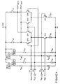
- Fig. 1 shows a known Gilbert cell used for realizing integrated IF parts such as variable gain amplifiers and mixers.
- a Gilbert cell two input voltages are multiplied into one output voltage, i.e. the voltage difference at the outputs is the product of the differences in the input voltages.
- a first voltage difference is coupled to terminals V X+ and V X- wherefrom the voltages are taken to the bases of transistors Q3, Q4 and Q6, Q7, respectively.
- a second voltage difference is coupled to terminals V Y+ and V Y- wherefrom the voltage is amplified by transistors Q5 and Q8.
- Transistors Q5 and Q8 are coupled through resistors R E1 and R E2 to a field effect transistor (FET) Q9 which is controlled by a bias voltage V BIAS and coupled to a negative operating voltage.
- Transistors Q3 and Q7 amplify a positive voltage difference V X+ and V X- , and the amplified voltage difference is coupled to outputs voltage through resistors R L1 and R L2 .
- Transistors Q2 and Q4 amplify a negative voltage difference V X+ and V X- , and the amplified voltage difference is crosscoupled to outputs V OUT+ and V OUT- .
- Fig. 2 shows in the form of flow diagram a balance adjustment method for a mixer according to the invention.
- possible previous bias voltages 1 are removed.
- the balance error 2 of the mixer is determined by coupling a radio signal to the receiver inputs, thus causing a spurious signal in the mixer, which is then measured at the mixer outputs.
- a bias voltage 3 correcting the balance error is set, preferably by feeding an inversely proportional CTRL byte corresponding to the error to the adjustment block by means of a digital controller. If the error-correcting bias voltage cannot be determined on the basis of the measurement result, a trial bias voltage is set.
- CTRL byte means a binary number that sets the control for the CTRL lines.
- the binary lines of the CTRL byte control the switching transistors in the adjustment block, so that I BIAS is changed and the voltages between the terminals of the bias resistors change.
- the potential of the operating point of the mixer's transistor input is adjusted according to the point between the bias resistors.
- the adjustment block forms a variable voltage across the resistor in the series connection when the adjustment is carried out by means of current.
- the adjustment block may also be implemented using a variable voltage source.
- the operational input signals of the transistors are alternating voltages conducted by a capacitive component. When the bias voltage that corrects or at least changes the balance error has been generated, it is checked whether the error correction was successful, i.e. whether the mixer is in balance 4.
- step 2 If not, operation returns to step 2 to determine the remaining error and change the bias voltages on the basis of that determination. If the setting of the bias reduced the balance error, the bias is increased, but if the balance error became bigger the bias is taken back towards zero or, if zero is reached, the bias is set on the second line of the input pair. Thus, bias voltage remains advantageously only on one of the lines of the input pair in the balanced state.
- the data of the balancing controller are stored in memory and normal operation of the mixer is started 5.
- Fig. 3 shows in a circuit diagram an adjustment block for the bias voltage of a mixer according to the invention.
- a current from a reference current source I REF flows via a transistor Q REF from the operating voltage VDD to ground.
- Current I REF is mirrored to a bias current circuit on the right.
- Current I BIASB through transistor Q BIASB constitutes the invariable fundamental part of bias current I BIAS .
- Transistors Q1, Q2, ... QN and Q1S, Q2S, ... QNS make up N parallel series connections, and a sum current of I 1 , I 2 , ... IN through said series connections constitutes the variable part of bias current I BIAS .
- Transistors Q1, Q2, ... QN are mutually binarily weighted such that transistors Q1S, Q2S, ... QNS, which are controlled by control lines CTRL 1, 2, ... N and connected in series with said transistors, can raise current I BIAS by 2 N -1 levels, which means the current gets 2 N values.
- Binary weighting of the currents is achieved e.g. by connecting transistors in parallel in such a way that Q1 comprises one transistor, Q2 comprises two transistors, etc. With field effect transistors (FET), the currents may also be set by selecting the channel widths.
- FET field effect transistors
- the currents are weighted preferably according to the following series: 1, 2, 4, 8, etc., i.e. 2 N , where N ⁇ 0.
- current I 1 is I REF /200
- current I 2 is I REF /100
- IN is I REF /(200/2 N-1 ).
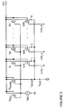
- Fig. 4 shows in a circuit diagram a mixer according to the invention.
- the blocks are for local oscillator signal pair V LO+ and V LO- and radio-frequency signal pair V RF+ and V RF- , which control through capacitive elements C1 and C2 as well as C3 and C4 the transistors Q10, Q11, Q13, Q14 and Q12, Q15.
- Blocks BLO+, BLO-, BRF+ and BRF- are used to produce currents and, thus, voltages to four parallel bias resistor series connections R B1 and R B2 , R B3 and R B4 , R B5 and R B6 as well as R B7 and R B8 .
- adjustment block current I BIAS is the same as the necessary base current of the corresponding transistor, e.g. a beta-compensated base current
- a resistor connected to ground is not used with that adjustment block. For example, if adjustment blocks BRF+ and BRF- feed the base current of transistors Q15 and Q12, resistors R B6 and R B8 are left out and the corresponding bias voltage is set by adjusting the base current.
- Load impedances Z L3 , Z L4 , transistors Q10, Q11, Q12,Q13, Q14, Q15 and emitter impedances Z E3 , Z E4 constitute a known mixer the outputs of which give signals V OUT+ and V OUT- .
- the balance is adjusted preferably as described above, but the most perfect balance is achieved by adjusting the bias voltages of the transistor pair's mutually corresponding transistors Q10, Q11 and Q13, Q14 separately.
- the controls of the transistors that get their control from the same line, such as Q10 and Q14, are separated from each other and the bias voltages of them both are adjusted individually.
- Fig. 5 shows in a circuit diagram a radio-frequency amplifier stage according to the invention which also can be used to correct a mixer's balance error.
- the blocks are for a radio-frequency signal pair V RF+ and V RF- which control through capacitive elements C5 and C6 transistors Q16 and Q17.
- Blocks BRF+ and BRF- are used to produce currents and, thus, voltages to two parallel bias resistor series connections R B9 , R B10 and R B11 , R B12 .
- Load impedances Z L5 , Z L6 , transistors Q16, Q17, emitter impedances Z E5 , Z E6 and current source I DIFF constitute a known radio-frequency amplifier stage.
- the circuit according to Fig. 5 described above can also be used as local oscillator buffer. Then the balance error of the local oscillator port can be corrected by adjusting the buffer.
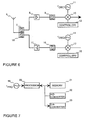
- Fig. 6 shows in the form of block diagram essential parts of a transceiver according to the invention.
- the transceiver shares a common antenna 6 from which a signal is received and filtered by a bandpass filter 7 and amplified by an amplifier 8 and refiltered 9. Then the signal at the radio reception frequency is mixed to an intermediate frequency in a balanced mixer 10 according to the invention.
- a local oscillator 11 feeds the mixer 10 at the frequency of f OSC1 .
- the balance of the mixer 10 is adjusted by a controller 12. From the intermediate frequency on the reception continues in accordance with the prior art.
- a signal to be transmitted is modulated at the local oscillator 14 frequency f OSC2 by means of a modulator 13.
- the balance of the modulator 13 is adjusted by a controller 15.
- the modulated signal is bandpass-filtered by a filter 16 and amplified by an amplifier 17 and filtered again by a filter 18 and fed to the antenna 6. Otherwise the transmitter is preferably realized according to the prior art, and this document does not take a position on the use of balancing according to the invention in it.
- Fig. 7 shows in a block diagram essential components of a controller of an adjustment block according to the invention.
- the processor 20 of a digital controller is stepped by an oscillator 19 at frequency F PRO .
- the controller executes a program from memory 21, which preferably is both read only memory (ROM) and random access memory (RAM). Measurement data on the balance is obtained by means of an A/D converter 22.
- Bias voltages are controlled by a D/A converter 23 which preferably comprises an adjustment block according to Fig. 3 in which current is switched by means of digital binary control to adjust the bias voltages.
- a radio receiver the spurious response of which is to be reduced.
- the receiver is adjusted preferably only once before use.
- a test signal is coupled to the receiver input, and the interfering signal level is measured from the receiver output.
- the test signal is generated in such a way that it produces a spurious response to be minimized.
- a trial setting is chosen e.g. for the adjustment block BRF+ of the positive line of the RF input, and the interfering signal level is measured again.
- Tuning data for the balance achieved through the minimization of spurious response are stored in the memory of the apparatus wherefrom they can be loaded by means of a microprocessor or digital signal processor (DSP) always on start-up. Fuses, microswitches, programmable gate circuits and the like can also be used for the immediate control of the adjustment block.
- DSP digital signal processor
- the selection of the bias voltage initial setting line and the level of the setting can also be realized as a preferably calculatory value based on interference measurement data.
- Empirical knowledge can also be utilized when estimating the bias voltage value on the basis of the measurement result.
- the received signal is converted digital.
- the method is advantageously applied in such a way that the spurious response is measured, adjusted as small as possible, and the settings are stored in memory by carrying out the necessary routines with a digital signal processor.
- the tuning is particularly fast as it is carried out by coupling a test signal to the antenna and executing a tuning program.
- the adjustment blocks are controlled by a microprocessor or preferably with the same digital signal processor.
- a serial or parallel bus is used for the control. For a serial bus an adjustment block needs a separate logic to control the transistors.
- the balance can also be tuned without a test signal while the local oscillator is operating.
- a comparative element is coupled to the mixer outputs to compare the voltage difference of the output pair. Particularly the DC component is compared. Tuning is performed by decreasing the voltage difference to its minimum value. However, because of bias voltages in the comparative element itself, the inputs of the comparative element must switch places and the comparison has to be repeated. The average of the tunings gives a result which is as accurate as possible. However, this tuning result is not as accurate as the one achieved using a test signal. If this type of tuning is accurate enough for the application, the tuning can be carried out automatically with a digital signal processor.
- the exemplary adjustment block was here realized by field effect transistors but the circuit can also be realized using bipolar transistors, for example.
Landscapes
- Engineering & Computer Science (AREA)
- Power Engineering (AREA)
- Superheterodyne Receivers (AREA)
- Noise Elimination (AREA)
Claims (13)
- Verfahren zum Vermindern von Störsignalen in einem Mischer eines Empfängers, bei welchem Funksignale von einer ersten Frequenz auf eine zweite Frequenz gemischt werden, wobei das Mischen in einer Gilbert-Zelle erfolgt, die vier obere Transistoren (Q10, Q11, Q13, Q14), welche ein Signal eines lokalen Oszillators an deren Basis empfangen, und zwei untere Transistoren (Q12, Q15), welche Signale einer ersten Frequenz an deren Basis empfangen und mit den vier oberen Transistoren (Q10, Q11, Q13, Q14) gekoppelt sind, aufweist, dadurch gekennzeichnet, daß der Mischer durch Einstellen von Bias-Spannungen (3) und/oder Strömen, die an der Basis von ausgewählten der oberen Transistoren anliegen, abgeglichen wird.
- Verfahren nach Anspruch 1, dadurch gekennzeichnet, daß Bias-Spannungen und/oder Ströme in einer Eingangsschaltung eingestellt werden (3), die eine Eingabe eines lokalen Oszillators (VLO+, VLO-) mit der Basis eines oberen Transistors (Q10, Q11, Q13, Q14) verbindet.
- Verfahren nach Anspruch 1 oder 2, dadurch gekennzeichnet, daß Bias-Spannungen und/oder Ströme in einer Eingangsschaltung eingestellt werden (3), welche die Signale einer ersten Frequenz empfängt und diese an die Basis eines unteren Transistors (Q12, Q15) koppelt.
- Verfahren nach Anspruch 1, 2 oder 3, dadurch gekennzeichnet, daß die Bias-Spannungen (3) und/oder Ströme unabhängig für beide Transistoren eines Transistorpaares einer Signalleitung in der Mischerschaltung eingestellt werden.
- Verfahren nach einem der vorstehenden Ansprüche 1 bis 4, dadurch gekennzeichnet, daß die Einstellung der Bias-Spannungen (3) und/oder Ströme mit Hilfe eines Digital-Analog-Wandlers durchgeführt wird, welcher einen Bias-Strom entsprechend eines geladenen Steuerungsbyte erzeugt.
- Verfahren nach einem der vorstehenden Ansprüche 1 bis 5, dadurch gekennzeichnet, daß die Bias-Spannungen (3) und/oder Ströme eingestellt werden, indem ein Abgleich an den Ausgängen des Empfängers, welcher den Mischer umfaßt, gemessen wird (2) und die Bias-Spannungen und/oder Ströme basierend auf den Messungen (4) empirisch eingestellt wird/werden (3).
- Empfänger mit einem Mischer (10) zum Mischen von Funksignalen von einer ersten Frequenz auf eine zweite Frequenz, umfassend:- eine Gilbert-Zelle mit vier oberen Transistoren (Q10, Q11, Q13, Q14), deren Basis mit Eingaben eines lokalen Oszillators des Mischers verbunden sind, und zwei unteren Transistoren (Q12, Q15), die angeschlossen sind, um die Signale einer ersten Frequenz an deren Basis zu empfangen, und die mit den vier oberen Transistoren (Q10, Q11, Q13, Q14) gekoppelt sind, und- ein Mittel zum Vermindern von Störsignalen,dadurch gekennzeichnet, daß
das Mittel zum Vermindern von Störsignalen ein Abgleicheinstellungsmittel (12) aufweist, welches konfiguriert ist, um den Mischerabgleich durch Einstellen von Bias-Spannungen und/oder Strömen einzustellen, die an der Basis von ausgewählten der oberen Transistoren (Q10, Q11, Q13, Q14) anliegen. - Empfänger nach Anspruch 7, dadurch gekennzeichnet, daß das Einstellungsmittel (12) einen Block (BLO+, BLO-), aufweist, der ausgebildet ist, um die Bias-Spannung einer Kopplung zwischen einer Eingabe eines lokalen Oszillators (VLO+, VLO-) und der Basis der oberen Transistoren, die mit dieser Eingabe eines lokalen Oszillators gekoppelt sind, zu steuern.
- Empfänger nach Anspruch 7 oder 8, dadurch gekennzeichnet, daß das Einstellungsmittel (12) einen Block (BRS+, BRS-) aufweist, welcher ausgebildet ist, um die Bias-Spannung von einer Kopplung zwischen einer Eingabe (VRF+, VRF-), welche die Signale einer ersten Frequenz empfängt, und der Basis des unteren Transistors, der mit dieser Eingabe gekoppelt ist, zu steuern.
- Empfänger nach Anspruch 7, 8 oder 9, dadurch gekennzeichnet, daß das Einstellungsmittel (12) sowohl einen Block (BLO+, BLO-) aufweist, der ausgebildet, um die Bias-Spannung einer Kopplung zwischen einer Eingabe eines lokalen Oszillators (VLO+, VLO-) und der Basis der unteren Transistoren, welche mit dieser Eingabe eines lokalen Oszillators gekoppelt sind, zu steuern, als auch einen Block (BRF+, BRF-) aufweist, der ausgebildet ist, um die Bias-Spannung einer Kopplung zwischen einer Eingabe (VRF+, VRF-), welche die Signale einer ersten Frequenz empfängt, und der Basis des unteren Transistors, welcher mit diesem Signal gekoppelt ist, zu steuern.
- Empfänger nach einem der vorstehenden Ansprüche 7 bis 10, dadurch gekennzeichnet, daß das Einstellungsmittel einen Digital-Analog-Wandler (19) aufweist, um die Bias-Spannungen und/oder Ströme mit einem digitalen Controller (12) zu steuern.
- Empfänger nach einem der vorstehenden Ansprüche 7 bis 11, dadurch gekennzeichnet, daß er weiter aufweist:- einen A/D-Wandler (18) zum Messen des Abgleiches,- einen D/A-Wandler (19) zum Einstellen von Bias-Spannungen und/oder Strömen, und- einen Oszillator (15), einen Prozessor (16) und einen Speicher (17), um Abgleich-Meßroutinen und Routinen zur Einstellung von einer Bias-Spannung und/oder eines Stromes auszuführen.
- Mobiles Gerät mit einem Empfänger nach einem der Ansprüche 7 bis 11.
Priority Applications (2)
| Application Number | Priority Date | Filing Date | Title |
|---|---|---|---|
| EP06027107A EP1764913A3 (de) | 1998-04-17 | 1999-04-16 | Empfänger zur Herabsetzung von Störsignalen |
| EP07008103.9A EP1811649B1 (de) | 1998-04-17 | 1999-04-16 | Verfahren zum Abschwächen von Störsignalen sowie Empfangsgerät |
Applications Claiming Priority (2)
| Application Number | Priority Date | Filing Date | Title |
|---|---|---|---|
| FI980858 | 1998-04-17 | ||
| FI980858A FI119214B (fi) | 1998-04-17 | 1998-04-17 | Menetelmä harhasignaalien vaimentamista varten ja vastaanotin |
Related Child Applications (2)
| Application Number | Title | Priority Date | Filing Date |
|---|---|---|---|
| EP07008103.9A Division EP1811649B1 (de) | 1998-04-17 | 1999-04-16 | Verfahren zum Abschwächen von Störsignalen sowie Empfangsgerät |
| EP06027107A Division EP1764913A3 (de) | 1998-04-17 | 1999-04-16 | Empfänger zur Herabsetzung von Störsignalen |
Publications (2)
| Publication Number | Publication Date |
|---|---|
| EP0951138A1 EP0951138A1 (de) | 1999-10-20 |
| EP0951138B1 true EP0951138B1 (de) | 2007-06-20 |
Family
ID=8551535
Family Applications (3)
| Application Number | Title | Priority Date | Filing Date |
|---|---|---|---|
| EP06027107A Withdrawn EP1764913A3 (de) | 1998-04-17 | 1999-04-16 | Empfänger zur Herabsetzung von Störsignalen |
| EP99660061A Expired - Lifetime EP0951138B1 (de) | 1998-04-17 | 1999-04-16 | Verfahren zur Herabsetzung von Störsignalen und Empfänger |
| EP07008103.9A Expired - Lifetime EP1811649B1 (de) | 1998-04-17 | 1999-04-16 | Verfahren zum Abschwächen von Störsignalen sowie Empfangsgerät |
Family Applications Before (1)
| Application Number | Title | Priority Date | Filing Date |
|---|---|---|---|
| EP06027107A Withdrawn EP1764913A3 (de) | 1998-04-17 | 1999-04-16 | Empfänger zur Herabsetzung von Störsignalen |
Family Applications After (1)
| Application Number | Title | Priority Date | Filing Date |
|---|---|---|---|
| EP07008103.9A Expired - Lifetime EP1811649B1 (de) | 1998-04-17 | 1999-04-16 | Verfahren zum Abschwächen von Störsignalen sowie Empfangsgerät |
Country Status (3)
| Country | Link |
|---|---|
| EP (3) | EP1764913A3 (de) |
| DE (1) | DE69936324T2 (de) |
| FI (1) | FI119214B (de) |
Families Citing this family (16)
| Publication number | Priority date | Publication date | Assignee | Title |
|---|---|---|---|---|
| US6871057B2 (en) * | 2000-03-08 | 2005-03-22 | Nippon Telegraph And Telephone Corporation | Mixer circuit |
| US6931083B1 (en) * | 2000-05-26 | 2005-08-16 | Telasic Communications, Inc. | Low noise, low distortion, muxable Gilbert mixer signal processing system and method with AGC functionality |
| FR2814607B1 (fr) * | 2000-09-26 | 2003-02-07 | St Microelectronics Sa | Polarisation d'un melangeur |
| US6785530B2 (en) * | 2001-03-16 | 2004-08-31 | Skyworks Solutions, Inc. | Even-order non-linearity correction feedback for Gilbert style mixers |
| WO2002084859A1 (en) | 2001-04-18 | 2002-10-24 | Nokia Corporation | Balanced circuit arrangement and method for linearizing such an arrangement |
| US6647273B2 (en) | 2001-12-28 | 2003-11-11 | Nokia Corporation | Method and apparatus for reducing power consumption in transceivers in wireless communications systems having a power control loop |
| FR2847744A1 (fr) * | 2002-11-26 | 2004-05-28 | St Microelectronics Sa | Procede de reduction de la non-linearite d'ordre deux d'un dispositif de transposition de frequence et dispositif correspondant |
| DE602005006585D1 (de) * | 2004-07-06 | 2008-06-19 | Acp Advanced Circuit Pursuit A | Symmetrischer mischer mit fets |
| US7356317B2 (en) * | 2004-07-14 | 2008-04-08 | Silicon Storage Technology, Inc. | Adaptive-biased mixer |
| DE102005028747B4 (de) | 2005-06-21 | 2010-12-16 | Infineon Technologies Ag | Mischeranordnung, Verwendung der Mischeranordnung und Verfahren zur Frequenzumsetzung |
| US8045944B2 (en) * | 2007-09-14 | 2011-10-25 | Qualcomm Incorporated | Offset correction for passive mixers |
| CN103999358B (zh) * | 2011-12-15 | 2017-09-01 | 马维尔国际贸易有限公司 | 具有对过程、温度和负载阻抗变化的不灵敏的rf功率检测电路 |
| GB2557637B (en) * | 2016-12-14 | 2022-06-22 | Bae Systems Plc | Variable frequency oscillator circuits and methods of generating an oscillating signal of a desired frequency |
| EP3349353A1 (de) * | 2017-01-12 | 2018-07-18 | BAE SYSTEMS plc | Oszillatorschaltungen mit veränderbarer frequenz und verfahren zur erzeugung eines oszillierenden signals gewünschter frequenz |
| US10931231B2 (en) | 2016-12-14 | 2021-02-23 | Bae Systems Plc | Variable frequency oscillator circuits and methods of generating an oscillating signal of a desired frequency |
| US12255586B2 (en) * | 2022-11-30 | 2025-03-18 | Qualcomm Incorporated | Oscillator feedthrough calibration |
Family Cites Families (7)
| Publication number | Priority date | Publication date | Assignee | Title |
|---|---|---|---|---|
| US5379457A (en) * | 1993-06-28 | 1995-01-03 | Hewlett-Packard Company | Low noise active mixer |
| US5392003A (en) * | 1993-08-09 | 1995-02-21 | Motorola, Inc. | Wide tuning range operational transconductance amplifiers |
| JP3565281B2 (ja) * | 1993-10-08 | 2004-09-15 | ソニー株式会社 | 受信機 |
| ZA95605B (en) * | 1994-04-28 | 1995-12-20 | Qualcomm Inc | Method and apparatus for automatic gain control and dc offset cancellation in quadrature receiver |
| JPH0856121A (ja) * | 1994-08-10 | 1996-02-27 | Advantest Corp | 周波数変換器 |
| US5613233A (en) * | 1994-09-30 | 1997-03-18 | Rockwell International Corp. | Apparatus with distortion cancelling feedback signal |
| US6138000A (en) * | 1995-08-21 | 2000-10-24 | Philips Electronics North America Corporation | Low voltage temperature and Vcc compensated RF mixer |
-
1998
- 1998-04-17 FI FI980858A patent/FI119214B/fi active IP Right Grant
-
1999
- 1999-04-16 DE DE69936324T patent/DE69936324T2/de not_active Expired - Lifetime
- 1999-04-16 EP EP06027107A patent/EP1764913A3/de not_active Withdrawn
- 1999-04-16 EP EP99660061A patent/EP0951138B1/de not_active Expired - Lifetime
- 1999-04-16 EP EP07008103.9A patent/EP1811649B1/de not_active Expired - Lifetime
Non-Patent Citations (1)
| Title |
|---|
| None * |
Also Published As
| Publication number | Publication date |
|---|---|
| FI980858L (fi) | 1999-10-18 |
| FI119214B (fi) | 2008-08-29 |
| EP1811649B1 (de) | 2013-09-18 |
| EP1811649A2 (de) | 2007-07-25 |
| EP0951138A1 (de) | 1999-10-20 |
| FI980858A0 (fi) | 1998-04-17 |
| EP1811649A3 (de) | 2007-08-08 |
| DE69936324D1 (de) | 2007-08-02 |
| EP1764913A3 (de) | 2007-04-04 |
| EP1764913A2 (de) | 2007-03-21 |
| DE69936324T2 (de) | 2008-02-21 |
Similar Documents
| Publication | Publication Date | Title |
|---|---|---|
| US6393260B1 (en) | Method for attenuating spurious signals and receiver | |
| EP0951138B1 (de) | Verfahren zur Herabsetzung von Störsignalen und Empfänger | |
| US7236761B2 (en) | Balanced circuit arrangement and method for linearizing such an arrangement | |
| RU2315423C2 (ru) | Калибровка подавления искажений | |
| US8411730B2 (en) | Semiconductor integrated communication circuit and operation method thereof | |
| AU641075B2 (en) | Apparatus and method of DC offset correction for a receiver | |
| US6366166B1 (en) | Double pass band amplifier circuit and a radio frequency reception head | |
| EP1501189B1 (de) | Hochfrequenzverstärker mit variabler Verstärkung, Regelvorrichtung, Hochfrequenzumsetzer mit variabler Verstärkung und Kommunikationsvorrichtung | |
| EP1414163A1 (de) | Empfänger und kommunikationsendgerät | |
| KR100794983B1 (ko) | 캐리어 누설을 억제하는 방법 및 시스템 | |
| US11581852B2 (en) | Systems and methods for detecting local oscillator leakage and image tone in I/Q mixer based transceivers | |
| US6088581A (en) | Method and apparatus for reducing amplitude modulated interference in a receiver | |
| US6771945B1 (en) | Dynamic DC balancing of a direct conversion receiver and method | |
| EP1236285B1 (de) | Empfängerschaltung | |
| US7555272B2 (en) | Transmission arrangement for transmitting data continuously in the time domain | |
| US7340232B2 (en) | Receiving system and semiconductor integrated circuit device for processing wireless communication signal | |
| JP2005057745A (ja) | 高周波可変利得増幅装置、制御装置、高周波可変利得周波数変換装置、および通信機器 | |
| EP1652292B1 (de) | Offsetkorrektur für abwärtsumsetzungsmischer | |
| US7272187B2 (en) | Filter circuit and radio apparatus | |
| US12483451B2 (en) | Transceiver circuit and associated control method |
Legal Events
| Date | Code | Title | Description |
|---|---|---|---|
| PUAI | Public reference made under article 153(3) epc to a published international application that has entered the european phase |
Free format text: ORIGINAL CODE: 0009012 |
|
| AK | Designated contracting states |
Kind code of ref document: A1 Designated state(s): DE FR GB IT |
|
| AX | Request for extension of the european patent |
Free format text: AL;LT;LV;MK;RO;SI |
|
| AKX | Designation fees paid |
Free format text: AT BE CH CY LI |
|
| 17P | Request for examination filed |
Effective date: 20000412 |
|
| RBV | Designated contracting states (corrected) |
Designated state(s): DE FR GB IT |
|
| REG | Reference to a national code |
Ref country code: DE Ref legal event code: 8566 |
|
| RAP1 | Party data changed (applicant data changed or rights of an application transferred) |
Owner name: NOKIA CORPORATION |
|
| 17Q | First examination report despatched |
Effective date: 20040802 |
|
| GRAP | Despatch of communication of intention to grant a patent |
Free format text: ORIGINAL CODE: EPIDOSNIGR1 |
|
| GRAS | Grant fee paid |
Free format text: ORIGINAL CODE: EPIDOSNIGR3 |
|
| GRAA | (expected) grant |
Free format text: ORIGINAL CODE: 0009210 |
|
| AK | Designated contracting states |
Kind code of ref document: B1 Designated state(s): DE FR GB IT |
|
| REG | Reference to a national code |
Ref country code: GB Ref legal event code: FG4D |
|
| RBV | Designated contracting states (corrected) |
Designated state(s): DE FR IT |
|
| REF | Corresponds to: |
Ref document number: 69936324 Country of ref document: DE Date of ref document: 20070802 Kind code of ref document: P |
|
| ET | Fr: translation filed | ||
| PLBE | No opposition filed within time limit |
Free format text: ORIGINAL CODE: 0009261 |
|
| STAA | Information on the status of an ep patent application or granted ep patent |
Free format text: STATUS: NO OPPOSITION FILED WITHIN TIME LIMIT |
|
| 26N | No opposition filed |
Effective date: 20080325 |
|
| REG | Reference to a national code |
Ref country code: DE Ref legal event code: R082 Ref document number: 69936324 Country of ref document: DE Representative=s name: SAMSON & PARTNER, PATENTANWAELTE, DE |
|
| REG | Reference to a national code |
Ref country code: FR Ref legal event code: TP Owner name: NOKIA TECHNOLOGIES OY, FI Effective date: 20150318 |
|
| REG | Reference to a national code |
Ref country code: DE Ref legal event code: R082 Ref document number: 69936324 Country of ref document: DE Representative=s name: SAMSON & PARTNER PATENTANWAELTE MBB, DE Effective date: 20150312 Ref country code: DE Ref legal event code: R081 Ref document number: 69936324 Country of ref document: DE Owner name: NOKIA TECHNOLOGIES OY, FI Free format text: FORMER OWNER: NOKIA CORP., 02610 ESPOO, FI Effective date: 20150312 |
|
| REG | Reference to a national code |
Ref country code: FR Ref legal event code: PLFP Year of fee payment: 18 |
|
| REG | Reference to a national code |
Ref country code: FR Ref legal event code: PLFP Year of fee payment: 19 |
|
| REG | Reference to a national code |
Ref country code: FR Ref legal event code: PLFP Year of fee payment: 20 |
|
| PGFP | Annual fee paid to national office [announced via postgrant information from national office to epo] |
Ref country code: FR Payment date: 20180315 Year of fee payment: 20 |
|
| PGFP | Annual fee paid to national office [announced via postgrant information from national office to epo] |
Ref country code: DE Payment date: 20180404 Year of fee payment: 20 |
|
| PGFP | Annual fee paid to national office [announced via postgrant information from national office to epo] |
Ref country code: IT Payment date: 20180420 Year of fee payment: 20 |
|
| REG | Reference to a national code |
Ref country code: DE Ref legal event code: R071 Ref document number: 69936324 Country of ref document: DE |