EP0951578B1 - Systeme de decapage et de depot de revetements de precision - Google Patents
Systeme de decapage et de depot de revetements de precision Download PDFInfo
- Publication number
- EP0951578B1 EP0951578B1 EP97950913A EP97950913A EP0951578B1 EP 0951578 B1 EP0951578 B1 EP 0951578B1 EP 97950913 A EP97950913 A EP 97950913A EP 97950913 A EP97950913 A EP 97950913A EP 0951578 B1 EP0951578 B1 EP 0951578B1
- Authority
- EP
- European Patent Office
- Prior art keywords
- sample
- chamber
- ion gun
- holder
- etching
- Prior art date
- Legal status (The legal status is an assumption and is not a legal conclusion. Google has not performed a legal analysis and makes no representation as to the accuracy of the status listed.)
- Expired - Lifetime
Links
Images


Classifications
-
- C—CHEMISTRY; METALLURGY
- C23—COATING METALLIC MATERIAL; COATING MATERIAL WITH METALLIC MATERIAL; CHEMICAL SURFACE TREATMENT; DIFFUSION TREATMENT OF METALLIC MATERIAL; COATING BY VACUUM EVAPORATION, BY SPUTTERING, BY ION IMPLANTATION OR BY CHEMICAL VAPOUR DEPOSITION, IN GENERAL; INHIBITING CORROSION OF METALLIC MATERIAL OR INCRUSTATION IN GENERAL
- C23C—COATING METALLIC MATERIAL; COATING MATERIAL WITH METALLIC MATERIAL; SURFACE TREATMENT OF METALLIC MATERIAL BY DIFFUSION INTO THE SURFACE, BY CHEMICAL CONVERSION OR SUBSTITUTION; COATING BY VACUUM EVAPORATION, BY SPUTTERING, BY ION IMPLANTATION OR BY CHEMICAL VAPOUR DEPOSITION, IN GENERAL
- C23C14/00—Coating by vacuum evaporation, by sputtering or by ion implantation of the coating forming material
- C23C14/22—Coating by vacuum evaporation, by sputtering or by ion implantation of the coating forming material characterised by the process of coating
- C23C14/56—Apparatus specially adapted for continuous coating; Arrangements for maintaining the vacuum, e.g. vacuum locks
- C23C14/564—Means for minimising impurities in the coating chamber such as dust, moisture, residual gases
- C23C14/566—Means for minimising impurities in the coating chamber such as dust, moisture, residual gases using a load-lock chamber
-
- C—CHEMISTRY; METALLURGY
- C23—COATING METALLIC MATERIAL; COATING MATERIAL WITH METALLIC MATERIAL; CHEMICAL SURFACE TREATMENT; DIFFUSION TREATMENT OF METALLIC MATERIAL; COATING BY VACUUM EVAPORATION, BY SPUTTERING, BY ION IMPLANTATION OR BY CHEMICAL VAPOUR DEPOSITION, IN GENERAL; INHIBITING CORROSION OF METALLIC MATERIAL OR INCRUSTATION IN GENERAL
- C23C—COATING METALLIC MATERIAL; COATING MATERIAL WITH METALLIC MATERIAL; SURFACE TREATMENT OF METALLIC MATERIAL BY DIFFUSION INTO THE SURFACE, BY CHEMICAL CONVERSION OR SUBSTITUTION; COATING BY VACUUM EVAPORATION, BY SPUTTERING, BY ION IMPLANTATION OR BY CHEMICAL VAPOUR DEPOSITION, IN GENERAL
- C23C14/00—Coating by vacuum evaporation, by sputtering or by ion implantation of the coating forming material
- C23C14/02—Pretreatment of the material to be coated
- C23C14/021—Cleaning or etching treatments
- C23C14/022—Cleaning or etching treatments by means of bombardment with energetic particles or radiation
-
- C—CHEMISTRY; METALLURGY
- C23—COATING METALLIC MATERIAL; COATING MATERIAL WITH METALLIC MATERIAL; CHEMICAL SURFACE TREATMENT; DIFFUSION TREATMENT OF METALLIC MATERIAL; COATING BY VACUUM EVAPORATION, BY SPUTTERING, BY ION IMPLANTATION OR BY CHEMICAL VAPOUR DEPOSITION, IN GENERAL; INHIBITING CORROSION OF METALLIC MATERIAL OR INCRUSTATION IN GENERAL
- C23C—COATING METALLIC MATERIAL; COATING MATERIAL WITH METALLIC MATERIAL; SURFACE TREATMENT OF METALLIC MATERIAL BY DIFFUSION INTO THE SURFACE, BY CHEMICAL CONVERSION OR SUBSTITUTION; COATING BY VACUUM EVAPORATION, BY SPUTTERING, BY ION IMPLANTATION OR BY CHEMICAL VAPOUR DEPOSITION, IN GENERAL
- C23C14/00—Coating by vacuum evaporation, by sputtering or by ion implantation of the coating forming material
- C23C14/22—Coating by vacuum evaporation, by sputtering or by ion implantation of the coating forming material characterised by the process of coating
- C23C14/34—Sputtering
- C23C14/46—Sputtering by ion beam produced by an external ion source
-
- G—PHYSICS
- G01—MEASURING; TESTING
- G01N—INVESTIGATING OR ANALYSING MATERIALS BY DETERMINING THEIR CHEMICAL OR PHYSICAL PROPERTIES
- G01N1/00—Sampling; Preparing specimens for investigation
- G01N1/28—Preparing specimens for investigation including physical details of (bio-)chemical methods covered elsewhere, e.g. G01N33/50, C12Q
- G01N1/32—Polishing; Etching
-
- H—ELECTRICITY
- H01—ELECTRIC ELEMENTS
- H01J—ELECTRIC DISCHARGE TUBES OR DISCHARGE LAMPS
- H01J37/00—Discharge tubes with provision for introducing objects or material to be exposed to the discharge, e.g. for the purpose of examination or processing thereof
- H01J37/30—Electron-beam or ion-beam tubes for localised treatment of objects
- H01J37/305—Electron-beam or ion-beam tubes for localised treatment of objects for casting, melting, evaporating, or etching
- H01J37/3053—Electron-beam or ion-beam tubes for localised treatment of objects for casting, melting, evaporating, or etching for evaporating or etching
-
- H—ELECTRICITY
- H01—ELECTRIC ELEMENTS
- H01J—ELECTRIC DISCHARGE TUBES OR DISCHARGE LAMPS
- H01J37/00—Discharge tubes with provision for introducing objects or material to be exposed to the discharge, e.g. for the purpose of examination or processing thereof
- H01J37/32—Gas-filled discharge tubes
- H01J37/34—Gas-filled discharge tubes operating with cathodic sputtering
Definitions
- the present invention relates to an apparatus for both etching and coating a specimen prior to analysis, and more particularly to an ion beam etching and sputter coating system for the preparation of sample specimens to be analyzed in a microscope.
- German Patent DD 224878 Al describes a process and apparatus comprising a vacuum chamber containing an ion gun for the vacuum etching of wafer substrates which are thereafter coated in the same chamber using the same ion gun and a movable target.
- the reference is unconcerned with the preparation or sample specimens to be analyzed in a microscope.
- Ion milling systems are used extensively for etching, milling, cutting, and cleaning samples of various materials such as ceramics, semiconductors, metals, and combinations thereof to make possible and/or enhance certain features for analysis in a microscope, typically analysis with an electron or optical microscope.
- Many of these samples, particularly samples of electrically insulating materials, are coated after cleaning or etching and prior to examination in an electron or optical microscope to prevent charging effects. Certain coatings also have the effect of increasing the secondary electron yield from almost all types of material.
- the samples to be studied are first mounted to a sample holder for the purpose of mechanically polishing one or more surfaces until such surfaces are flat, parallel, and scratch free.
- the polished sample is then removed from the polishing holder, mounted to a second holder, and placed into an ion milling device for etching.
- the sample is positioned in the path of one or more ion beams and etched at a relatively steep angle between the incident beam(s) and the sample surface.
- the sample may require remounting to a third holder to enable installation into a separate device for the purpose of depositing a conductive coating thereon.
- coatings were applied by such techniques as thermal evaporation, arc discharge, and diode, magnetron, or RF sputtering. More recently, the coatings have been applied by sputter coating in a vacuum using ion beam techniques.
- the sample may be mounted to a final stub or holder designed for use in a specific microscope, for example a transmission electron microscope, a scanning electron microscope, or even a light microscope.
- a specific microscope for example a transmission electron microscope, a scanning electron microscope, or even a light microscope.
- an apparatus for the precision etching and coating of a sample to be analyzed in a microscope includes a chamber communicating with a source of vacuum for forming and maintaining a vacuum in the chamber, The apparatus also includes a first ion gun positioned in the chamber and a sputtering target in the chamber.
- the apparatus is characterized in that it further comprises a sample holder onto which a sample is mounted and an airlock in the chamber for moving samples quickly into and out of the chamber.
- the first ion gun is adapted to etch the sample mounted on the sample holder, and at lease one additional ion gun is positioned in the chamber to cause material from the target to be directed onto the sample to coat the sample.
- the first ion gun is an ion milling gun which is positioned in the chamber to direct a stream of ions, neutrals, or combinations thereof onto the sample to etch the sample.
- the sputtering target is movable into a position for coating purposes.
- the target is shielded from the ion and neutrals stream emanating from the ion milling gun during etching.
- the at least one additional ion gun is positioned to direct a stream of ions and neutrals onto the target. After etching of the sample, the target is moved into a position in the chamber where material sputtered from it becomes coated onto the sample.
- the moveable target may be positioned to aid in efficiently directing sputtered material onto the sample.
- a process for the etching and sputter coating of a sample for analysis in a microscope including the steps of mounting the sample onto a sample holder and then loading the sample and holder into the evacuated chamber.
- the sample is etched in a vacuum using an ion milling gun which exposes the sample to a stream of energized ions and neutrals.
- the sample may be immediately coated in the same chamber without any need for further handling or transfer using a target material and an additional sputtering ion gun or guns which are provided in the chamber.
- the sample, still mounted in the sample holder is removed from the chamber and taken to a microscope for analysis.
- the target is moved into position, and the ion gun or guns are energized and produce energetic ions and neutrals which impinge onto the target and cause target material to be sputter deposited onto the sample.
- the coated sample may then be removed from the chamber. With the airlock, there is no need to continually cycle the pressure in the chamber from atmospheric to vacuum and back. Rather, the vacuum need be formed only once and then maintained.
- the sample By performing the etching and coating operations in the same chamber, the sample is not moved or handled between process steps, which minimizes the amount of contaminants to which the sample may be exposed. Further, the sample may be initially mounted onto a sample holder and then supported by that same holder throughout the entire etching/coating process. The same holder may even be used to support the sample for microscopic analysis.
- the sample is initially mounted onto a holder and then mechanically polished.
- the polished sample is then transferred into the vacuum chamber through an airlock where it is etched and then coaced.
- the finished, coated sample is then removed from the vacuum chamber ready for viewing in a selected microscope.
- the system and process of the present invention has some utility in sample preparation for scanning electron microscope (SEM) analysis, transmission electron microscope (TEM) analysis, and light microscope observations analysis. Accordingly, it is a feature of the present invention to provide for the etching and coating of samples in a single device under vacuum, thus minimizing handling and transfer of the samples.
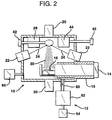
- the etching and coating system of the present invention includes a sealed chamber 10 which is evacuated by vacuum system 12 to provide a working pressure in the chamber.
- a sample holder 14 is used to mount a sample 16 therebn.
- Sample holder 14 may be cooled, such as by for example using liquid nitrogen, to reduce or maintain the temperature of sample 16 within a predetermined range as taught by Jones et al, U.S. Patent No. 4,950,901.
- Airlock 18 in a preferred embodiment, is pneumatically controlled to provide fast loading and unloading (i.e., 30 seconds) of the sample.
- fast loading and unloading i.e., 30 seconds
- the vacuum chamber 10 is only vented for routine servicing, allowing the base vacuum pressure to be maintained.
- a pneumatically-controlled airlock is described in Swann, U.S. Patent No. 4,272,682.
- Airlock 18 may vary in size and shape and may be designed to accept various configured sample holders as in the case of etching or coating TEM samples while mounted in a TEM holder or when a probe is used for monitoring the rate of sputtered coating deposition and total coating thickness.
- TEM sample holders vary in size and configuration according to manufacturer.
- a removable assembly may be provided into which sample holders of various preselected sizes and configurations may be inserted.
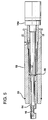
- Such a removable assembly comprises a reducing sleeve 52 and interchangeable adaptors 54 (only one shown), as illustrated in Fig. 5, which enable the accommodation of TEM sample holders of all varieties.
- reducing sleeve 52 has a generally cylindrical configuration and the same outer dimensions as a conventional sample holder 14 which it replaces.
- Sleeve 52 also has an inner diameter sized and adapted to fit the fixed outer diameter of an interchangeable adaptor 54.
- Interchangeable adaptors 54 have an inner diameter sized and adapted to accept TEM sample holders of various sizes and configurations such as sample holder 14a illustrated in Fig. 5.
- O-ring 55 provides a vacuum tight seal between adaptor 54 and the inner wall of pneumatic airlock piston 36 (also shown in Figs. 3 and 4).
- O-ring 57 provides a vacuum tight seal between adaptor 54 and sleeve 52.
- Sample holder 14a is fitted into adaptor 54 with a vacuum tight seal being provided by O-ring 57 in sample holder 14a.
- the portion of the TEM sample holder 14a which contains the sample 16 itself is extended into sealed chamber 10 by the operation of airlock 18.
- sample 16 is exposed to the ion beam for etching or to the sputtered target material 28 for coating.
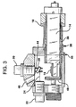
- sample 16 is secured to a sample mount 32, and mount 32 is inserted into a sample adaptor 34. The entire assembly is then inserted into sample holder 14.
- sample holder 14 is housed in airlock 18 and is moved into and out of position by a pneumatic piston 36. Gas pressure is provided to the piston from a source of compressed gas (not shown) connected through port 38. Airlock vacuum is achieved by connection 40 which communicates with a vacuum pump (not shown).
- Sample holder 14 may be designed to either "rock or rotate” or “rock and rotate” during the etching, cleaning, and/or coating processes. Such rocking and/or rotating mechanisms are known in this art. Rotation of the sample during etching produces a more uniformly etched sample surface and a more uniform etching rate. Rocking and rotating the sample during coating produces homogeneous coatings of uniform thickness.
- a fixed rock angle may be selected to change the incident angle of the ion beam on the sample surface from an angle normal to the sample surface to that of a lesser angle. The fixed angle also helps to increase the size of the etched area when combined with rotation.
- an ion etch gun 20 is positioned in chamber 10 as shown to provide the relative beam angle between the incident beam 21 and the sample surface.
- Gun 20 may be mounted at the top of chamber 10 as shown, or at the bottom, or at a location which would provide angled etching of the sample.
- gun 20 may be positioned so as to vary the distance between the gun and the surface of the sample. That is, gun 20 may be moved inwardly or outwardly from its position on the chamber wall. Moving gun 20 closer to the sample surface has the effect of increasing the etch rate for a given gun energy (keV). Such increased etch rate is useful where the gun is used for slope cutting of a sample or TEM sample milling.
- keV gun energy
- gun 20 may be mounted such that it is able to pivot. This provides the ability to change the angle at which the energetic ions and neutrals impinge the sample surface for a fixed, horizontally oriented sample. Thus, the angle of ion impingement could be adjusted without moving the sample.
- ion gun 20 may comprise a grounded cathode and an anode connected to an adjustable high voltage supply (not shown).
- a gas or combination of gases typically any noble or inert gas such as argon or xenon, may be supplied to the gun from a separate source 66.
- the high voltage discharge between the anode and cathode generates and directs an energetic beam 21 of ions and neutrals towards sample 16.
- Ion etch gun 20 may also comprise a rare earth magnet Penning gun which is capable of delivering a high current density ion beam which produces a high sample etching rate, reducing etching time.
- a second ion gun 20 may be positioned on the opposite side of chamber 10 as shown. Such a second gun would be able to provide simultaneous two-sided milling of samples for transmission electron microscopy (TEM).
- the ion gun or guns 20 may also be used to provide re-milling or cleanup of TEM samples which were initially prepared by broad ion beam (BIB) milling or focused ion beam (FIB) milling, or mechanically thinned using a known wedge technique.
- Such samples still mounted in a TEM holder, may be thinned using one or more ion guns to mill at shallow angles.
- the ion gun or guns 20 may also be used not only to clean (etch) stand-alone TEM samples but also samples mounted in a TEM sample holder, thus cleaning both the sample and holder simultaneously or cleaning the holder only. Such a cleaning improves high resolution imaging by removing amorphous layers and carbon-containing contaminants from the sample (and holder) surface by exposure to the etching beam at selected keV energies.
- target 28 is maintained in a shielded location (Figs. 1 and 4) out of the path of the ion beam.
- target 28 is carried on the tip of a retractable piston assembly 42 and can be moved from a retracted position (Fig. 1) out of the path of the ion gun to an extended position (Fig. 2).
- target shields 44 also shown in Fig. 3 and 4
- a vacuum system 12 which includes a drag pump manifold 60 which is in turn connected to molecular drag pump 62.
- Molecular drag pump 62 provides a suitable vacuum level for the operation of the ion guns by providing an ultimate vacuum of 10 -6 torr in sealed chamber 10.
- Molecular drag pump 62 will not operate properly unless its outlet is prepumped; therefore it is necessary to reduce its foreline or outlet vacuum. This is accomplished by backing molecular drag pump 62 with an oil free diaphragm pump 64.
- the oil free system is preferred to eliminate the possibility of introducing hydrocarbon contamination from the lubricating oils of the pump into sealed chamber 10.
- chamber 10 may include a viewing window 46.
- Window 46 provides an operator with a quick visual inspection of the working portion of vacuum chamber 10 to verify the correct operation of the device during rocking and/or rotation of the sample, the correct operation of the ion guns during etching or coating, and the correct positioning of shutter 48.
- the window also permits viewing of the sample to insure that it is properly positioned, has not slipped from its holder or mount, has not changed angle during movement of the holder or during loading or unloading through the airlock.
- ion etch gun 20 is turned off, and target 28 is moved into position.
- One or more ion sputter guns such as, for example, the pair of ion sputter guns 22 are activated and direct energetic beams of ions and neutrals at the target.
- Ion sputter guns may operate in the same general manner as ion etch gun 20.
- ion sputter guns 22 comprise rare earth magnet, Penning ion guns.
- Penning ion guns provide a high density ion flux and operate over a broad range of ion energies. Penning ion guns are advantageous as well in that they have low maintenance requirements, with no need for replacement of parts.
- the sputter deposits produced from the ion guns is high quality and amorphous.
- a sample such as a ceramic or semiconductor material
- a sample will be coated with a thin, amorphous layer of a conductive material.
- target 28 may comprise chromium, platinum, gold-palladium, iridium, tungsten, carbon, etc.
- Ion beams 24 from ion guns 22 cause target material 30 to be sputter deposited onto sample 16. The thickness of the deposited coating may be monitored using conventional techniques. Generally, the target may be sputter cleaned prior to deposition of the coating for a short initial period by exposing it to the energized stream of ions and neutrals.
- Figs. 3 and 4 there may be an independent rotatable shutter 48 so that the sample is protected during cleaning of the target.
- Fig. 3 illustrates the target in an extended working position such that the energized beam 24 contacts target 28 to sputter deposit material onto sample 16.
- rotatable shutter 48 is in an "open" position to expose the sample for coating.
- target 28 is shown in a retracted, shielded position as it would be during the etching procedure, and shutter 48 has been rotated to a "closed” position which can also be used to isolate the sample.
- Shutter 48 preferably comprises an electrically conductive material such as a metal which permits it to act as a Faraday cup or cage. By suitable connections (not shown), shutter 48 may also be used to monitor the ion current from first ion gun 20. Also, for purposes of understanding and illustration, the sample holder is shown in a retracted position within airlock chamber 50, and shutter 48 has been rotated to a "closed” position.
- the ion guns are turned off, and the sample is removed from chamber 10 through airlock 18.
- the sample may be loaded into or taken directly to a desired microscope for analysis.
- the apparatus and process of the present invention provide a technique which reduces sample handling and transfer to a minimum number of steps and substantially reduces the possibility of sample damage.
- the precision etching and coating system of the present invention may be used for ion beam slope cutting of samples. This is accomplished by using ion gun 20 and fixing the angle of a screened-mount sample holder to cross cut sections through heterogeneous solids such as, for example, integrated circuits and various semiconductor electronic devices.
- the screen which is mounted onto the sample holder comprises, for example, a block of metal having one or more sharply-defined knife edges.
- the metal of the screen serves as a protective mask for portions of the sample, while exposed areas of the sample are etched away. This provides the ability to investigate the cross-sectional microstructure of a device to reveal regions deep inside of the material for SEM observations and microanalysis. Once sufficiently etched, the sample is immediately sputter coated in chamber 10 with a desired target material using ion guns 22.
- the system of the present invention may also be used to wire shadow a TEM sample by cross sectioning the sample without glue line preparation. Again, once sufficiently etched, the sample is immediately sputter coated in chamber 10. While both beam slope cutting and wire shadowing are known techniques, the present system permits the etched and cut samples to be immediately sputter coated in the same vacuum chamber without needing to move the samples.
- the precision etching and coating system may also be used with chemical etching processes using non-inert gases such as reactive ion beam etching (RIBE) and chemically-assisted ion beam etching (CAIBE).
- non-inert gases such as reactive ion beam etching (RIBE) and chemically-assisted ion beam etching (CAIBE).
- RIBE reactive ion beam etching
- CAIBE chemically-assisted ion beam etching
- non-inert gases, and combinations thereof may be supplied to chamber 10 through an external source such as source 66 (as shown in Fig.2).
- Halogens and halogen-containing gases as well as oxidants such as oxygen and oxygen-containing gases and combinations of such gases including I 2 , Cl 2 , Br 2 , N 2 O 4 , CF 4 /O 2 , etc. produce superior results for special materials used in he semiconductor industry.
- the sample may be immediately sputter coated using the target material and
- the system of the present invention may also be used to sputter coat metallographic samples for micro-hardness tests and light microscope applications.
Landscapes
- Chemical & Material Sciences (AREA)
- Engineering & Computer Science (AREA)
- Metallurgy (AREA)
- Chemical Kinetics & Catalysis (AREA)
- Analytical Chemistry (AREA)
- Organic Chemistry (AREA)
- Physics & Mathematics (AREA)
- Mechanical Engineering (AREA)
- Materials Engineering (AREA)
- Plasma & Fusion (AREA)
- Health & Medical Sciences (AREA)
- Life Sciences & Earth Sciences (AREA)
- Pathology (AREA)
- Immunology (AREA)
- General Physics & Mathematics (AREA)
- General Health & Medical Sciences (AREA)
- Biochemistry (AREA)
- Sampling And Sample Adjustment (AREA)
- ing And Chemical Polishing (AREA)
- Physical Vapour Deposition (AREA)
Claims (37)
- Dispositif pour la gravure et le revêtement de précision d'un échantillon à analyser dans un microscope, comportant : une chambre (10) communiquant avec une source de vide (12) pour former et maintenir un vide dans ladite chambre, un premier canon à ions (20) positionné dans ladite chambre, et une cible de pulvérisation cathodique (28) dans ladite chambre, caractérisé en ce que le dispositif comporte de plus un support d'échantillon (14) sur lequel est monté un échantillon (16), un sas à air (18) dans ladite chambre à travers lequel ledit support d'échantillon est chargé et retiré, ledit premier canon à ions est adapté pour graver l'échantillon monté sur ledit support d'échantillon, et au moins un canon à ions supplémentaire (22) est positionné dans ladite chambre pour amener le matériau depuis ladite cible à être dirigé sur l'échantillon pour revêtir ledit échantillon.
- Dispositif selon la revendication 1, dans lequel ledit support d'échantillon est refroidi pour réduire ou maintenir la température dudit échantillon dans une plage prédéterminée.
- Dispositif selon la revendication 1, comportant une fenêtre de visualisation (46) dans ladite chambre.
- Dispositif selon la revendication 1, dans lequel ledit premier canon à ions peut être ajusté pour faire varier la distance entre ledit canon à ions et la surface dudit échantillon.
- Dispositif selon la revendication 1, dans lequel ledit premier canon à ions peut être mis en rotation pour altérer l'angle d'impact d'un flux d'ions et d'éléments neutres sur la surface dudit échantillon.
- Dispositif selon la revendication 1, comportant une protection (44) pour ladite cible de pulvérisation cathodique.
- Dispositif selon la revendication 6, dans lequel ladite cible de pulvérisation cathodique est mobile depuis une première position protégée jusqu'à une seconde position dans le trajet d'un flux d'ions et d'éléments neutres provenant dudit au moins un canon à ions supplémentaire.
- Dispositif selon la revendication 7, dans lequel ladite cible de pulvérisation cathodique est montée sur un ensemble de piston rétractable (42).
- Dispositif selon la revendication 1, comportant un obturateur (48) dans ladite chambre mobile depuis une première position protégeant ledit échantillon jusqu'à une seconde position hors du trajet d'un flux d'ions et d'éléments neutres provenant dudit premier canon à ions.
- Dispositif selon la revendication 9, dans lequel ledit obturateur comporte un matériau électrique conducteur qui agit en tant que coupe de Faraday.
- Dispositif selon la revendication 10, dans lequel le courant ionique provenant dudit premier canon à ions est contrôlé par ledit obturateur.
- Dispositif selon la revendication 1, dans lequel ladite source de vide comporte un système de mise sous vide sans huile comportant une pompe moléculaire (62) en combinaison avec une pompe à diaphragme (64).
- Dispositif selon la revendication 1, comportant de plus un ensemble amovible (52, 54) qui, en association avec ledit sas à air, permet l'insertion et le retrait des supports d'échantillon de dimensions et configurations présélectionnées.
- Dispositif selon la revendication 13, dans lequel ledit ensemble amovible comporte un manchon de réduction généralement cylindrique (52) et un adaptateur interchangeable généralement cylindrique (54), ledit manchon de réduction ayant un diamètre intérieur dimensionné et adapté pour s'ajuster au diamètre extérieur dudit adaptateur.
- Dispositif selon la revendication 14, dans lequel ledit adaptateur a un diamètre intérieur qui est dimensionné et adapté pour s'ajuster auxdits supports d'échantillon.
- Dispositif selon la revendication 1, dans lequel ledit support d'échantillon comporte dessus un bâti blindé.
- Procédé pour graver et revêtir un échantillon pour une analyse dans un microscope, comportant les étapes consistant à monter l'échantillon (16) sur un support d'échantillon (14), charger l'échantillon et le support dans une chambre de vide (10), graver l'échantillon dans un vide par exposition dudit échantillon à un flux d'ions et d'éléments neutres excités provenant d'un premier canon à ions (20) positionné dans ladite chambre, et revêtir l'échantillon gravé dans la même chambre par pulvérisation cathodique d'un matériau depuis une cible (28) dans ladite chambre sur ledit échantillon, caractérisé en ce que ladite étape de revêtement utilise au moins un canon à ions supplémentaire (22) positionné dans ladite chambre qui fait frapper un flux d'ions et d'éléments neutres excités sur ladite cible, et caractérisé de plus en ce que ledit échantillon revêtu est retiré de ladite chambre en étant monté sur ledit support d'échantillon.
- Procédé selon la revendication 17, dans lequel ledit échantillon et ledit support d'échantillon sont chargés dans ladite chambre à travers un sas à air (18) tout en maintenant ladite chambre dans une condition sous vide.
- Procédé selon la revendication 17, comportant l'étape consistant à polir mécaniquement la surface dudit échantillon avant de le charger dans ladite chambre.
- Procédé selon la revendication 17, comportant l'étape consistant à faire basculer et/ou tourner ledit échantillon lorsque ledit échantillon est gravé.
- Procédé selon la revendication 17, comportant l'étape consistant à faire basculer et/ou tourner ledit échantillon lorsque ledit échantillon est revêtu.
- Procédé selon la revendication 17, comportant l'étape consistant à nettoyer la surface de ladite cible en exposant un flux d'ions et d'éléments neutres excités tout en protégeant l'échantillon vis-à-vis dudit flux.
- Procédé selon la revendication 17, dans lequel ledit premier canon à ions peut être ajusté pour réduire la distance entre ledit canon et ledit échantillon afin d'augmenter la vitesse à laquelle ledit échantillon est gravé.
- Procédé selon la revendication 17, dans lequel ledit premier canon à ions peut être mis en rotation pour altérer l'angle d'impact desdits ions et éléments neutres excités.
- Procédé selon la revendication 17, comportant un canon à ions supplémentaire (22) positionné sur le côté opposé dudit échantillon par rapport audit premier canon à ions pour graver simultanément les deux surfaces dudit échantillon.
- Procédé selon la revendication 17, dans lequel ladite étape de gravure comporte l'introduction d'un ou de plusieurs gaz non-inertes dans ladite chambre.
- Procédé selon la revendication 17, comportant l'étape consistant à refroidir ledit support d'échantillon pour maintenir la température dudit échantillon dans une plage prédéterminée.
- Procédé selon la revendication 17, comportant les étapes consistant à nettoyer ledit support d'échantillon avant de monter ledit échantillon sur ledit support d'échantillon et à faire basculer ledit support d'échantillon lorsque ledit support d'échantillon est nettoyé.
- Procédé selon la revendication 17, comportant les étapes consistant à faire basculer ledit support d'échantillon lorsque l'échantillon est gravé.
- Procédé selon la revendication 17, comportant l'étape consistant à faire basculer ledit support d'échantillon lorsque ledit échantillon est revêtu.
- Procédé selon la revendication 17, dans lequel ladite étape de gravure utilise un gaz de traitement comportant une combinaison de gaz.
- Procédé selon la revendication 31, dans lequel au moins un desdits gaz de traitement est un gaz noble.
- Procédé selon la revendication 31, dans lequel ledit gaz noble est de l'argon.
- Procédé selon la revendication 31, dans lequel au moins un desdits gaz de traitement est un gaz oxydant.
- Procédé selon la revendication 34, dans lequel ledit gaz oxydant est de l'oxygène ou un gaz contenant de l'oxygène.
- Procédé selon la revendication 31, dans lequel au moins un desdits gaz de traitement est un gaz contenant de l'halogène.
- Procédé selon la revendication 31, dans lequel ledit gaz de traitement comporte I2, Cl2, Br2, N2O4, CF4/O2, et des mélanges de ceux-ci.
Applications Claiming Priority (3)
| Application Number | Priority Date | Filing Date | Title |
|---|---|---|---|
| US3349596P | 1996-12-20 | 1996-12-20 | |
| US33495P | 1996-12-20 | ||
| PCT/US1997/022640 WO1998028459A1 (fr) | 1996-12-20 | 1997-12-10 | Systeme de decapage et de depot de revetements de precision |
Publications (2)
| Publication Number | Publication Date |
|---|---|
| EP0951578A1 EP0951578A1 (fr) | 1999-10-27 |
| EP0951578B1 true EP0951578B1 (fr) | 2001-08-22 |
Family
ID=21870726
Family Applications (1)
| Application Number | Title | Priority Date | Filing Date |
|---|---|---|---|
| EP97950913A Expired - Lifetime EP0951578B1 (fr) | 1996-12-20 | 1997-12-10 | Systeme de decapage et de depot de revetements de precision |
Country Status (5)
| Country | Link |
|---|---|
| US (1) | US5922179A (fr) |
| EP (1) | EP0951578B1 (fr) |
| JP (1) | JP2001507165A (fr) |
| DE (1) | DE69706323T2 (fr) |
| WO (1) | WO1998028459A1 (fr) |
Families Citing this family (45)
| Publication number | Priority date | Publication date | Assignee | Title |
|---|---|---|---|---|
| JP2000035390A (ja) * | 1998-07-16 | 2000-02-02 | Seiko Instruments Inc | 薄片化加工方法 |
| US6388262B1 (en) | 1998-08-12 | 2002-05-14 | Gatan, Inc. | Double tilt and rotate specimen holder for a transmission electron microscope |
| JP2002542396A (ja) * | 1999-04-16 | 2002-12-10 | ユナキス・バルツェルス・アクチェンゲゼルシャフト | 加工物を真空処理する方法と真空処理装置 |
| AU2001263285A1 (en) | 2000-05-19 | 2001-12-03 | Imago Scientific Instruments | Methods of sampling specimens for microanalysis |
| US6768110B2 (en) * | 2000-06-21 | 2004-07-27 | Gatan, Inc. | Ion beam milling system and method for electron microscopy specimen preparation |
| WO2002031493A1 (fr) * | 2000-10-12 | 2002-04-18 | Kawasaki Steel Corporation | Procede pour traiter un echantillon d"analyse d"un metal et dispositif pour la mise en oeuvre dudit procede |
| US6458634B1 (en) | 2001-04-18 | 2002-10-01 | International Business Machines Corporation | Reduction of induced charge in SOI devices during focused ion beam processing |
| US20050118533A1 (en) * | 2002-03-01 | 2005-06-02 | Mirkarimi Paul B. | Planarization of substrate pits and scratches |
| US6891170B1 (en) | 2002-06-17 | 2005-05-10 | Zyvex Corporation | Modular manipulation system for manipulating a sample under study with a microscope |
| US6967335B1 (en) | 2002-06-17 | 2005-11-22 | Zyvex Corporation | Manipulation system for manipulating a sample under study with a microscope |
| EP1585999A4 (fr) * | 2002-08-02 | 2008-09-17 | E A Fischione Instr Inc | Procedes et appareil permettant de preparer des echantillons pour un examen microscopique |
| NL1021376C1 (nl) * | 2002-09-02 | 2004-03-03 | Fei Co | Werkwijze voor het verkrijgen van een deeltjes-optische afbeelding van een sample in een deeltjes-optisch toestel. |
| JP4297736B2 (ja) * | 2003-06-11 | 2009-07-15 | 株式会社日立ハイテクノロジーズ | 集束イオンビーム装置 |
| US6946064B2 (en) * | 2003-07-08 | 2005-09-20 | International Business Machines Corporation | Sample mount for performing sputter-deposition in a focused ion beam (FIB) tool |
| WO2005031789A2 (fr) * | 2003-09-23 | 2005-04-07 | Zyvex Corporation | Procede, systeme et dispositif pour examen microscopique faisant appel a un element de prehension destine a capturer un echantillon prepare par fib |
| TW200531420A (en) | 2004-02-20 | 2005-09-16 | Zyvex Corp | Positioning device for microscopic motion |
| US7285778B2 (en) * | 2004-02-23 | 2007-10-23 | Zyvex Corporation | Probe current imaging |
| US7326293B2 (en) * | 2004-03-26 | 2008-02-05 | Zyvex Labs, Llc | Patterned atomic layer epitaxy |
| KR101355280B1 (ko) * | 2004-08-24 | 2014-01-27 | 셀라 세미컨덕터 엔지니어링 라보라토리스 리미티드 | 워크피스를 밀링하기 위해 이온빔을 지향시키고 다수회 편향시키고, 그 정도를 결정 및 제어하기 위한 방법, 장치 및 시스템 |
| US7119333B2 (en) * | 2004-11-10 | 2006-10-10 | International Business Machines Corporation | Ion detector for ion beam applications |
| US7285775B2 (en) * | 2004-12-02 | 2007-10-23 | International Business Machines Corporation | Endpoint detection for the patterning of layered materials |
| US7256399B2 (en) * | 2005-04-07 | 2007-08-14 | International Business Machines Corporation | Non-destructive in-situ elemental profiling |
| EA008187B1 (ru) * | 2005-06-07 | 2007-04-27 | Владимир Яковлевич ШИРИПОВ | Способ очистки теневых масок в производстве дисплеев (варианты) и устройство для его реализации |
| JP2007225363A (ja) * | 2006-02-22 | 2007-09-06 | Hitachi Ltd | 磁気試料検査装置 |
| US7700917B1 (en) | 2007-10-04 | 2010-04-20 | Gatan, Inc. | Specimen holder with integral ion beam screen and in situ adjustment |
| JP5872541B2 (ja) | 2010-04-09 | 2016-03-01 | イー エイ フィシオネ インストルメンツ インコーポレーテッドE.A.Fischione Instruments, Inc. | 改良型イオン源 |
| US8384050B2 (en) | 2010-04-11 | 2013-02-26 | Gatan, Inc. | Ion beam sample preparation thermal management apparatus and methods |
| US8283642B2 (en) | 2010-04-11 | 2012-10-09 | Gatan, Inc. | Ion beam sample preparation apparatus and methods |
| US8445874B2 (en) * | 2010-04-11 | 2013-05-21 | Gatan Inc. | Ion beam sample preparation apparatus and methods |
| US8653489B2 (en) | 2010-04-11 | 2014-02-18 | Gatan, Inc. | Ion beam sample preparation apparatus and methods |
| WO2012060416A1 (fr) * | 2010-11-05 | 2012-05-10 | 株式会社 日立ハイテクノロジーズ | Dispositif de gravure ionique |
| FR2973811A1 (fr) * | 2011-04-08 | 2012-10-12 | Valeo Systemes Dessuyage | Installation pour le traitement par bombardement ionique de deux surfaces opposees |
| US8791438B2 (en) | 2012-07-27 | 2014-07-29 | Gatan Inc. | Ion beam sample preparation apparatus and methods |
| US10110854B2 (en) | 2012-07-27 | 2018-10-23 | Gatan, Inc. | Ion beam sample preparation apparatus and methods |
| US20150137003A1 (en) * | 2013-11-21 | 2015-05-21 | United Microelectronics Corp. | Specimen preparation method |
| US10731246B2 (en) * | 2014-07-28 | 2020-08-04 | Gatan, Inc. | Ion beam sample preparation and coating apparatus and methods |
| JP6258826B2 (ja) * | 2014-09-19 | 2018-01-10 | 日本電子株式会社 | 試料作製装置 |
| JP6515320B2 (ja) * | 2014-11-19 | 2019-05-22 | 日本製鉄株式会社 | 試料ホルダー及び透過型電子顕微鏡による観察方法 |
| JP6811860B2 (ja) * | 2017-06-21 | 2021-01-13 | 株式会社日立ハイテク | 荷電粒子線装置およびクリーニング方法 |
| GB2587940B (en) * | 2018-04-02 | 2023-06-14 | Applied Materials Inc | Inline chamber metrology |
| JP7097777B2 (ja) * | 2018-08-10 | 2022-07-08 | 東京エレクトロン株式会社 | 成膜装置および成膜方法 |
| US11170973B2 (en) * | 2019-10-09 | 2021-11-09 | Applied Materials, Inc. | Temperature control for insertable target holder for solid dopant materials |
| JP7544819B2 (ja) | 2019-12-05 | 2024-09-03 | サイエンコンス アクスイェ セルスカプ | 高度に精製された212Pbの製造 |
| CN113281197B (zh) * | 2021-05-13 | 2022-11-15 | 中物院成都科学技术发展中心 | 一种可多维运动的垂直轻气炮 |
| US11854760B2 (en) | 2021-06-21 | 2023-12-26 | Applied Materials, Inc. | Crucible design for liquid metal in an ion source |
Family Cites Families (19)
| Publication number | Priority date | Publication date | Assignee | Title |
|---|---|---|---|---|
| CH625641A5 (en) * | 1977-05-13 | 1981-09-30 | Battelle Memorial Institute | Method for carrying out a deposition in a luminescent discharge on at least one substrate and an ion etching of this substrate |
| US4340815A (en) * | 1977-11-07 | 1982-07-20 | Ion Tech Limited | Preparation of material for examination by transmission electron microscopy techniques |
| US4272682A (en) * | 1979-08-10 | 1981-06-09 | Gatan, Inc. | Specimen elevator for an ion milling machine |
| DE3211022A1 (de) * | 1981-03-31 | 1982-11-11 | Ion Tech Ltd., Teddington, Middlesex | Verfahren und vorrichtung zur bereitstellung einer fuer die untersuchung mit einem elektronenmikroskop geeigneten probe |
| DD224878A1 (de) * | 1984-06-28 | 1985-07-17 | Hochvakuum Dresden Veb | Verfahren zur vollautomatischen handhabung von substratscheiben in einer ionenstrahlaetzanlage |
| US4793908A (en) * | 1986-12-29 | 1988-12-27 | Rockwell International Corporation | Multiple ion source method and apparatus for fabricating multilayer optical films |
| US4913789A (en) * | 1988-04-18 | 1990-04-03 | Aung David K | Sputter etching and coating process |
| US4923585A (en) * | 1988-11-02 | 1990-05-08 | Arch Development Corporation | Sputter deposition for multi-component thin films |
| US5178957A (en) * | 1989-05-02 | 1993-01-12 | Minnesota Mining And Manufacturing Company | Noble metal-polymer composites and flexible thin-film conductors prepared therefrom |
| US5091049A (en) * | 1989-06-13 | 1992-02-25 | Plasma & Materials Technologies, Inc. | High density plasma deposition and etching apparatus |
| US5009743A (en) * | 1989-11-06 | 1991-04-23 | Gatan Incorporated | Chemically-assisted ion beam milling system for the preparation of transmission electron microscope specimens |
| US4992398A (en) * | 1989-12-29 | 1991-02-12 | Motorola, Inc. | High frequency dielectric composition |
| US5292419A (en) * | 1990-12-20 | 1994-03-08 | Leybold Aktiengesellschaft | Sputtering unit |
| US5650378A (en) * | 1992-10-02 | 1997-07-22 | Fujikura Ltd. | Method of making polycrystalline thin film and superconducting oxide body |
| US5336550A (en) * | 1993-05-18 | 1994-08-09 | Applied Magnetics Corporation | Carbon overcoat for magnetic head sliders |
| US5393376A (en) * | 1993-12-30 | 1995-02-28 | International Business Machines Corporation | Method of making pole tip structure for thin film magnetic heads |
| US5472566A (en) * | 1994-11-14 | 1995-12-05 | Gatan, Inc. | Specimen holder and apparatus for two-sided ion milling system |
| US5628659A (en) * | 1995-04-24 | 1997-05-13 | Microelectronics And Computer Corporation | Method of making a field emission electron source with random micro-tip structures |
| US5633502A (en) * | 1995-08-11 | 1997-05-27 | E. A. Fischione Instruments, Inc. | Plasma processing system for transmission electron microscopy specimens and specimen holders |
-
1997
- 1997-10-20 US US08/954,080 patent/US5922179A/en not_active Expired - Lifetime
- 1997-12-10 DE DE69706323T patent/DE69706323T2/de not_active Expired - Lifetime
- 1997-12-10 WO PCT/US1997/022640 patent/WO1998028459A1/fr not_active Ceased
- 1997-12-10 JP JP52881198A patent/JP2001507165A/ja active Pending
- 1997-12-10 EP EP97950913A patent/EP0951578B1/fr not_active Expired - Lifetime
Also Published As
| Publication number | Publication date |
|---|---|
| US5922179A (en) | 1999-07-13 |
| WO1998028459A1 (fr) | 1998-07-02 |
| DE69706323T2 (de) | 2002-02-07 |
| JP2001507165A (ja) | 2001-05-29 |
| EP0951578A1 (fr) | 1999-10-27 |
| DE69706323D1 (de) | 2001-09-27 |
Similar Documents
| Publication | Publication Date | Title |
|---|---|---|
| EP0951578B1 (fr) | Systeme de decapage et de depot de revetements de precision | |
| US6914244B2 (en) | Ion beam milling system and method for electron microscopy specimen preparation | |
| EP1630849B1 (fr) | Traitement localisé par plasma | |
| US5986264A (en) | Ion beam preparation device for electron microscopy | |
| EP1998356B1 (fr) | Préparation d'échantillon STEM in situ | |
| JP5600371B2 (ja) | 荷電粒子ビーム処理のための保護層のスパッタリング・コーティング | |
| US5976328A (en) | Pattern forming method using charged particle beam process and charged particle beam processing system | |
| EP1803140B1 (fr) | Dispositif et procede pour broyer un materiau au moyen d'ions | |
| Mukhopadhyay | Sample preparation for microscopic and spectroscopic characterization of solid surfaces and films | |
| US9318306B2 (en) | Interchangeable sputter gun head | |
| JP7818615B2 (ja) | 均一なイオン切削に適するシステム及び方法 | |
| US20130168231A1 (en) | Method For Sputter Deposition And RF Plasma Sputter Etch Combinatorial Processing | |
| Alani et al. | A New ion Beam Based Etching/Coating System for Scanning Electron Microscopy (SEM) and Light Microscopy (LM) | |
| Cerchiara et al. | Recent developments in automated sample preparation for FESEM |
Legal Events
| Date | Code | Title | Description |
|---|---|---|---|
| PUAI | Public reference made under article 153(3) epc to a published international application that has entered the european phase |
Free format text: ORIGINAL CODE: 0009012 |
|
| 17P | Request for examination filed |
Effective date: 19990325 |
|
| AK | Designated contracting states |
Kind code of ref document: A1 Designated state(s): DE FR GB |
|
| 17Q | First examination report despatched |
Effective date: 19991201 |
|
| GRAG | Despatch of communication of intention to grant |
Free format text: ORIGINAL CODE: EPIDOS AGRA |
|
| GRAG | Despatch of communication of intention to grant |
Free format text: ORIGINAL CODE: EPIDOS AGRA |
|
| GRAH | Despatch of communication of intention to grant a patent |
Free format text: ORIGINAL CODE: EPIDOS IGRA |
|
| GRAH | Despatch of communication of intention to grant a patent |
Free format text: ORIGINAL CODE: EPIDOS IGRA |
|
| GRAA | (expected) grant |
Free format text: ORIGINAL CODE: 0009210 |
|
| AK | Designated contracting states |
Kind code of ref document: B1 Designated state(s): DE FR GB |
|
| REF | Corresponds to: |
Ref document number: 69706323 Country of ref document: DE Date of ref document: 20010927 |
|
| ET | Fr: translation filed | ||
| REG | Reference to a national code |
Ref country code: GB Ref legal event code: IF02 |
|
| PLBE | No opposition filed within time limit |
Free format text: ORIGINAL CODE: 0009261 |
|
| STAA | Information on the status of an ep patent application or granted ep patent |
Free format text: STATUS: NO OPPOSITION FILED WITHIN TIME LIMIT |
|
| 26N | No opposition filed | ||
| REG | Reference to a national code |
Ref country code: DE Ref legal event code: R082 Ref document number: 69706323 Country of ref document: DE Representative=s name: MEHLER ACHLER PATENTANWAELTE PARTNERSCHAFT MBB, DE Ref country code: DE Ref legal event code: R082 Ref document number: 69706323 Country of ref document: DE Representative=s name: MEHLER ACHLER PATENTANWAELTE, DE |
|
| REG | Reference to a national code |
Ref country code: FR Ref legal event code: PLFP Year of fee payment: 19 |
|
| REG | Reference to a national code |
Ref country code: FR Ref legal event code: PLFP Year of fee payment: 20 |
|
| PGFP | Annual fee paid to national office [announced via postgrant information from national office to epo] |
Ref country code: GB Payment date: 20161207 Year of fee payment: 20 Ref country code: DE Payment date: 20161206 Year of fee payment: 20 Ref country code: FR Payment date: 20161111 Year of fee payment: 20 |
|
| REG | Reference to a national code |
Ref country code: DE Ref legal event code: R071 Ref document number: 69706323 Country of ref document: DE |
|
| REG | Reference to a national code |
Ref country code: GB Ref legal event code: PE20 Expiry date: 20171209 |
|
| PG25 | Lapsed in a contracting state [announced via postgrant information from national office to epo] |
Ref country code: GB Free format text: LAPSE BECAUSE OF EXPIRATION OF PROTECTION Effective date: 20171209 |