EP0952508A1 - Circuit générateur de tension de référence - Google Patents
Circuit générateur de tension de référence Download PDFInfo
- Publication number
- EP0952508A1 EP0952508A1 EP99105491A EP99105491A EP0952508A1 EP 0952508 A1 EP0952508 A1 EP 0952508A1 EP 99105491 A EP99105491 A EP 99105491A EP 99105491 A EP99105491 A EP 99105491A EP 0952508 A1 EP0952508 A1 EP 0952508A1
- Authority
- EP
- European Patent Office
- Prior art keywords
- bipolar transistor
- voltage
- reference voltage
- emitter
- current
- Prior art date
- Legal status (The legal status is an assumption and is not a legal conclusion. Google has not performed a legal analysis and makes no representation as to the accuracy of the status listed.)
- Granted
Links
- 230000005540 biological transmission Effects 0.000 claims description 2
- 238000010586 diagram Methods 0.000 description 5
- 230000005669 field effect Effects 0.000 description 3
- 229910052710 silicon Inorganic materials 0.000 description 2
- 239000010703 silicon Substances 0.000 description 2
- 239000000758 substrate Substances 0.000 description 2
- 230000015572 biosynthetic process Effects 0.000 description 1
- 230000007423 decrease Effects 0.000 description 1
- 230000001419 dependent effect Effects 0.000 description 1
- 238000005516 engineering process Methods 0.000 description 1
- 230000013011 mating Effects 0.000 description 1
- 230000006641 stabilisation Effects 0.000 description 1
- 238000011105 stabilization Methods 0.000 description 1
Images


Classifications
-
- G—PHYSICS
- G05—CONTROLLING; REGULATING
- G05F—SYSTEMS FOR REGULATING ELECTRIC OR MAGNETIC VARIABLES
- G05F3/00—Non-retroactive systems for regulating electric variables by using an uncontrolled element, or an uncontrolled combination of elements, such element or such combination having self-regulating properties
- G05F3/02—Regulating voltage or current
- G05F3/08—Regulating voltage or current wherein the variable is DC
- G05F3/10—Regulating voltage or current wherein the variable is DC using uncontrolled devices with non-linear characteristics
- G05F3/16—Regulating voltage or current wherein the variable is DC using uncontrolled devices with non-linear characteristics being semiconductor devices
- G05F3/20—Regulating voltage or current wherein the variable is DC using uncontrolled devices with non-linear characteristics being semiconductor devices using diode- transistor combinations
- G05F3/22—Regulating voltage or current wherein the variable is DC using uncontrolled devices with non-linear characteristics being semiconductor devices using diode- transistor combinations wherein the transistors are of the bipolar type only
- G05F3/222—Regulating voltage or current wherein the variable is DC using uncontrolled devices with non-linear characteristics being semiconductor devices using diode- transistor combinations wherein the transistors are of the bipolar type only with compensation for device parameters, e.g. Early effect, gain, manufacturing process, or external variations, e.g. temperature, loading, supply voltage
- G05F3/225—Regulating voltage or current wherein the variable is DC using uncontrolled devices with non-linear characteristics being semiconductor devices using diode- transistor combinations wherein the transistors are of the bipolar type only with compensation for device parameters, e.g. Early effect, gain, manufacturing process, or external variations, e.g. temperature, loading, supply voltage producing a current or voltage as a predetermined function of the temperature
-
- G—PHYSICS
- G05—CONTROLLING; REGULATING
- G05F—SYSTEMS FOR REGULATING ELECTRIC OR MAGNETIC VARIABLES
- G05F3/00—Non-retroactive systems for regulating electric variables by using an uncontrolled element, or an uncontrolled combination of elements, such element or such combination having self-regulating properties
- G05F3/02—Regulating voltage or current
- G05F3/08—Regulating voltage or current wherein the variable is DC
- G05F3/10—Regulating voltage or current wherein the variable is DC using uncontrolled devices with non-linear characteristics
- G05F3/16—Regulating voltage or current wherein the variable is DC using uncontrolled devices with non-linear characteristics being semiconductor devices
- G05F3/20—Regulating voltage or current wherein the variable is DC using uncontrolled devices with non-linear characteristics being semiconductor devices using diode- transistor combinations
- G05F3/26—Current mirrors
- G05F3/265—Current mirrors using bipolar transistors only
-
- G—PHYSICS
- G05—CONTROLLING; REGULATING
- G05F—SYSTEMS FOR REGULATING ELECTRIC OR MAGNETIC VARIABLES
- G05F3/00—Non-retroactive systems for regulating electric variables by using an uncontrolled element, or an uncontrolled combination of elements, such element or such combination having self-regulating properties
- G05F3/02—Regulating voltage or current
- G05F3/08—Regulating voltage or current wherein the variable is DC
- G05F3/10—Regulating voltage or current wherein the variable is DC using uncontrolled devices with non-linear characteristics
- G05F3/16—Regulating voltage or current wherein the variable is DC using uncontrolled devices with non-linear characteristics being semiconductor devices
- G05F3/20—Regulating voltage or current wherein the variable is DC using uncontrolled devices with non-linear characteristics being semiconductor devices using diode- transistor combinations
- G05F3/26—Current mirrors
- G05F3/267—Current mirrors using both bipolar and field-effect technology
Definitions
- the present invention relates to a reference voltage generating circuit or reference voltage source according to the preamble of claim 1.
- Known reference voltage sources use, for example, Zener diodes, to which an unstabilized input voltage is supplied via a series resistor, the voltage tapped at the Zener diode being used as the voltage-stabilized reference voltage.
- the forward or forward voltage of a diode or the base-emitter voltage of a bipolar transistor can in principle be used as a reference voltage.
- the forward voltage of a pn junction has a negative temperature coefficient and thus a temperature dependency that is negative for many applications. If, for example, sensors, A / D converters or similar components are to be supplied with the aid of a voltage regulator, the output voltage of which serves as a reference voltage, the output voltage of the voltage regulator must be highly precise and, in particular, extremely temperature-stable.
- tolerance limits of up to 1% are normal requirements.
- bandgap or Bandgap reference voltage sources have been replaced by bandgap or Bandgap reference voltage sources replaced, which provide a temperature-stabilized reference voltage.
- bandgap reference voltage sources are based on an addition of a forward voltage of a current-carrying pn junction and a differential voltage multiplied by a corresponding factor, which is formed from two forward voltages of two pn junctions through which different current densities flow.
- the forward voltage of a current-carrying pn junction - as has already been explained above - has a negative temperature coefficient.
- the difference between two forward voltages increases proportionally to the absolute temperature and is therefore subject to a positive temperature coefficient.
- the factor by which the differential voltage explained above is multiplied is set such that the negative temperature coefficient of the forward voltage of the pn junction cancels the positive temperature coefficient of the differential voltage, a temperature-stabilized output or reference voltage can be obtained which only has a parabolic or exhibits quadratic temperature dependence.
- the output voltage of the bandgap reference voltage source which is obtained by adding the previously explained forward voltage of a current-carrying pn junction with the difference voltage multiplied by the corresponding factor of two further forward voltages, is approximately 1.25 V, which is approximately the band gap (band gap ) of silicon.
- the magnitude of the output voltage of this reference voltage source has therefore given the bandgap reference voltage source its name.
- a current mirror circuit S 1 which connects the collector currents I 1 and I 2 from two npn bipolar transistors T 1 and T 2 connected according to FIG. 2, is connected to a positive supply voltage connection V cc compares.
- the currents of these currents I 1 and I 2 are predetermined by the transistors T 1 and T 2 .
- the base terminals of these transistors T 1 and T 2 are connected to each other, wherein the base voltage of the transistor T is multiplied up 1 via a voltage divider consisting of two resistors R 5 and R 6, so that the resistor R 6 ref a desired initial or reference voltage V can be tapped.
- the current mirror S 1 has an output which reproduces the result of the comparison of the currents I 1 and I 2 and is coupled to an actuator ST, for example an operational amplifier or an amplifying transistor.
- the emitter current densities of transistors T 1 and T 2 differ by the factor n ⁇ m, ie the emitter current density of transistor T 1 is (n ⁇ m) times as large as the emitter current density of the transistor T 2 .
- the total voltage is tapped from the base-emitter voltage of the transistor T 1 and the voltage present at the node between the resistors R 1 and R 2 .
- the first-mentioned base-emitter voltage of the transistor T 1 corresponds to the forward voltage of a current-carrying pn junction and therefore, as has been explained above, has a negative temperature coefficient.
- the voltage drop across the resistor R 1 is dependent on the difference between the base-emitter voltage of the transistor T 1 and the base-emitter voltage of the transistor T 2 and, as has also been explained above, has a positive temperature coefficient.
- the emitter-base voltage of the bipolar transistor T 1 decreases by 2mV / K depending on the temperature.
- the bandgap reference voltage source shown in FIG. 2 can be dimensioned in such a way that the differential voltage across the resistor R 1 from the forward voltages of the two transistors T 1 and T 2 is one by appropriate selection of the resistors R 1 and R 2 and the previously specified factor n the negative temperature coefficient compensating positive temperature coefficient of + 2mV / K is subject.
- the invention is therefore based on the object of specifying a reference voltage generating circuit of the type described at the outset, which is less sensitive to temperature fluctuations and component tolerances.
- the reference voltage is further generated by adding a voltage component with a negative temperature coefficient to a voltage component with a positive temperature coefficient.
- the portion subject to the negative temperature coefficient comprises a plurality of forward voltages of corresponding pn junctions
- the portion with the positive temperature coefficient in turn comprises a differential voltage, each voltage contributing to the differential voltage corresponding to a sum voltage from a plurality of forward voltages of corresponding pn junctions.
- the difference voltage which represents the proportion of the desired reference voltage with a positive temperature coefficient, is the difference between two sums of several forward voltages with different current densities through pn junctions.
- the reference voltage source provides an output voltage that is a multiple of the usual bandgap reference voltage. This voltage is sufficiently high for most applications, so that, for example, a voltage divider for high multiplication of the reference voltage can be omitted.
- the reference voltage source according to the invention By appropriate dimensioning of the reference voltage source according to the invention it can be achieved that a deviation of 1K in the temperature of one of the transistors used is only 1.3% of the difference in the total voltages. Furthermore, it is possible to arrange the transistors in the layout of the reference voltage source according to the invention in such a way that linear temperature gradients cannot falsify the output voltage of the reference voltage source from any direction.
- circuit means are used which compensate for the remaining parabolic temperature dependency of the generated reference voltage, so that the output reference voltage can ideally be generated in a temperature-stable manner within a 0.03% window.
- the previously described principle known per se is used in turn to add the reference voltage by adding a component with a negative temperature coefficient and a component with a positive temperature coefficient generate, whereby by suitable circuit dimensioning the negative temperature coefficient can be compensated for by the positive temperature coefficient.
- the portion of the generated reference voltage which is subject to a positive temperature coefficient is the difference between two summation voltages from a plurality of forward voltages of pn junctions through which different current densities flow.
- the portion that is subject to the negative temperature coefficient comprises the sum of the forward voltages of several pn junctions.
- the circuit shown in FIG. 1 again comprises npn transistors T 1 and T 2 , the emitter areas A E1 and A E2 of which are in the ratio 1: n 1 .
- the transistors T 1 and T 2 are operated with collector currents I 1 and I 2 , respectively, which are compared by a current mirror circuit S 1 , the current strengths of these currents I 1 and I 2 being predetermined by the transistors T 1 and T 2 .
- the base connections of the transistors T 1 and T 2 are separately connected to the emitters of further npn bipolar transistors T 3 and T 4 .
- the emitter areas A E3 and A E4 of the transistors T 3 and T 4 are in a ratio of 1: n 2 .
- the transistors T 3 and T 4 are flowed through by different currents I 3 and I 4 , which can be set via resistors R 3 and R 4 .
- the collectors of the transistors T 3 and T 4 are connected to a positive supply voltage potential V CC .
- the base connections of the transistors T 3 and T 4 are connected to one another.
- the resistors R 1 and R 2 are connected to the transistors T 1 and T 2 in accordance with the known reference voltage source shown in FIG. 2.
- a diode D or a corresponding pn junction is coupled to the resistor R 3 .
- the voltage across resistor R 4 corresponds to the difference between the emitter-base voltages of transistors T 3 and T 4 . So that the ratio of the emitter currents of these transistors is temperature stable, the voltage across resistor R 3 must also be proportional to temperature. This is achieved with the aid of the diode D, since the voltage at R 1 increases in proportion to the temperature and the forward voltages of the bipolar transistor T 1 and the diode D do not differ significantly, so that the voltage across the resistor R 3, as desired, is proportional to the temperature.
- the desired reference or output voltage is tapped at the common base connection of the bipolar transistors T 3 and T 4 .
- This output voltage corresponds to the total voltage from the base-emitter voltages of the transistors T 3 and T 1 and the voltage present at the node between the resistors R 1 and R 2 .
- the base-emitter voltages of the transistors T 3 and T 1 are known to have a negative temperature coefficient of approximately -2 mV / K.
- the voltage present at the node between the resistors R 1 and R 2 is determined by the base-emitter voltages of the transistors T 1 -T 4 and corresponds in particular to the difference between a first voltage and the sum of the forward voltages of those through which a high current density flows Transistors T 1 and T 3 depends, and a second voltage, which depends on the sum of the forward voltages of the bipolar transistors T 2 and T 4 through which a low current density flows. That is, the voltage present at the node between the resistors R 1 and R 2 depends on the difference between the sum of the base-emitter voltages of the transistors T 1 and T 3 and the sum of the base-emitter voltages of the transistors T 2 and T 4 from.
- the differential voltage present at the node between the resistors R 1 and R 2 has such a positive temperature coefficient which the negative temperature coefficient of the base-emitter voltages the bipolar transistors T 3 and T 1 compensated.
- the positive temperature coefficient of the differential voltage drop across the resistor R 1 must be as high as the negative temperature coefficient of the base-emitter voltages of the transistors T 3 and T 1 and consequently be approximately + 4mV / K.
- the voltage of approximately 2.5 V present at the common base of the transistors T 3 and T 4 is sufficiently high for most applications, so that in principle the use of a voltage divider with resistors R 5 and R 6 for high multiplication of the reference voltage can be omitted . Therefore, in the circuit shown in FIG. 1, the voltage divider with the resistors R 5 and R 6 is only shown in broken lines.
- the circuit shown in Fig. 1 can be modified in a simple manner such that not only the difference is formed from two summation voltages, but that the difference is formed from several summation voltages by using a correspondingly larger number of bipolar transistors, each of these summation voltages corresponds to an addition of even three or more forward voltages of pn junctions through which different current densities flow.
- the circuit shown in FIG. 1 can be modified in such a way that a voltage which corresponds to a multiple of the bandgap of silicon is generally tapped at the base terminal of the transistor T 3 .
- the emitter current of the bipolar transistor T 4 can be chosen to be very small, since the greatest thermal leakage current from the collector of each npn transistor to the substrate in barrier-layer-insulated bipolar technologies does not enter the emitter current of the in the present case corresponding npn transistor is received.
- a deviation of the temperature of one of the bipolar transistors T 1 - T 4 by 1K is only 1.3% in this differential voltage, so that the reference voltage circuit shown in Fig. 1 is less sensitive to temperature fluctuations or temperature gradients.
- the resistance ratio R 1 : R 2 can be set to 4: 1 by a clever choice of the individual components shown in FIG. 1. This is a ratio that can be adjusted particularly precisely.
- an actuator ST is again coupled to the output terminal of the current mirror S 1 in the circuit shown in FIG. 1, which is controlled as a function of the comparison result of the current mirror S1 in order to avoid an uneven load on the latter Output connection to allow readjustment of the output voltage V ref .
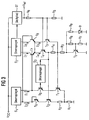
- FIG. 1 shows a refined exemplary embodiment of the reference voltage source according to the invention, the corresponding components being provided with the same reference numerals and a repeated description of these components being dispensed with.
- a further current mirror circuit S 2 which compares collector currents I 7 and I 8 from further transistors T 7 and T 8 and controls the actuator ST depending on the comparison result.
- These bipolar transistors T 3 and T 4 form an amplifier stage in order to keep the current consumption of the reference voltage source shown in FIG. 3 as low as possible.
- current mirror S 1 With current mirror S 1 , the inputs correspond to the outputs and are connected to the base connections of transistors T 7 and T 8 .
- Another npn bipolar transistor T 5 together with another current mirror circuit S 3, serves to compensate for the errors arising from the base current of transistor T 2 .
- the bipolar transistor T 5 has an emitter area corresponding to the emitter area of the bipolar transistor T 2
- the bipolar transistor T 6 has an emitter area corresponding to the emitter area of the bipolar transistor T 1 , ie the emitter area of the bipolar transistor T 5 is n 1 times as large as the emitter area of the bipolar transistor M 6 .
- a circuit arrangement is coupled to the resistor R 3 , which, in addition to the diode D already shown in FIG. 1 in accordance with FIG. 3, has connected resistors R 7 -R 9 and a further bipolar transistor T 9 .
- This circuit arrangement works as follows. At low temperatures, the current flow through the resistor R 3 is smallest and the flow voltages of all pn junctions are so high that the resistors R7 and R8 essentially determine the behavior of this circuit arrangement.
- the path leading via the diode D and the resistor R 9 dominates , in which case the resistance of the equivalent circuit diagram of this circuit arrangement is lower due to the parallel connection of R 8 and R 7 to R 9 and the diode voltage by the factor (R 8 + R 7 ) / (R 7 + R 8 + R 9 ) is divided down.
- the path leading through transistor T 9 dominates, the equivalent circuit diagram having a diode forward voltage increased by the factor (R 7 + R 8 ) / R 7 without series resistance.
- FIG. 4 shows an example of a double band gap reference voltage source implemented on a test chip according to the present invention. Again, those components that correspond to the components shown in FIG. 3 are given the same reference numerals and will not be explained again.
- the current mirror S 1 shown in Figure 3 includes p-channel MOS field effect transistors M 3 - M 6 and n-channel MOS field effect transistors M 7 - M 10.
- the current mirror circuit S 2 is implemented by a pnp bipolar transistor T 11 .
- the reference potential of the current mirrors S 1 and S 3 corresponds to the input potential of the actuator ST, which is realized by an actuating transistor M 11 .
- the reference potential of the current mirror S 2 is connected to the reference potential of the control transistor M 11 .
- the previously described relationship of the reference potentials is not absolutely necessary.
- the resistor R 10 additionally shown in FIG. 4 serves to compensate for the thermal leakage current of the resistor R 4 .
- the components T 12 , T 13 , C 1 - C 3 and R 11 serve to stabilize the circuit.
- the diode D shown in FIG. 3 is realized by the pn junction of a further bipolar transistor T 10 , the base-collector path of which is short-circuited. Otherwise, the mode of operation of the reference voltage source shown in FIG. 4 corresponds to that of the circuits shown in FIGS. 1 and 3.
Landscapes
- Engineering & Computer Science (AREA)
- Microelectronics & Electronic Packaging (AREA)
- Physics & Mathematics (AREA)
- Nonlinear Science (AREA)
- Electromagnetism (AREA)
- General Physics & Mathematics (AREA)
- Radar, Positioning & Navigation (AREA)
- Automation & Control Theory (AREA)
- Control Of Electrical Variables (AREA)
Applications Claiming Priority (2)
| Application Number | Priority Date | Filing Date | Title |
|---|---|---|---|
| DE19818464 | 1998-04-24 | ||
| DE19818464A DE19818464A1 (de) | 1998-04-24 | 1998-04-24 | Referenzspannung-Erzeugungsschaltung |
Publications (2)
| Publication Number | Publication Date |
|---|---|
| EP0952508A1 true EP0952508A1 (fr) | 1999-10-27 |
| EP0952508B1 EP0952508B1 (fr) | 2001-08-29 |
Family
ID=7865738
Family Applications (1)
| Application Number | Title | Priority Date | Filing Date |
|---|---|---|---|
| EP99105491A Expired - Lifetime EP0952508B1 (fr) | 1998-04-24 | 1999-03-17 | Circuit générateur de tension de référence |
Country Status (5)
| Country | Link |
|---|---|
| US (1) | US6046578A (fr) |
| EP (1) | EP0952508B1 (fr) |
| DE (2) | DE19818464A1 (fr) |
| ES (1) | ES2163909T3 (fr) |
| PT (1) | PT952508E (fr) |
Cited By (2)
| Publication number | Priority date | Publication date | Assignee | Title |
|---|---|---|---|---|
| CN101336400B (zh) * | 2005-12-02 | 2010-09-01 | 德州仪器公司 | 精确反向带隙电压参考电路及方法 |
| CN115951744A (zh) * | 2022-12-20 | 2023-04-11 | 小华半导体有限公司 | 基极电流产生电路 |
Families Citing this family (16)
| Publication number | Priority date | Publication date | Assignee | Title |
|---|---|---|---|---|
| US6292050B1 (en) | 1997-01-29 | 2001-09-18 | Cardiac Pacemakers, Inc. | Current and temperature compensated voltage reference having improved power supply rejection |
| US6154018A (en) * | 1999-09-01 | 2000-11-28 | Vlsi Technology, Inc. | High differential impedance load device |
| US6381491B1 (en) | 2000-08-18 | 2002-04-30 | Cardiac Pacemakers, Inc. | Digitally trimmable resistor for bandgap voltage reference |
| US6340882B1 (en) * | 2000-10-03 | 2002-01-22 | International Business Machines Corporation | Accurate current source with an adjustable temperature dependence circuit |
| US6380723B1 (en) * | 2001-03-23 | 2002-04-30 | National Semiconductor Corporation | Method and system for generating a low voltage reference |
| US6677808B1 (en) | 2002-08-16 | 2004-01-13 | National Semiconductor Corporation | CMOS adjustable bandgap reference with low power and low voltage performance |
| US7088085B2 (en) * | 2003-07-03 | 2006-08-08 | Analog-Devices, Inc. | CMOS bandgap current and voltage generator |
| US7834610B2 (en) * | 2007-06-01 | 2010-11-16 | Faraday Technology Corp. | Bandgap reference circuit |
| GB2452324A (en) * | 2007-09-03 | 2009-03-04 | Adaptalog Ltd | Temperature sensor or bandgap regulator |
| JP5072718B2 (ja) * | 2008-06-02 | 2012-11-14 | 株式会社東芝 | 信号受信装置 |
| US8981736B2 (en) * | 2010-11-01 | 2015-03-17 | Fairchild Semiconductor Corporation | High efficiency, thermally stable regulators and adjustable zener diodes |
| US9448579B2 (en) * | 2013-12-20 | 2016-09-20 | Analog Devices Global | Low drift voltage reference |
| EP3021189B1 (fr) * | 2014-11-14 | 2020-12-30 | ams AG | Source de tension de référence et un procédé permettant de générer une tension de référence |
| KR20160072703A (ko) * | 2014-12-15 | 2016-06-23 | 에스케이하이닉스 주식회사 | 기준전압 생성회로 |
| DE102021134256A1 (de) | 2021-12-22 | 2023-06-22 | Infineon Technologies Ag | Start-up-Schaltung |
| CN119045600B (zh) * | 2024-10-29 | 2025-01-07 | 东莞市通科电子有限公司 | 一种半导体集成电路及其温漂补偿方法 |
Citations (3)
| Publication number | Priority date | Publication date | Assignee | Title |
|---|---|---|---|---|
| DE3119048A1 (de) * | 1980-05-28 | 1982-03-25 | Ebauches Electroniques S.A., 2074 Marin, Neuchâtel | "spannungspegeldetektor" |
| WO1993009597A1 (fr) * | 1991-10-29 | 1993-05-13 | Lattice Semiconductor Corporation | Convertisseur de tension en courant de cmos a compensation de temperature |
| EP0676856A2 (fr) * | 1994-04-11 | 1995-10-11 | Rockwell International Corporation | Convertisseur continu-continu, efficient, bien réglé, élévateur de tension, pour circuits intégrés CMO |
Family Cites Families (6)
| Publication number | Priority date | Publication date | Assignee | Title |
|---|---|---|---|---|
| JPS5927326A (ja) * | 1982-08-02 | 1984-02-13 | Hitachi Ltd | 定電圧回路 |
| DE3682855D1 (de) * | 1985-09-17 | 1992-01-23 | Siemens Ag | Schaltungsanordnung zur erzeugung einer referenzspannung mit vorgebbarer temperaturdrift. |
| BE1007853A3 (nl) * | 1993-12-03 | 1995-11-07 | Philips Electronics Nv | Bandgapreferentiestroombron met compensatie voor spreiding in saturatiestroom van bipolaire transistors. |
| JP3347896B2 (ja) * | 1994-10-21 | 2002-11-20 | 日本オプネクスト株式会社 | 定電圧源回路 |
| FR2737319B1 (fr) * | 1995-07-25 | 1997-08-29 | Sgs Thomson Microelectronics | Generateur de reference de tension et/ou de courant en circuit integre |
| FR2750514A1 (fr) * | 1996-06-26 | 1998-01-02 | Philips Electronics Nv | Dispositif de regulation de tension a faible dissipation interne d'energie |
-
1998
- 1998-04-24 DE DE19818464A patent/DE19818464A1/de not_active Withdrawn
-
1999
- 1999-03-17 EP EP99105491A patent/EP0952508B1/fr not_active Expired - Lifetime
- 1999-03-17 PT PT99105491T patent/PT952508E/pt unknown
- 1999-03-17 ES ES99105491T patent/ES2163909T3/es not_active Expired - Lifetime
- 1999-03-17 DE DE59900215T patent/DE59900215D1/de not_active Expired - Lifetime
- 1999-04-26 US US09/299,363 patent/US6046578A/en not_active Expired - Lifetime
Patent Citations (3)
| Publication number | Priority date | Publication date | Assignee | Title |
|---|---|---|---|---|
| DE3119048A1 (de) * | 1980-05-28 | 1982-03-25 | Ebauches Electroniques S.A., 2074 Marin, Neuchâtel | "spannungspegeldetektor" |
| WO1993009597A1 (fr) * | 1991-10-29 | 1993-05-13 | Lattice Semiconductor Corporation | Convertisseur de tension en courant de cmos a compensation de temperature |
| EP0676856A2 (fr) * | 1994-04-11 | 1995-10-11 | Rockwell International Corporation | Convertisseur continu-continu, efficient, bien réglé, élévateur de tension, pour circuits intégrés CMO |
Cited By (2)
| Publication number | Priority date | Publication date | Assignee | Title |
|---|---|---|---|---|
| CN101336400B (zh) * | 2005-12-02 | 2010-09-01 | 德州仪器公司 | 精确反向带隙电压参考电路及方法 |
| CN115951744A (zh) * | 2022-12-20 | 2023-04-11 | 小华半导体有限公司 | 基极电流产生电路 |
Also Published As
| Publication number | Publication date |
|---|---|
| PT952508E (pt) | 2002-01-30 |
| EP0952508B1 (fr) | 2001-08-29 |
| DE19818464A1 (de) | 1999-10-28 |
| DE59900215D1 (de) | 2001-10-04 |
| US6046578A (en) | 2000-04-04 |
| ES2163909T3 (es) | 2002-02-01 |
Similar Documents
| Publication | Publication Date | Title |
|---|---|---|
| EP0952508B1 (fr) | Circuit générateur de tension de référence | |
| DE19530472B4 (de) | Konstantstromschaltung | |
| DE1813326C3 (de) | Integrierte Schaltung zum Vorspannen der Basis-Emitter-Strecke eines Transistors durch eine temperaturabhängige Vorspannung | |
| DE102011001346B4 (de) | Rauscharme Bandlückenreferenzen | |
| EP0421516B1 (fr) | Dispositif d'alimentation avec régulation de tension et limiteur de courant | |
| EP0160836B1 (fr) | Capteur de température | |
| DE2154904B2 (de) | Temperaturkompensierte Bezugsgleichspannungsquelle | |
| EP0080567B1 (fr) | Source de courant intégrée à semiconducteurs | |
| DE3836338A1 (de) | Temperaturkompensierte stromquellenschaltung mit zwei anschluessen | |
| DE2457753A1 (de) | Temperaturkompensierte elektronische spannungsquelle | |
| EP0508327A2 (fr) | Circuit de référence du type Bandgap | |
| DE2440795B2 (de) | Temperaturabhängiger Spannungsgeber | |
| DE3241364A1 (de) | Digital gesteuerte praezisionsstromquelle mit einem offenen kompensationskreis | |
| DE102017125831A1 (de) | Temperaturkompensierte Referenzspannungsschaltung | |
| DE2260405B2 (de) | Bezugsspannungsgeneratorschaltung | |
| DE102019124383A1 (de) | Proportional-zu-Absoluttemperatur-Schaltung, Verfahren, Spannungsreferenz und Spannungsreferenzschaltung | |
| DE2750998A1 (de) | Bezugsspannungsschaltung | |
| EP0216265B1 (fr) | Circuit pour générer une tension de référence comportant une dérive en température prévisible | |
| DE3230429C2 (fr) | ||
| DE2438255A1 (de) | Stromverstaerker | |
| EP0506174B1 (fr) | Dispositif à circuit intégré comprenant un amplificateur différentiel | |
| DE3788033T2 (de) | Spannungsregler mit Präzisionsthermostromquelle. | |
| EP0237086B1 (fr) | Circuit de miroir de courant | |
| DE3110355C2 (de) | Gleichspannungsgenerator zur Lieferung einer temperaturabhängigen Ausgangs-Gleichspannung | |
| EP0952509B1 (fr) | Circuit de tension de référence |
Legal Events
| Date | Code | Title | Description |
|---|---|---|---|
| PUAI | Public reference made under article 153(3) epc to a published international application that has entered the european phase |
Free format text: ORIGINAL CODE: 0009012 |
|
| AK | Designated contracting states |
Kind code of ref document: A1 Designated state(s): DE ES FR GB IE IT PT |
|
| AX | Request for extension of the european patent |
Free format text: AL;LT;LV;MK;RO;SI |
|
| 17P | Request for examination filed |
Effective date: 19991206 |
|
| AKX | Designation fees paid |
Free format text: DE ES FR GB IE IT PT |
|
| GRAG | Despatch of communication of intention to grant |
Free format text: ORIGINAL CODE: EPIDOS AGRA |
|
| 17Q | First examination report despatched |
Effective date: 20000912 |
|
| RAP1 | Party data changed (applicant data changed or rights of an application transferred) |
Owner name: INFINEON TECHNOLOGIES AG |
|
| GRAG | Despatch of communication of intention to grant |
Free format text: ORIGINAL CODE: EPIDOS AGRA |
|
| GRAH | Despatch of communication of intention to grant a patent |
Free format text: ORIGINAL CODE: EPIDOS IGRA |
|
| GRAH | Despatch of communication of intention to grant a patent |
Free format text: ORIGINAL CODE: EPIDOS IGRA |
|
| GRAA | (expected) grant |
Free format text: ORIGINAL CODE: 0009210 |
|
| AK | Designated contracting states |
Kind code of ref document: B1 Designated state(s): DE ES FR GB IE IT PT |
|
| REG | Reference to a national code |
Ref country code: IE Ref legal event code: FG4D Free format text: GERMAN |
|
| REF | Corresponds to: |
Ref document number: 59900215 Country of ref document: DE Date of ref document: 20011004 |
|
| GBT | Gb: translation of ep patent filed (gb section 77(6)(a)/1977) |
Effective date: 20011117 |
|
| REG | Reference to a national code |
Ref country code: GB Ref legal event code: IF02 |
|
| EN | Fr: translation not filed | ||
| REG | Reference to a national code |
Ref country code: PT Ref legal event code: SC4A Free format text: AVAILABILITY OF NATIONAL TRANSLATION Effective date: 20011031 |
|
| REG | Reference to a national code |
Ref country code: ES Ref legal event code: FG2A Ref document number: 2163909 Country of ref document: ES Kind code of ref document: T3 |
|
| PLBE | No opposition filed within time limit |
Free format text: ORIGINAL CODE: 0009261 |
|
| STAA | Information on the status of an ep patent application or granted ep patent |
Free format text: STATUS: NO OPPOSITION FILED WITHIN TIME LIMIT |
|
| 26N | No opposition filed | ||
| PGFP | Annual fee paid to national office [announced via postgrant information from national office to epo] |
Ref country code: GB Payment date: 20030226 Year of fee payment: 5 |
|
| PGFP | Annual fee paid to national office [announced via postgrant information from national office to epo] |
Ref country code: PT Payment date: 20040218 Year of fee payment: 6 Ref country code: IE Payment date: 20040218 Year of fee payment: 6 |
|
| PG25 | Lapsed in a contracting state [announced via postgrant information from national office to epo] |
Ref country code: GB Free format text: LAPSE BECAUSE OF NON-PAYMENT OF DUE FEES Effective date: 20040317 |
|
| PGFP | Annual fee paid to national office [announced via postgrant information from national office to epo] |
Ref country code: ES Payment date: 20040322 Year of fee payment: 6 |
|
| ET | Fr: translation filed | ||
| REG | Reference to a national code |
Ref country code: FR Ref legal event code: ERR Free format text: BOPI DE PUBLICATION N: 02/04 PAGES: 245 PARTIE DU BULLETIN CONCERNEE: BREVETS EUROPEENS DONT LA TRADUCTION N'A PAS ETE REMISE A I'INPI IL Y A LIEU DE SUPPRIMER: LA MENTION DE LA NON REMISE. LA REMISE DE LA TRADUCTION EST PUBLIEE DANS LE PRESENT BOPI. |
|
| GBPC | Gb: european patent ceased through non-payment of renewal fee |
Effective date: 20040317 |
|
| PG25 | Lapsed in a contracting state [announced via postgrant information from national office to epo] |
Ref country code: IE Free format text: LAPSE BECAUSE OF NON-PAYMENT OF DUE FEES Effective date: 20050317 |
|
| PG25 | Lapsed in a contracting state [announced via postgrant information from national office to epo] |
Ref country code: ES Free format text: LAPSE BECAUSE OF NON-PAYMENT OF DUE FEES Effective date: 20050318 |
|
| PG25 | Lapsed in a contracting state [announced via postgrant information from national office to epo] |
Ref country code: PT Free format text: LAPSE BECAUSE OF NON-PAYMENT OF DUE FEES Effective date: 20050919 |
|
| REG | Reference to a national code |
Ref country code: IE Ref legal event code: MM4A |
|
| REG | Reference to a national code |
Ref country code: ES Ref legal event code: FD2A Effective date: 20050318 |
|
| REG | Reference to a national code |
Ref country code: FR Ref legal event code: PLFP Year of fee payment: 18 |
|
| REG | Reference to a national code |
Ref country code: FR Ref legal event code: PLFP Year of fee payment: 19 |
|
| PGFP | Annual fee paid to national office [announced via postgrant information from national office to epo] |
Ref country code: FR Payment date: 20170322 Year of fee payment: 19 |
|
| PGFP | Annual fee paid to national office [announced via postgrant information from national office to epo] |
Ref country code: DE Payment date: 20170516 Year of fee payment: 19 |
|
| PGFP | Annual fee paid to national office [announced via postgrant information from national office to epo] |
Ref country code: IT Payment date: 20170323 Year of fee payment: 19 |
|
| REG | Reference to a national code |
Ref country code: DE Ref legal event code: R119 Ref document number: 59900215 Country of ref document: DE |
|
| PG25 | Lapsed in a contracting state [announced via postgrant information from national office to epo] |
Ref country code: DE Free format text: LAPSE BECAUSE OF NON-PAYMENT OF DUE FEES Effective date: 20181002 |
|
| PG25 | Lapsed in a contracting state [announced via postgrant information from national office to epo] |
Ref country code: IT Free format text: LAPSE BECAUSE OF NON-PAYMENT OF DUE FEES Effective date: 20180317 |
|
| PG25 | Lapsed in a contracting state [announced via postgrant information from national office to epo] |
Ref country code: FR Free format text: LAPSE BECAUSE OF NON-PAYMENT OF DUE FEES Effective date: 20180331 |