EP0952593A2 - Festelektrolytkondensator und dessen Hestellungsverfahren - Google Patents
Festelektrolytkondensator und dessen Hestellungsverfahren Download PDFInfo
- Publication number
- EP0952593A2 EP0952593A2 EP99107022A EP99107022A EP0952593A2 EP 0952593 A2 EP0952593 A2 EP 0952593A2 EP 99107022 A EP99107022 A EP 99107022A EP 99107022 A EP99107022 A EP 99107022A EP 0952593 A2 EP0952593 A2 EP 0952593A2
- Authority
- EP
- European Patent Office
- Prior art keywords
- electrolytic capacitor
- solid electrolytic
- paste layer
- conductive paste
- layer
- Prior art date
- Legal status (The legal status is an assumption and is not a legal conclusion. Google has not performed a legal analysis and makes no representation as to the accuracy of the status listed.)
- Granted
Links
- 239000003990 capacitor Substances 0.000 title claims abstract description 44
- 239000007787 solid Substances 0.000 title claims abstract description 43
- 238000004519 manufacturing process Methods 0.000 title claims abstract description 8
- 239000007784 solid electrolyte Substances 0.000 claims abstract description 30
- 239000012461 cellulose resin Substances 0.000 claims abstract description 22
- 229920000178 Acrylic resin Polymers 0.000 claims abstract description 16
- 239000004925 Acrylic resin Substances 0.000 claims abstract description 16
- 239000011230 binding agent Substances 0.000 claims abstract description 16
- 229920001940 conductive polymer Polymers 0.000 claims abstract description 13
- OKTJSMMVPCPJKN-UHFFFAOYSA-N Carbon Chemical compound [C] OKTJSMMVPCPJKN-UHFFFAOYSA-N 0.000 claims description 6
- 229910002804 graphite Inorganic materials 0.000 claims description 6
- 239000010439 graphite Substances 0.000 claims description 6
- 229920000128 polypyrrole Polymers 0.000 claims description 6
- 229920002678 cellulose Polymers 0.000 claims description 5
- 239000011347 resin Substances 0.000 claims description 5
- 229920005989 resin Polymers 0.000 claims description 5
- SMEGJBVQLJJKKX-HOTMZDKISA-N [(2R,3S,4S,5R,6R)-5-acetyloxy-3,4,6-trihydroxyoxan-2-yl]methyl acetate Chemical compound CC(=O)OC[C@@H]1[C@H]([C@@H]([C@H]([C@@H](O1)O)OC(=O)C)O)O SMEGJBVQLJJKKX-HOTMZDKISA-N 0.000 claims description 4
- 229940081735 acetylcellulose Drugs 0.000 claims description 4
- 229920002301 cellulose acetate Polymers 0.000 claims description 4
- 239000001913 cellulose Substances 0.000 claims description 2
- 229920000767 polyaniline Polymers 0.000 claims description 2
- 229920000414 polyfuran Polymers 0.000 claims description 2
- 229920000123 polythiophene Polymers 0.000 claims description 2
- 229920000642 polymer Polymers 0.000 claims 1
- 238000007254 oxidation reaction Methods 0.000 abstract description 12
- 230000003647 oxidation Effects 0.000 abstract description 11
- 230000015556 catabolic process Effects 0.000 abstract description 7
- 238000006731 degradation reaction Methods 0.000 abstract description 7
- 230000008642 heat stress Effects 0.000 abstract description 6
- 238000004806 packaging method and process Methods 0.000 abstract description 4
- 238000000804 electron spin resonance spectroscopy Methods 0.000 description 23
- 238000012856 packing Methods 0.000 description 8
- 230000000052 comparative effect Effects 0.000 description 6
- 230000000694 effects Effects 0.000 description 4
- 229920000193 polymethacrylate Polymers 0.000 description 4
- QVGXLLKOCUKJST-UHFFFAOYSA-N atomic oxygen Chemical compound [O] QVGXLLKOCUKJST-UHFFFAOYSA-N 0.000 description 3
- 125000002496 methyl group Chemical group [H]C([H])([H])* 0.000 description 3
- 229910052760 oxygen Inorganic materials 0.000 description 3
- 239000001301 oxygen Substances 0.000 description 3
- 239000004593 Epoxy Substances 0.000 description 2
- 239000006071 cream Substances 0.000 description 2
- NUJOXMJBOLGQSY-UHFFFAOYSA-N manganese dioxide Chemical compound O=[Mn]=O NUJOXMJBOLGQSY-UHFFFAOYSA-N 0.000 description 2
- 239000000203 mixture Substances 0.000 description 2
- 239000000843 powder Substances 0.000 description 2
- 229910000679 solder Inorganic materials 0.000 description 2
- 239000000758 substrate Substances 0.000 description 2
- 229920001187 thermosetting polymer Polymers 0.000 description 2
- 230000007704 transition Effects 0.000 description 2
- 239000001856 Ethyl cellulose Substances 0.000 description 1
- ZZSNKZQZMQGXPY-UHFFFAOYSA-N Ethyl cellulose Chemical compound CCOCC1OC(OC)C(OCC)C(OCC)C1OC1C(O)C(O)C(OC)C(CO)O1 ZZSNKZQZMQGXPY-UHFFFAOYSA-N 0.000 description 1
- 239000000020 Nitrocellulose Substances 0.000 description 1
- 229920006243 acrylic copolymer Polymers 0.000 description 1
- 238000004873 anchoring Methods 0.000 description 1
- 229920003086 cellulose ether Polymers 0.000 description 1
- 229920001577 copolymer Polymers 0.000 description 1
- 239000003989 dielectric material Substances 0.000 description 1
- 239000003792 electrolyte Substances 0.000 description 1
- 229920001249 ethyl cellulose Polymers 0.000 description 1
- 235000019325 ethyl cellulose Nutrition 0.000 description 1
- 125000001495 ethyl group Chemical group [H]C([H])([H])C([H])([H])* 0.000 description 1
- 239000000463 material Substances 0.000 description 1
- 229910044991 metal oxide Inorganic materials 0.000 description 1
- 230000000116 mitigating effect Effects 0.000 description 1
- 239000012778 molding material Substances 0.000 description 1
- 229920001220 nitrocellulos Polymers 0.000 description 1
- 230000005855 radiation Effects 0.000 description 1
- 239000004065 semiconductor Substances 0.000 description 1
- 230000035882 stress Effects 0.000 description 1
- PBCFLUZVCVVTBY-UHFFFAOYSA-N tantalum pentoxide Inorganic materials O=[Ta](=O)O[Ta](=O)=O PBCFLUZVCVVTBY-UHFFFAOYSA-N 0.000 description 1
- PCCVSPMFGIFTHU-UHFFFAOYSA-N tetracyanoquinodimethane Chemical compound N#CC(C#N)=C1C=CC(=C(C#N)C#N)C=C1 PCCVSPMFGIFTHU-UHFFFAOYSA-N 0.000 description 1
- XLYOFNOQVPJJNP-UHFFFAOYSA-N water Substances O XLYOFNOQVPJJNP-UHFFFAOYSA-N 0.000 description 1
Images
Classifications
-
- H—ELECTRICITY
- H01—ELECTRIC ELEMENTS
- H01G—CAPACITORS; CAPACITORS, RECTIFIERS, DETECTORS, SWITCHING DEVICES, LIGHT-SENSITIVE OR TEMPERATURE-SENSITIVE DEVICES OF THE ELECTROLYTIC TYPE
- H01G9/00—Electrolytic capacitors, rectifiers, detectors, switching devices, light-sensitive or temperature-sensitive devices; Processes of their manufacture
- H01G9/004—Details
- H01G9/02—Diaphragms; Separators
-
- H—ELECTRICITY
- H01—ELECTRIC ELEMENTS
- H01G—CAPACITORS; CAPACITORS, RECTIFIERS, DETECTORS, SWITCHING DEVICES, LIGHT-SENSITIVE OR TEMPERATURE-SENSITIVE DEVICES OF THE ELECTROLYTIC TYPE
- H01G9/00—Electrolytic capacitors, rectifiers, detectors, switching devices, light-sensitive or temperature-sensitive devices; Processes of their manufacture
- H01G9/004—Details
- H01G9/04—Electrodes or formation of dielectric layers thereon
- H01G9/042—Electrodes or formation of dielectric layers thereon characterised by the material
-
- H—ELECTRICITY
- H01—ELECTRIC ELEMENTS
- H01G—CAPACITORS; CAPACITORS, RECTIFIERS, DETECTORS, SWITCHING DEVICES, LIGHT-SENSITIVE OR TEMPERATURE-SENSITIVE DEVICES OF THE ELECTROLYTIC TYPE
- H01G11/00—Hybrid capacitors, i.e. capacitors having different positive and negative electrodes; Electric double-layer [EDL] capacitors; Processes for the manufacture thereof or of parts thereof
- H01G11/22—Electrodes
- H01G11/30—Electrodes characterised by their material
- H01G11/48—Conductive polymers
-
- H—ELECTRICITY
- H01—ELECTRIC ELEMENTS
- H01G—CAPACITORS; CAPACITORS, RECTIFIERS, DETECTORS, SWITCHING DEVICES, LIGHT-SENSITIVE OR TEMPERATURE-SENSITIVE DEVICES OF THE ELECTROLYTIC TYPE
- H01G11/00—Hybrid capacitors, i.e. capacitors having different positive and negative electrodes; Electric double-layer [EDL] capacitors; Processes for the manufacture thereof or of parts thereof
- H01G11/54—Electrolytes
- H01G11/56—Solid electrolytes, e.g. gels; Additives therein
-
- Y—GENERAL TAGGING OF NEW TECHNOLOGICAL DEVELOPMENTS; GENERAL TAGGING OF CROSS-SECTIONAL TECHNOLOGIES SPANNING OVER SEVERAL SECTIONS OF THE IPC; TECHNICAL SUBJECTS COVERED BY FORMER USPC CROSS-REFERENCE ART COLLECTIONS [XRACs] AND DIGESTS
- Y02—TECHNOLOGIES OR APPLICATIONS FOR MITIGATION OR ADAPTATION AGAINST CLIMATE CHANGE
- Y02E—REDUCTION OF GREENHOUSE GAS [GHG] EMISSIONS, RELATED TO ENERGY GENERATION, TRANSMISSION OR DISTRIBUTION
- Y02E60/00—Enabling technologies; Technologies with a potential or indirect contribution to GHG emissions mitigation
- Y02E60/13—Energy storage using capacitors
Definitions
- the present invention relates to a solid electrolytic capacitor in which a solid electrolyte is a conductive polymer, and a production method of the same.
- Solid electrolytic capacitor in which a solid electrolyte is used as a conductive polymer
- ESR equivalent series radiation
- Gr paste layer thermosetting graphite paste layer
- thermosetting materials used in a Gr paste layer comprising a conventional solid electrolytic capacitor generally does not have heat resistance. Temperature stress generatied in packaging makes cracks and peels in the Gr paste layer; therefore, oxygen access channels are newly formed therein. Consequently, the solid electrolyte layer comprised of a conductive polymer is easily oxidization degraded.
- the present invention relates to a solid electrolytic capacitor comprising in order an anode, a dielectric coat, a solid electrolyte layer, and a conductive paste layer, with a conductive polymer used as the solid electrolyte, wherein the conductive paste layer comprises acrylic resins and cellulose resins as a binder, and the thickness of the conductive paste layer is in a range of 20 to 40 ⁇ m.
- the present invention also relates to a production method of the solid electrolytic capacitor comprising the steps of forming a dielectric coat onto an anode, forming a solid electrolyte layer comprising a conductive polymer, and forming a conductive paste layer with a thickness in a range of 20 to 40 ⁇ m, and which comprises acrylic resins and cellulose resins as a binder onto the solid electrolyte layer.
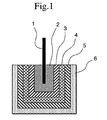
- reference number 2 denotes the anode in which the anode lead 1 stands upright
- reference number 3 denotes the dielectric coat
- reference number 4 denotes the solid electrolyte layer comprising a conductive polymer
- reference number 5 denotes the conductive paste layer
- reference number 6 denotes the cathode conductive layer.
- the conductive paste layer 5 and the cathode conductive layer 6 act as a cathode.
- Conductive polymers such as dielectric materials of polypyrrole, polythiophene, polyaniline, polyfuran, and the like can be used to the solid electrolyte layer 4.
- polypyrrole is preferable because of its stability.
- the conductive paste layer 5 is formed outside of the solid electrolyte layer 4, and prevents the contact between the outer air and the solid electrolyte layer 4, and thereby, the oxidation degradation of the solid electrolyte layer 4 can be prevented. Therefore, the conductive paste layer 5 is an important element for forming the capacitor.
- the conductive paste layer 5 uses acrylic resins as a main component mixed with cellulose resins as the binder.
- the dispersibility of the conductive powders such as graphite and the like becomes excellent and the resistance of the conductive paste layer 5 becomes low.
- the thickness of the conductive paste layer 5 is set in a range of 20 ⁇ m to 40 ⁇ m. Thereby, the cracks and peels generated when it is packed can be prevent, and the oxidation degradation of the electrolyte can be prevented; therefore, the ESR can be kept low.
- the conductive paste used in the present invention is a mixture comprising acrylic resins and cellulose resins as a binder.
- the content of cellulose resins in the binder is preferably in a range of 10 to 30 weight %. As shown in Table 2 below, when the content of cellulose resins is less than 10 weight %, the dispersibility of the conductive powders such as graphite and the like becomes low; therefore, the ESR tends to be high. In contrast, when the content of cellulose resins is more than 30 weight %, cracks and peels are generated in the conductive paste layer 5 by heat stress generated during packing, and the oxygen access channels are easily formed therein: therefore, the solid electrolyte layer 4 is easily oxidation degraded. As a result, the ESR tends to be high.
- the thickness of the conductive paste layer 5 is preferably in a range of 20 to 40 ⁇ m, because the conductive paste layer 5 having a thickness in this range has a mitigation effect for heat stress generated when it is packed.
- acrylic resins can be used as the acrylic resins comprising the conductive paste layer 5; however, methyl polymethacrylate and ethyl polymethacrylate are preferable.
- acrylic resins comprising copolymers other than these acrylic copolymers can be used as long as the effects obtained by the present invention can be obtained.
- Acrylic resins used for molding materials are preferable considering their facilitation of production.
- the average molecular weight of acrylic resins is preferably in a range of 10,000 to 1,000,000, more preferably in a range of 50,000 to 500,000, most preferably in a range of 50,000 to 200,000.
- cellulose resins can be used as cellulose resins comprising the conductive paste layer 5; however, cellulose resins; cellulose ester resins such as nitrocellulose, acetylcellulose, acetylbutylcellulose, propionylcellulose; cellulose ether resins such as ethylcellulose; and the like are preferable. Among these cellulose resins, acetylcellulose is more preferable. Moreover, the average molecular weight of cellulose resins is preferably in a range of 10,000 to 1,000,000, more preferably in a range of 20,000 to 200,000.
- the dielectric coat 3 which comprises Ta 2 O 5 was formed onto the surface of the anode 2 in which the Ta wire stands upright, then the polypyrrole layer 4 which is the solid electrolyte layer was formed.
- Gr paste was obtained by mixing 5 weight % of the binder comprising methyl polymethacrylate and acetylcellulose at a weight ratio of 4:1, 15 weight % of graphite, and 80 weight % of pure water.
- the anode 2 laminated with the dielectric coat 3 and the polypyrrole layer 4 was dipped into the obtained Gr paste at several times to form the layer comprising Gr paste with a thickness of 30 ⁇ m onto the polypyrrole layer 4. Then, the Gr paste layer 5 was formed by curing the layer comprising Gr paste at a high temperature of 150 °C, for 30 minutes.
- the solid electrolytic capacitor was obtained by forming the Ag paste layer 6 onto the Gr paste layer 5.
- a comparative solid electrolytic capacitor was prepared in a manner identical to that of Example 1 of the present invention, except that the Gr paste layer 5 comprising methyl polymethacrylate alone, which is a conventional binder, with a thickness of 10 ⁇ m was formed.
- Example 1 The high temperature- no load test at 85 °C was carried out using the obtained solid electrolytic capacitors in Example 1 and Comparative Example, and the ESR transitions by the oxidation degradation of the solid electrolyte were compared. The results are shown in Table 1 below.
- Table 1 ESR(m ⁇ ) initial value After 250 hours After 500 hours After 750 hours After 1000 hours
- the ESR transition of the solid electrolytic capacitor in Example is small; therefore, the solid electrolytic capacitor in Example 1 has a higher reliability than that of the solid electrolytic capacitor in the Comparative Example.
- the effect of preventing the oxidation degradation of the solid electrolyte layer 4 can be obtained by the solid electrolytic capacitor in Example 1.
- the solid electrolytic capacitors were prepared in a manner identical to that of Example 1 of the present invention, except that the content of cellulose resin in the binder comprising the conductive paste layer 5 was varied in a range of 0 to 80 weight % , as shown in Table 2 below.
- ESRs and ESRs after packing means ESRs of the solid electrolytic capacitors which are fixed to the glass-epoxy substrate (thickness: 1 mm; size: 100 mm ⁇ 100 mm) with a cream solder, and passed through a Reflow Oven having a temperature profile type which can maintain a temperature at 240 °C for 10 seconds.
- the results are shown in Table 2 below.
- Table 2 The content of cellulose in the binder (weight %) 0 10 20 30 40 50 60 70 80
- packing m ⁇ 300 180 175 180 200 240 280 300 350
- the content of cellulose resins in the binder is preferably in a range of 10 to 30 weight %.
- the solid electrolytic capacitors were prepared in a manner identical to that of Example 1 of the present invention, except that the thickness of the Gr paste layer 5 was varied in a range of 10 to 50 ⁇ m as shown in Table 3 below.
- ESRs after packing means the ESRs of the solid electrolytic capacitors which are fixed to the glass-epoxy substrate (thickness: 1 mm; size: 100 mm ⁇ 100 mm) with a cream solder, and passed through a Reflow Oven having a temperature profile type which can maintain a temperature at 240 °C for 10 seconds.
- Table 3 The thickness of the Gr paste layer ( ⁇ m) 10 20 30 40 50
- the thickness of the Gr paste layer 5, that is, conductive paste layer 5, is preferably in a range of 20 to 40 ⁇ m.
Landscapes
- Engineering & Computer Science (AREA)
- Power Engineering (AREA)
- Chemical & Material Sciences (AREA)
- Microelectronics & Electronic Packaging (AREA)
- Materials Engineering (AREA)
- Chemical Kinetics & Catalysis (AREA)
- Electrochemistry (AREA)
- Compositions Of Macromolecular Compounds (AREA)
Applications Claiming Priority (2)
| Application Number | Priority Date | Filing Date | Title |
|---|---|---|---|
| JP10101186A JP3080922B2 (ja) | 1998-04-13 | 1998-04-13 | 固体電解コンデンサ及びその製造方法 |
| JP10118698 | 1998-04-13 |
Publications (3)
| Publication Number | Publication Date |
|---|---|
| EP0952593A2 true EP0952593A2 (de) | 1999-10-27 |
| EP0952593A3 EP0952593A3 (de) | 2002-01-16 |
| EP0952593B1 EP0952593B1 (de) | 2010-06-23 |
Family
ID=14293957
Family Applications (1)
| Application Number | Title | Priority Date | Filing Date |
|---|---|---|---|
| EP99107022A Expired - Lifetime EP0952593B1 (de) | 1998-04-13 | 1999-04-09 | Festelektrolytkondensator und dessen Hestellungsverfahren |
Country Status (5)
| Country | Link |
|---|---|
| US (1) | US6212064B1 (de) |
| EP (1) | EP0952593B1 (de) |
| JP (1) | JP3080922B2 (de) |
| KR (1) | KR100310267B1 (de) |
| DE (1) | DE69942519D1 (de) |
Cited By (1)
| Publication number | Priority date | Publication date | Assignee | Title |
|---|---|---|---|---|
| CN101479819B (zh) * | 2006-06-27 | 2012-08-22 | 昭和电工株式会社 | 固体电解电容器 |
Families Citing this family (21)
| Publication number | Priority date | Publication date | Assignee | Title |
|---|---|---|---|---|
| JP3881480B2 (ja) * | 1999-10-14 | 2007-02-14 | ローム株式会社 | 固体電解コンデンサおよびその製法 |
| US6284555B1 (en) * | 2000-05-23 | 2001-09-04 | Vishay Sprague, Inc. | Capacitor mold and method for using same |
| US6449140B1 (en) * | 2000-07-07 | 2002-09-10 | Showa Denko K.K. | Solid electrolytic capacitor element and method for producing the same |
| JP2003197468A (ja) | 2001-10-19 | 2003-07-11 | Nec Tokin Toyama Ltd | 固体電解コンデンサ及びその製造方法 |
| DE10155393A1 (de) | 2001-11-10 | 2003-05-22 | Philips Corp Intellectual Pty | Planarer Polymer-Kondensator |
| JP4328483B2 (ja) * | 2001-11-26 | 2009-09-09 | Necトーキン株式会社 | 固体電解コンデンサ及びその製造方法 |
| JPWO2005032785A1 (ja) * | 2003-09-30 | 2007-11-15 | Tdk株式会社 | 積層セラミック電子部品用の誘電体ペーストの製造方法 |
| JP4487542B2 (ja) * | 2003-11-27 | 2010-06-23 | Tdk株式会社 | 積層セラミック電子部品用の導電体ペーストおよび積層セラミック電子部品用の積層体ユニットの製造方法 |
| JP4662298B2 (ja) * | 2003-12-15 | 2011-03-30 | Tdk株式会社 | 積層セラミック電子部品のスペーサ層用の誘電体ペースト |
| JP4487596B2 (ja) * | 2004-02-27 | 2010-06-23 | Tdk株式会社 | 積層セラミック電子部品用の積層体ユニットの製造方法 |
| JP4487595B2 (ja) * | 2004-02-27 | 2010-06-23 | Tdk株式会社 | 積層セラミック電子部品用の積層体ユニットの製造方法 |
| US7085127B2 (en) * | 2004-03-02 | 2006-08-01 | Vishay Sprague, Inc. | Surface mount chip capacitor |
| JP4412013B2 (ja) * | 2004-03-16 | 2010-02-10 | Tdk株式会社 | 積層セラミック電子部品用の誘電体ペーストおよび積層セラミック電子部品用の積層体ユニットの製造方法 |
| JP4508945B2 (ja) * | 2005-05-26 | 2010-07-21 | 三洋電機株式会社 | 固体電解コンデンサおよびその製造方法 |
| JP2007142160A (ja) * | 2005-11-18 | 2007-06-07 | Nec Tokin Corp | チップ型固体電解コンデンサ |
| JP2009209259A (ja) * | 2008-03-04 | 2009-09-17 | Nec Tokin Corp | 導電性高分子およびそれを用いた固体電解コンデンサ |
| JP5267586B2 (ja) * | 2011-01-28 | 2013-08-21 | 株式会社村田製作所 | 固体電解コンデンサおよびその製造方法 |
| US8300387B1 (en) * | 2011-04-07 | 2012-10-30 | Avx Corporation | Hermetically sealed electrolytic capacitor with enhanced mechanical stability |
| CN104916444A (zh) * | 2015-06-19 | 2015-09-16 | 深圳市金富康电子有限公司 | 一种卷绕型固体铝电解电容器的制备方法 |
| US11915884B2 (en) | 2019-08-08 | 2024-02-27 | Panasonic Intellectual Property Management Co., Ltd. | Electrolytic capacitor |
| CN115136267B (zh) * | 2020-02-28 | 2024-12-10 | 松下知识产权经营株式会社 | 电解电容器及电解电容器的导电层形成用糊剂 |
Family Cites Families (9)
| Publication number | Priority date | Publication date | Assignee | Title |
|---|---|---|---|---|
| US3337429A (en) * | 1964-05-28 | 1967-08-22 | Union Carbide Corp | Solid electrolytic capacitor and process therefor |
| US3538395A (en) * | 1968-03-12 | 1970-11-03 | Union Carbide Corp | Solid electrolyte capacitor and method for making same |
| US3823347A (en) * | 1972-04-19 | 1974-07-09 | Nat Components Ind Inc | Solid electrolytic capacitor |
| JPS5739042B2 (de) * | 1974-03-26 | 1982-08-19 | ||
| US5005107A (en) * | 1988-12-07 | 1991-04-02 | Matsushita Electric Industrial Co., Ltd. | Solid electrolytic capacitor |
| JP2637207B2 (ja) | 1988-12-21 | 1997-08-06 | 昭和電工株式会社 | 固体電解コンデンサ |
| DE69513128T2 (de) * | 1994-11-25 | 2000-06-15 | Nec Corp., Tokio/Tokyo | Festelektrolytkondensator mit zwei Elektrolytschichten und Herstellungsverfahren |
| JP3085111B2 (ja) | 1994-12-09 | 2000-09-04 | 日本電気株式会社 | 固体電解コンデンサ |
| FR2729009B1 (fr) * | 1994-12-28 | 1997-01-31 | Accumulateurs Fixes | Electrode bifonctionnelle pour generateur electrochimique ou supercondensateur et son procede de fabrication |
-
1998
- 1998-04-13 JP JP10101186A patent/JP3080922B2/ja not_active Expired - Lifetime
-
1999
- 1999-04-08 US US09/288,501 patent/US6212064B1/en not_active Expired - Lifetime
- 1999-04-09 DE DE69942519T patent/DE69942519D1/de not_active Expired - Lifetime
- 1999-04-09 EP EP99107022A patent/EP0952593B1/de not_active Expired - Lifetime
- 1999-04-12 KR KR1019990012875A patent/KR100310267B1/ko not_active Expired - Fee Related
Cited By (1)
| Publication number | Priority date | Publication date | Assignee | Title |
|---|---|---|---|---|
| CN101479819B (zh) * | 2006-06-27 | 2012-08-22 | 昭和电工株式会社 | 固体电解电容器 |
Also Published As
| Publication number | Publication date |
|---|---|
| KR100310267B1 (ko) | 2001-11-09 |
| EP0952593B1 (de) | 2010-06-23 |
| JPH11297574A (ja) | 1999-10-29 |
| DE69942519D1 (de) | 2010-08-05 |
| KR19990083142A (ko) | 1999-11-25 |
| JP3080922B2 (ja) | 2000-08-28 |
| US6212064B1 (en) | 2001-04-03 |
| EP0952593A3 (de) | 2002-01-16 |
Similar Documents
| Publication | Publication Date | Title |
|---|---|---|
| EP0952593B1 (de) | Festelektrolytkondensator und dessen Hestellungsverfahren | |
| EP2290664B1 (de) | Festelektrolytkondensator und Herstellungsverfahren dafür | |
| KR101525258B1 (ko) | 고체 전해 콘덴서의 제조 방법 | |
| EP0714108B1 (de) | Festelektrolytkondensator mit zwei Elektrolytschichten und Herstellungsverfahren | |
| CN1111884C (zh) | 固体电解质电容器及其制造方法 | |
| US20030218859A1 (en) | Anode Member for a solid electrolytic capacitor, method of producing the same and solid electrolytic capacitor using the same | |
| US10079112B2 (en) | Method for producing electrolytic capacitor | |
| EP0899757B1 (de) | Herstellungsverfahren für einen Festelektrolytkondensator wobei ein organisches leitendes Polymer verwendet wird | |
| EP1876612B1 (de) | Festelektrolyt-kondensatorelement, herstellungsverfahren dafür und festelektrolyt-kondensator | |
| US20090089990A1 (en) | Method for manufacturing solid electrolytic capacitor | |
| EP1898433B1 (de) | Festelektrolytkondensator und dessen herstellungsverfahren | |
| EP1768140A1 (de) | Kondensatorelement und kohlenstoffpaste | |
| CN1930647A (zh) | 固体电解电容器及其用途 | |
| US7876548B2 (en) | Niobium solid electrolytic capacitor and its production method | |
| JP3391364B2 (ja) | タンタル固体電解コンデンサの製造方法 | |
| EP0607781A1 (de) | Festelektrolytkondensator | |
| JP4451235B2 (ja) | 固体電解コンデンサの製造方法 | |
| CN1823397B (zh) | 制造固体电解电容器的方法 | |
| US20090090997A1 (en) | Solid electrolytic capacitor element and production method thereof | |
| US20090190287A1 (en) | Solid electrolytic capacitor and manufacturing method thereof | |
| JP2006339182A (ja) | 固体電解コンデンサ | |
| JPH03256313A (ja) | アルミニウム固体電解コンデンサ | |
| KR20100031459A (ko) | 고주파영역에서의 임피던스가 충분히 낮은 고체 전해 콘덴서의 제조방법 |
Legal Events
| Date | Code | Title | Description |
|---|---|---|---|
| PUAI | Public reference made under article 153(3) epc to a published international application that has entered the european phase |
Free format text: ORIGINAL CODE: 0009012 |
|
| AK | Designated contracting states |
Kind code of ref document: A2 Designated state(s): AT BE CH CY DE DK ES FI FR GB GR IE IT LI LU MC NL PT SE Kind code of ref document: A2 Designated state(s): DE GB |
|
| AX | Request for extension of the european patent |
Free format text: AL;LT;LV;MK;RO;SI |
|
| PUAL | Search report despatched |
Free format text: ORIGINAL CODE: 0009013 |
|
| AK | Designated contracting states |
Kind code of ref document: A3 Designated state(s): AT BE CH CY DE DK ES FI FR GB GR IE IT LI LU MC NL PT SE |
|
| AX | Request for extension of the european patent |
Free format text: AL;LT;LV;MK;RO;SI |
|
| 17P | Request for examination filed |
Effective date: 20011203 |
|
| RAP1 | Party data changed (applicant data changed or rights of an application transferred) |
Owner name: NEC TOKIN TOYAMA, LTD. |
|
| AKX | Designation fees paid |
Free format text: DE GB |
|
| GRAP | Despatch of communication of intention to grant a patent |
Free format text: ORIGINAL CODE: EPIDOSNIGR1 |
|
| GRAJ | Information related to disapproval of communication of intention to grant by the applicant or resumption of examination proceedings by the epo deleted |
Free format text: ORIGINAL CODE: EPIDOSDIGR1 |
|
| GRAP | Despatch of communication of intention to grant a patent |
Free format text: ORIGINAL CODE: EPIDOSNIGR1 |
|
| GRAS | Grant fee paid |
Free format text: ORIGINAL CODE: EPIDOSNIGR3 |
|
| GRAA | (expected) grant |
Free format text: ORIGINAL CODE: 0009210 |
|
| AK | Designated contracting states |
Kind code of ref document: B1 Designated state(s): DE GB |
|
| REF | Corresponds to: |
Ref document number: 69942519 Country of ref document: DE Date of ref document: 20100805 Kind code of ref document: P |
|
| PLBE | No opposition filed within time limit |
Free format text: ORIGINAL CODE: 0009261 |
|
| STAA | Information on the status of an ep patent application or granted ep patent |
Free format text: STATUS: NO OPPOSITION FILED WITHIN TIME LIMIT |
|
| 26N | No opposition filed |
Effective date: 20110324 |
|
| REG | Reference to a national code |
Ref country code: DE Ref legal event code: R097 Ref document number: 69942519 Country of ref document: DE Effective date: 20110323 |
|
| PGFP | Annual fee paid to national office [announced via postgrant information from national office to epo] |
Ref country code: DE Payment date: 20120425 Year of fee payment: 14 |
|
| PGFP | Annual fee paid to national office [announced via postgrant information from national office to epo] |
Ref country code: GB Payment date: 20120404 Year of fee payment: 14 |
|
| GBPC | Gb: european patent ceased through non-payment of renewal fee |
Effective date: 20130409 |
|
| PG25 | Lapsed in a contracting state [announced via postgrant information from national office to epo] |
Ref country code: GB Free format text: LAPSE BECAUSE OF NON-PAYMENT OF DUE FEES Effective date: 20130409 Ref country code: DE Free format text: LAPSE BECAUSE OF NON-PAYMENT OF DUE FEES Effective date: 20131101 |
|
| REG | Reference to a national code |
Ref country code: DE Ref legal event code: R119 Ref document number: 69942519 Country of ref document: DE Effective date: 20131101 |