EP0953856A2 - Lötfreie optische Packung - Google Patents
Lötfreie optische Packung Download PDFInfo
- Publication number
- EP0953856A2 EP0953856A2 EP99303034A EP99303034A EP0953856A2 EP 0953856 A2 EP0953856 A2 EP 0953856A2 EP 99303034 A EP99303034 A EP 99303034A EP 99303034 A EP99303034 A EP 99303034A EP 0953856 A2 EP0953856 A2 EP 0953856A2
- Authority
- EP
- European Patent Office
- Prior art keywords
- package according
- printed circuit
- circuit board
- base member
- board
- Prior art date
- Legal status (The legal status is an assumption and is not a legal conclusion. Google has not performed a legal analysis and makes no representation as to the accuracy of the status listed.)
- Withdrawn
Links
- 230000003287 optical effect Effects 0.000 title claims abstract description 17
- 229920001169 thermoplastic Polymers 0.000 claims 2
- 239000004416 thermosoftening plastic Substances 0.000 claims 2
- 238000005476 soldering Methods 0.000 abstract description 2
- 239000000463 material Substances 0.000 description 3
- 229910000679 solder Inorganic materials 0.000 description 3
- 238000000034 method Methods 0.000 description 2
- 230000005693 optoelectronics Effects 0.000 description 2
- 238000003491 array Methods 0.000 description 1
- 238000004140 cleaning Methods 0.000 description 1
- 230000004907 flux Effects 0.000 description 1
- 238000003780 insertion Methods 0.000 description 1
- 230000037431 insertion Effects 0.000 description 1
- 239000013307 optical fiber Substances 0.000 description 1
- 238000004806 packaging method and process Methods 0.000 description 1
- 238000012856 packing Methods 0.000 description 1
- 239000004033 plastic Substances 0.000 description 1
- 238000007747 plating Methods 0.000 description 1
- 239000012815 thermoplastic material Substances 0.000 description 1
Images


Classifications
-
- H—ELECTRICITY
- H05—ELECTRIC TECHNIQUES NOT OTHERWISE PROVIDED FOR
- H05K—PRINTED CIRCUITS; CASINGS OR CONSTRUCTIONAL DETAILS OF ELECTRIC APPARATUS; MANUFACTURE OF ASSEMBLAGES OF ELECTRICAL COMPONENTS
- H05K5/00—Casings, cabinets or drawers for electric apparatus
- H05K5/0091—Housing specially adapted for small components
-
- G—PHYSICS
- G02—OPTICS
- G02B—OPTICAL ELEMENTS, SYSTEMS OR APPARATUS
- G02B6/00—Light guides; Structural details of arrangements comprising light guides and other optical elements, e.g. couplings
- G02B6/24—Coupling light guides
- G02B6/42—Coupling light guides with opto-electronic elements
- G02B6/4201—Packages, e.g. shape, construction, internal or external details
- G02B6/4256—Details of housings
- G02B6/426—Details of housings mounting, engaging or coupling of the package to a board, a frame or a panel
- G02B6/4261—Packages with mounting structures to be pluggable or detachable, e.g. having latches or rails
-
- G—PHYSICS
- G02—OPTICS
- G02B—OPTICAL ELEMENTS, SYSTEMS OR APPARATUS
- G02B6/00—Light guides; Structural details of arrangements comprising light guides and other optical elements, e.g. couplings
- G02B6/24—Coupling light guides
- G02B6/42—Coupling light guides with opto-electronic elements
- G02B6/4201—Packages, e.g. shape, construction, internal or external details
- G02B6/4274—Electrical aspects
- G02B6/4284—Electrical aspects of optical modules with disconnectable electrical connectors
-
- G—PHYSICS
- G02—OPTICS
- G02B—OPTICAL ELEMENTS, SYSTEMS OR APPARATUS
- G02B6/00—Light guides; Structural details of arrangements comprising light guides and other optical elements, e.g. couplings
- G02B6/24—Coupling light guides
- G02B6/42—Coupling light guides with opto-electronic elements
- G02B6/4292—Coupling light guides with opto-electronic elements the light guide being disconnectable from the opto-electronic element, e.g. mutually self aligning arrangements
-
- G—PHYSICS
- G02—OPTICS
- G02B—OPTICAL ELEMENTS, SYSTEMS OR APPARATUS
- G02B6/00—Light guides; Structural details of arrangements comprising light guides and other optical elements, e.g. couplings
- G02B6/24—Coupling light guides
- G02B6/42—Coupling light guides with opto-electronic elements
- G02B6/4201—Packages, e.g. shape, construction, internal or external details
- G02B6/4274—Electrical aspects
- G02B6/428—Electrical aspects containing printed circuit boards [PCB]
Definitions
- This invention relates to optoelectronics, and in particular to a package for optical components.
- Optoelectronic packaging in general, and optical transceiver modules in particular, are being driven by the need for higher packing densities and lower costs.
- One way of simplifying the assembly process, and thereby reduce the cost, is to eliminate the need for solder attachment of the leads providing electrical connection to the components in the package, since solder attachment requires extra processing steps such as fluxing and cleaning the flux and the cost of equipment associated with such processes.
- the invention is an optical package including a dielectric housing for enclosing optical components, the housing including sidewalls and an opening. At least one printed circuit board including at least one metalized pad is mounted to one of the sidewalls.
- a base member includes at least one lead inserted therein. The base member is shaped to provide a snap fit with the sidewalls at the opening so that a portion of the lead is spring-loaded onto the contact pad to provide electrical contact with the board.
- Figs 1 illustrates the assembling of the package, 10, and Fig 2 illustrates the assembled package, 10, in accordance with an exemplary embodiment.
- the package, 10, includes a dielectric housing, 11, for enclosing optical components, 12 and 13, the housing including sidewalls, 14 and 15, and an opening, 16.
- At least one printed circuit board, 17 or 18, including at least one metalized pad, 19 or 20, is mounted to one of the sidewalls, 14 or 15.
- a base member, 30, includes at least one lead, 31 or 32, insert-molded or press fit therein.
- the base member is shaped to provide a press fit with the sidewalls, 14 and 15, at the opening, 16, so that a portion of the lead, 31 or 32, is spring-loaded onto the metalized pad, 19 or 20, to provide low resistance electrical contact with the board 17 or 18.
- the dielectric housing, 11, is typically a high temperature thermoplastic material.
- Each pin, 21 and 22, is designed to mate with a corresponding hole, 23 and 24, in the circuit board, 17 and 18, so that the board can be mounted securely to its corresponding sidewall by a snap-on action.
- the optical component, 12, in this example, is a laser such as a 1310nm MQW edge emitting laser sold under the designation Lucent 370-type laser, and the optical component, 13, is a photodetector, such as a preamplifier and pin sold under the designation Lucent 170-type detector, so that the package, 10, comprises a transceiver.
- a laser such as a 1310nm MQW edge emitting laser sold under the designation Lucent 370-type laser
- the optical component, 13 is a photodetector, such as a preamplifier and pin sold under the designation Lucent 170-type detector, so that the package, 10, comprises a transceiver.
- Other types of optical components can be employed.
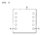
- the sidewalls , 14 and 15, further include grooves, 25 and 26, positioned near the opening 16.
- the grooves are V-shaped, but other configurations are possible.
- the edges, 33 and 34, of the base member, 30, are beveled so as to fit within the grooves, 25 and 26, respectively.
- the base member, 30, is also mounted to the sidewalls, 14 and 15, by a snap action.
- the base member, 30, can also be a plastic material which is the same as or different from the material of the housing, 11.
- the conductive leads, 31 and 32 are typically made of BeCu selectively plated with Au. Solder plating, not shown, may also be applied to the surfaces of the leads for attachment to a mother board, also not shown.
- the leads, e.g. 31 and 32 are insert-molded or press fit within corresponding holes, e.g., 35 and 36, through the member.
- the holes, e.g., 35 and 36 are formed in two arrays near respective edges of the member, 30.
- the position of the holes, e.g., 35 and 36, and the material of the leads , e.g., 31 and 32, ensures that when the base member, 30, is snapped onto the sidewalls, 14 and 15, the leads, e.g. 31 and 32 will exert a spring force against their corresponding pads, e.g., 19 and 20, respectively, to provide robust electrical contact.
- the base member, 30, can include printed circuitry (not shown) on a major surface thereof in addition to the leads, 31 and 32.
- Fig 4 illustrates in a schematic plan view one example of a hybrid integrated circuit, 40, which can be enclosed within the package, 10.
- the hybrid circuit, 40 in this example is a transmitter circuit which includes the laser, 12, mounted near one end of the printed circuit board, 17, and extending in front of it, and electronic circuitry, illustrated by block 41, which comprises the laser drive circuitry, formed on the remainder of the board.
- a plurality of conductive leads, e.g., 31, is coupled to respective metalized pads, e.g. 19, as described previously to provide electrical connection to the circuitry, 41, which in turn drives the laser, 12.
- a standard type of optical connector receptacle, 42 such as an LC-type receptacle, is molded as an integral part of the housing 11.
- the receptacle, 42 includes an optical port, 43, for receiving an optical connector, 44, which connects to an optical fiber 45, so that light from the laser can be transmitted.
- a mounting post, 46, extending from the circuit board may also be provided for insertion in the mother board to relieve stress on the components.
- a similar hybrid circuit can be mounted to the other sidewall, with the laser, 12, replaced by a photodetector (13 of Fig 1) so as to form a transceiver package.
Landscapes
- Physics & Mathematics (AREA)
- General Physics & Mathematics (AREA)
- Optics & Photonics (AREA)
- Engineering & Computer Science (AREA)
- Microelectronics & Electronic Packaging (AREA)
- Led Device Packages (AREA)
- Optical Couplings Of Light Guides (AREA)
Applications Claiming Priority (2)
| Application Number | Priority Date | Filing Date | Title |
|---|---|---|---|
| US6912898A | 1998-04-29 | 1998-04-29 | |
| US69128 | 1998-04-29 |
Publications (2)
| Publication Number | Publication Date |
|---|---|
| EP0953856A2 true EP0953856A2 (de) | 1999-11-03 |
| EP0953856A3 EP0953856A3 (de) | 2000-04-05 |
Family
ID=22086926
Family Applications (1)
| Application Number | Title | Priority Date | Filing Date |
|---|---|---|---|
| EP99303034A Withdrawn EP0953856A3 (de) | 1998-04-29 | 1999-04-20 | Lötfreie optische Packung |
Country Status (1)
| Country | Link |
|---|---|
| EP (1) | EP0953856A3 (de) |
Cited By (2)
| Publication number | Priority date | Publication date | Assignee | Title |
|---|---|---|---|---|
| EP1298472A1 (de) * | 2001-09-27 | 2003-04-02 | Agilent Technologies, Inc. (a Delaware corporation) | Gehäuse für opto-elektrischen Komponenten |
| WO2015017243A1 (en) * | 2013-08-02 | 2015-02-05 | Fci Asia Pte. Ltd | Opto-electrical transceiver module and active optical cable |
Family Cites Families (4)
| Publication number | Priority date | Publication date | Assignee | Title |
|---|---|---|---|---|
| US3575546A (en) * | 1970-02-24 | 1971-04-20 | James P Liautaud | Header and shell encasement for electronic components and the like |
| US3737729A (en) * | 1971-06-14 | 1973-06-05 | Zeltex Inc | Electronic package and method of construction |
| US4106842A (en) * | 1976-09-23 | 1978-08-15 | Gte Sylvania Incorporated | Electrical contact and connector |
| JP3326959B2 (ja) * | 1994-04-25 | 2002-09-24 | 松下電器産業株式会社 | 光ファイバモジュール |
-
1999
- 1999-04-20 EP EP99303034A patent/EP0953856A3/de not_active Withdrawn
Cited By (4)
| Publication number | Priority date | Publication date | Assignee | Title |
|---|---|---|---|---|
| EP1298472A1 (de) * | 2001-09-27 | 2003-04-02 | Agilent Technologies, Inc. (a Delaware corporation) | Gehäuse für opto-elektrischen Komponenten |
| US6783393B2 (en) | 2001-09-27 | 2004-08-31 | Agilent Technologies, Inc. | Package for opto-electrical components |
| WO2015017243A1 (en) * | 2013-08-02 | 2015-02-05 | Fci Asia Pte. Ltd | Opto-electrical transceiver module and active optical cable |
| US9638876B2 (en) | 2013-08-02 | 2017-05-02 | Fci Americas Technology Llc | Opto-electrical transceiver module and active optical cable |
Also Published As
| Publication number | Publication date |
|---|---|
| EP0953856A3 (de) | 2000-04-05 |
Similar Documents
| Publication | Publication Date | Title |
|---|---|---|
| US5611013A (en) | Optical miniature capsule | |
| JP2562217B2 (ja) | 光通信集成装置 | |
| EP0437931B1 (de) | Gehäuse für ein Paar von optischen Vorrichtungen | |
| US5940562A (en) | Stubless optoelectronic device receptacle | |
| US6969280B2 (en) | Electrical connector with double mating interfaces for electronic components | |
| EP0600645B1 (de) | Elektro-optischer Baustein mit linear angeordneten Komponenten | |
| US5539200A (en) | Integrated optoelectronic substrate | |
| US6994480B2 (en) | Optical link module | |
| US7625133B2 (en) | Method of assembling optoelectronic devices and an optoelectronic device assembled according to this method | |
| US6024500A (en) | Transceiver package | |
| US6565384B2 (en) | Electro-optical connector with flexible circuit | |
| US6863451B2 (en) | Optical module | |
| US7004646B2 (en) | Receptacle type optical transmitter and/or receiver module | |
| EP0953856A2 (de) | Lötfreie optische Packung | |
| US6833999B2 (en) | Optical module and method of making the same | |
| US6530699B1 (en) | Dual channel device having two optical sub-assemblies | |
| JP2001337249A (ja) | 光通信用レセプタクル | |
| US7699618B2 (en) | Optical transceiver with an FPC board connecting an optical subassembly with a circuit board | |
| US6457876B1 (en) | Surface-mountable optical device | |
| US20070047882A1 (en) | Shaped lead assembly for optoelectronic devices | |
| US6783393B2 (en) | Package for opto-electrical components | |
| JPH11202163A (ja) | 光リンク装置 | |
| JPH0968630A (ja) | 光ファイバコネクタおよびその固定方法 | |
| JP2003084174A (ja) | 発光モジュール及び受光モジュール | |
| US20150323749A1 (en) | Surface mount device (smd) optical port |
Legal Events
| Date | Code | Title | Description |
|---|---|---|---|
| PUAI | Public reference made under article 153(3) epc to a published international application that has entered the european phase |
Free format text: ORIGINAL CODE: 0009012 |
|
| AK | Designated contracting states |
Kind code of ref document: A2 Designated state(s): AT BE CH CY DE DK ES FI FR GB GR IE IT LI LU MC NL PT SE |
|
| AX | Request for extension of the european patent |
Free format text: AL;LT;LV;MK;RO;SI |
|
| PUAL | Search report despatched |
Free format text: ORIGINAL CODE: 0009013 |
|
| AK | Designated contracting states |
Kind code of ref document: A3 Designated state(s): AT BE CH CY DE DK ES FI FR GB GR IE IT LI LU MC NL PT SE |
|
| AX | Request for extension of the european patent |
Free format text: AL;LT;LV;MK;RO;SI |
|
| AKX | Designation fees paid | ||
| STAA | Information on the status of an ep patent application or granted ep patent |
Free format text: STATUS: THE APPLICATION IS DEEMED TO BE WITHDRAWN |
|
| 18D | Application deemed to be withdrawn |
Effective date: 20001006 |