EP0954005B1 - Verfahren zur Herstellung einer Elektronenquelle und eines Bilderzeugungsgeräts - Google Patents
Verfahren zur Herstellung einer Elektronenquelle und eines Bilderzeugungsgeräts Download PDFInfo
- Publication number
- EP0954005B1 EP0954005B1 EP99303346A EP99303346A EP0954005B1 EP 0954005 B1 EP0954005 B1 EP 0954005B1 EP 99303346 A EP99303346 A EP 99303346A EP 99303346 A EP99303346 A EP 99303346A EP 0954005 B1 EP0954005 B1 EP 0954005B1
- Authority
- EP
- European Patent Office
- Prior art keywords
- voltage
- wirings
- group
- forming
- direction wirings
- Prior art date
- Legal status (The legal status is an assumption and is not a legal conclusion. Google has not performed a legal analysis and makes no representation as to the accuracy of the status listed.)
- Expired - Lifetime
Links
- 238000004519 manufacturing process Methods 0.000 title claims description 23
- 238000000034 method Methods 0.000 claims description 183
- 239000000758 substrate Substances 0.000 claims description 74
- 239000007789 gas Substances 0.000 claims description 22
- 230000015572 biosynthetic process Effects 0.000 claims description 11
- 230000004913 activation Effects 0.000 claims description 10
- 239000000126 substance Substances 0.000 claims description 9
- OKTJSMMVPCPJKN-UHFFFAOYSA-N Carbon Chemical compound [C] OKTJSMMVPCPJKN-UHFFFAOYSA-N 0.000 claims description 5
- 229910052799 carbon Inorganic materials 0.000 claims description 5
- UFHFLCQGNIYNRP-UHFFFAOYSA-N Hydrogen Chemical compound [H][H] UFHFLCQGNIYNRP-UHFFFAOYSA-N 0.000 claims description 2
- 229910052739 hydrogen Inorganic materials 0.000 claims 1
- 239000001257 hydrogen Substances 0.000 claims 1
- 230000008569 process Effects 0.000 description 96
- 239000010408 film Substances 0.000 description 55
- 238000001994 activation Methods 0.000 description 24
- 229910052751 metal Inorganic materials 0.000 description 16
- 239000002184 metal Substances 0.000 description 14
- 239000010410 layer Substances 0.000 description 13
- 238000010586 diagram Methods 0.000 description 10
- 239000011521 glass Substances 0.000 description 10
- VYPSYNLAJGMNEJ-UHFFFAOYSA-N Silicium dioxide Chemical compound O=[Si]=O VYPSYNLAJGMNEJ-UHFFFAOYSA-N 0.000 description 9
- 239000010409 thin film Substances 0.000 description 8
- 150000001875 compounds Chemical class 0.000 description 7
- 239000000463 material Substances 0.000 description 7
- 239000012298 atmosphere Substances 0.000 description 6
- JFDZBHWFFUWGJE-UHFFFAOYSA-N benzonitrile Chemical compound N#CC1=CC=CC=C1 JFDZBHWFFUWGJE-UHFFFAOYSA-N 0.000 description 6
- 239000011159 matrix material Substances 0.000 description 6
- 230000006378 damage Effects 0.000 description 5
- 230000007423 decrease Effects 0.000 description 5
- 239000004615 ingredient Substances 0.000 description 5
- 238000007639 printing Methods 0.000 description 5
- 238000007789 sealing Methods 0.000 description 5
- 229910052681 coesite Inorganic materials 0.000 description 4
- 229910052906 cristobalite Inorganic materials 0.000 description 4
- 238000009826 distribution Methods 0.000 description 4
- 239000000203 mixture Substances 0.000 description 4
- 238000000206 photolithography Methods 0.000 description 4
- 238000007650 screen-printing Methods 0.000 description 4
- 239000000377 silicon dioxide Substances 0.000 description 4
- 239000005361 soda-lime glass Substances 0.000 description 4
- 229910052682 stishovite Inorganic materials 0.000 description 4
- XOLBLPGZBRYERU-UHFFFAOYSA-N tin dioxide Chemical compound O=[Sn]=O XOLBLPGZBRYERU-UHFFFAOYSA-N 0.000 description 4
- 229910052905 tridymite Inorganic materials 0.000 description 4
- 229910002674 PdO Inorganic materials 0.000 description 3
- 239000007864 aqueous solution Substances 0.000 description 3
- 238000005530 etching Methods 0.000 description 3
- 230000020169 heat generation Effects 0.000 description 3
- 150000002739 metals Chemical class 0.000 description 3
- 239000004065 semiconductor Substances 0.000 description 3
- 230000006641 stabilisation Effects 0.000 description 3
- 238000011105 stabilization Methods 0.000 description 3
- 238000007738 vacuum evaporation Methods 0.000 description 3
- -1 In2O3 and SnO2 Chemical class 0.000 description 2
- 239000006087 Silane Coupling Agent Substances 0.000 description 2
- 230000002411 adverse Effects 0.000 description 2
- 230000008901 benefit Effects 0.000 description 2
- 229910052804 chromium Inorganic materials 0.000 description 2
- 239000003086 colorant Substances 0.000 description 2
- 239000004020 conductor Substances 0.000 description 2
- 229910052802 copper Inorganic materials 0.000 description 2
- 238000000151 deposition Methods 0.000 description 2
- 230000000694 effects Effects 0.000 description 2
- 239000007772 electrode material Substances 0.000 description 2
- 238000001704 evaporation Methods 0.000 description 2
- 238000010438 heat treatment Methods 0.000 description 2
- PJXISJQVUVHSOJ-UHFFFAOYSA-N indium(III) oxide Inorganic materials [O-2].[O-2].[O-2].[In+3].[In+3] PJXISJQVUVHSOJ-UHFFFAOYSA-N 0.000 description 2
- 239000011229 interlayer Substances 0.000 description 2
- 238000005259 measurement Methods 0.000 description 2
- 150000002736 metal compounds Chemical class 0.000 description 2
- 229910044991 metal oxide Inorganic materials 0.000 description 2
- 150000004706 metal oxides Chemical class 0.000 description 2
- 238000007645 offset printing Methods 0.000 description 2
- 229910052763 palladium Inorganic materials 0.000 description 2
- 229910052697 platinum Inorganic materials 0.000 description 2
- 230000009467 reduction Effects 0.000 description 2
- 239000000243 solution Substances 0.000 description 2
- 125000006850 spacer group Chemical group 0.000 description 2
- 230000008646 thermal stress Effects 0.000 description 2
- 229910052718 tin Inorganic materials 0.000 description 2
- 229910052719 titanium Inorganic materials 0.000 description 2
- 229910052721 tungsten Inorganic materials 0.000 description 2
- 229910003862 HfB2 Inorganic materials 0.000 description 1
- 229910025794 LaB6 Inorganic materials 0.000 description 1
- ATJFFYVFTNAWJD-UHFFFAOYSA-N Tin Chemical compound [Sn] ATJFFYVFTNAWJD-UHFFFAOYSA-N 0.000 description 1
- 229910007948 ZrB2 Inorganic materials 0.000 description 1
- 229910045601 alloy Inorganic materials 0.000 description 1
- 239000000956 alloy Substances 0.000 description 1
- PNEYBMLMFCGWSK-UHFFFAOYSA-N aluminium oxide Inorganic materials [O-2].[O-2].[O-2].[Al+3].[Al+3] PNEYBMLMFCGWSK-UHFFFAOYSA-N 0.000 description 1
- GHPGOEFPKIHBNM-UHFFFAOYSA-N antimony(3+);oxygen(2-) Chemical compound [O-2].[O-2].[O-2].[Sb+3].[Sb+3] GHPGOEFPKIHBNM-UHFFFAOYSA-N 0.000 description 1
- VWZIXVXBCBBRGP-UHFFFAOYSA-N boron;zirconium Chemical compound B#[Zr]#B VWZIXVXBCBBRGP-UHFFFAOYSA-N 0.000 description 1
- 239000000919 ceramic Substances 0.000 description 1
- 239000012141 concentrate Substances 0.000 description 1
- 230000003247 decreasing effect Effects 0.000 description 1
- 239000003599 detergent Substances 0.000 description 1
- 238000007598 dipping method Methods 0.000 description 1
- 230000008020 evaporation Effects 0.000 description 1
- 239000010419 fine particle Substances 0.000 description 1
- 229910052737 gold Inorganic materials 0.000 description 1
- 230000002209 hydrophobic effect Effects 0.000 description 1
- 229910052738 indium Inorganic materials 0.000 description 1
- 239000011261 inert gas Substances 0.000 description 1
- 239000012212 insulator Substances 0.000 description 1
- 229910052742 iron Inorganic materials 0.000 description 1
- 229910052745 lead Inorganic materials 0.000 description 1
- YEXPOXQUZXUXJW-UHFFFAOYSA-N lead(II) oxide Inorganic materials [Pb]=O YEXPOXQUZXUXJW-UHFFFAOYSA-N 0.000 description 1
- 150000001247 metal acetylides Chemical class 0.000 description 1
- 229910052759 nickel Inorganic materials 0.000 description 1
- 150000004767 nitrides Chemical class 0.000 description 1
- 150000002894 organic compounds Chemical class 0.000 description 1
- 239000003960 organic solvent Substances 0.000 description 1
- 238000000059 patterning Methods 0.000 description 1
- 230000000704 physical effect Effects 0.000 description 1
- 229910021420 polycrystalline silicon Inorganic materials 0.000 description 1
- 229920005591 polysilicon Polymers 0.000 description 1
- 238000004904 shortening Methods 0.000 description 1
- 229910052710 silicon Inorganic materials 0.000 description 1
- 229910052709 silver Inorganic materials 0.000 description 1
- 238000005245 sintering Methods 0.000 description 1
- 238000005507 spraying Methods 0.000 description 1
- 238000004544 sputter deposition Methods 0.000 description 1
- 229910052715 tantalum Inorganic materials 0.000 description 1
- 238000001771 vacuum deposition Methods 0.000 description 1
- XLYOFNOQVPJJNP-UHFFFAOYSA-N water Substances O XLYOFNOQVPJJNP-UHFFFAOYSA-N 0.000 description 1
- 229910052725 zinc Inorganic materials 0.000 description 1
Images


Classifications
-
- H—ELECTRICITY
- H01—ELECTRIC ELEMENTS
- H01J—ELECTRIC DISCHARGE TUBES OR DISCHARGE LAMPS
- H01J1/00—Details of electrodes, of magnetic control means, of screens, or of the mounting or spacing thereof, common to two or more basic types of discharge tubes or lamps
- H01J1/02—Main electrodes
- H01J1/30—Cold cathodes, e.g. field-emissive cathode
-
- H—ELECTRICITY
- H01—ELECTRIC ELEMENTS
- H01J—ELECTRIC DISCHARGE TUBES OR DISCHARGE LAMPS
- H01J9/00—Apparatus or processes specially adapted for the manufacture, installation, removal, maintenance of electric discharge tubes, discharge lamps, or parts thereof; Recovery of material from discharge tubes or lamps
- H01J9/02—Manufacture of electrodes or electrode systems
- H01J9/022—Manufacture of electrodes or electrode systems of cold cathodes
- H01J9/027—Manufacture of electrodes or electrode systems of cold cathodes of thin film cathodes
-
- H—ELECTRICITY
- H01—ELECTRIC ELEMENTS
- H01J—ELECTRIC DISCHARGE TUBES OR DISCHARGE LAMPS
- H01J2329/00—Electron emission display panels, e.g. field emission display panels
Definitions
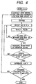
- the process of forming the film 6 containing carbon as a principal ingredient is called an "energization activation” process or simply “activation” process.
- the activation process is executed by setting, e.g., an electron-emitting device having undergone the forming process in an organic-gas-containing atmosphere and repeatedly applying a pulse voltage between a pair of device electrodes.
- This steep temperature gradient on the substrate generates thermal stress to deform or destruct in the worst case the substrate.
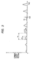
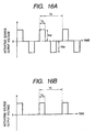
- the voltage is preferably applied to one group a plurality of the number of times at a predetermined interval.
- Step-5 Face Plate Formation Step
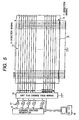
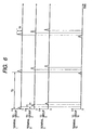
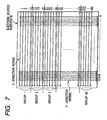
- the pulse was applied to all the remaining wirings. Note that the pulse was not simultaneously applied to respective x-direction wirings.
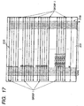
- Units constituting each group were selected at an equal interval of ((m/i)-2) (30 in Example 5) x-direction wirings. More specifically, as shown in Fig. 9, x-direction wirings 1, 2, 33, 34,..., 1+(m/i)*(i-1), and 2+(m/i)*(i-1) were selected for group 1, and x-direction wirings k, k+1, k+32, k+1+32,..., k+(m/i)*(i-1), and k+1+(m/i)*(i-1) were selected for group k.
- the duty of the forming pulse is limited by the reciprocal of the number of wirings belonging to one group. For example, to obtain a duty of 10%, the number of wirings belonging to one group must be set within 10.
Landscapes
- Engineering & Computer Science (AREA)
- Manufacturing & Machinery (AREA)
- Cold Cathode And The Manufacture (AREA)
Claims (13)
- Verfahren zur Herstellung einer Elektronenquelle, die durch eine Vielzahl von auf einem Substrat angeordneten Leiterbahnen in x-Richtung, einer Vielzahl von die Leiterbahnen in x-Richtung kreuzenden Leiterbahnen in y-Richtung, einer isolierenden Schicht zur elektrischen Isolierung der Leiterbahnen in x- und y-Richtung sowie einer Vielzahl von leitenden Schichten gebildet wird, von denen jede mit den Leiterbahnen in x- und y-Richtung verbunden ist und eine Lücke aufweist,
gekennzeichnet durch
einen Leitungsschichtausbildungsschritt für die Ausbildung einer Vielzahl von leitenden Schichten, die mit der Vielzahl von Leiterbahnen in x- und y-Richtung zu verbinden sind;
einen Gruppierungsschritt für die Zuordnung der Leiterbahnen in x-Richtung in eine Vielzahl von Gruppen; und
einen Spannungsausbildungsschritt für die sequentielle Durchführung eines Schritts bei allen Gruppen, bei dem eine Spannung an alle derselben Gruppe zugeordneten Leiterbahnen gleichzeitig angelegt wird, wodurch Lücken in den leitenden Schichten ausgebildet werden, wobei
bei dem Gruppierungsschritt
eine Vielzahl von Leiterbahnen jeder Gruppe zugeordnet werden, so dass zwischen eine Gruppe bildenden Leiterbahnen andere Gruppen bildende Leiterbahnen existieren. - Verfahren nach Anspruch 1, dadurch gekennzeichnet, dass der Ausbildungsschritt so ausgeführt wird, dass zwischen einer Gruppe zugeordneten Leiterbahnen und einer anderen Gruppe zugeordneten Leiterbahnen, an welche die Spannung im Anschluss an die erste Gruppe angelegt wird, zu einer weiteren Gruppe zugeordnete Leiterbahnen angeordnet sind.
- Verfahren nach Anspruch 1 oder 2, dadurch gekennzeichnet, dass die Spannung so angelegt wird, dass sich aufeinanderfolgende Anlegeperioden zwischen Gruppen nicht überlappen.
- Verfahren nach einem der Ansprüche 1 bis 3, dadurch gekennzeichnet, dass die Spannung an eine Gruppe mit einem vorbestimmten Intervall mehrfach angelegt wird.
- Verfahren nach Anspruch 4, dadurch gekennzeichnet, dass die Spannung an die verbleibenden Gruppen während des Intervalls zum Anlegen der Spannung an eine Gruppe angelegt wird.
- Verfahren nach Anspruch 4, dadurch gekennzeichnet, dass die Anlegespannung zumindest zwei Spannungswerte beinhaltet.
- Verfahren nach Anspruch 6, dadurch gekennzeichnet, dass sich der Spannungswert graduell erhöht.
- Verfahren nach Anspruch 4, dadurch gekennzeichnet, dass die Anlegespannung einen Konstantwert aufweist.
- Verfahren nach einem der Ansprüche 1 bis 8, dadurch gekennzeichnet, dass die leitende Schicht aus einem Oxid ausgebildet wird, und der Ausbildungsschritt durchgeführt wird, während ein Gas zur Reduktion des Oxids in Kontakt mit der leitenden Schicht gebracht wird.
- Verfahren nach Anspruch 9, dadurch gekennzeichnet, dass das reduzierende Gas Wasserstoff enthält.
- Verfahren nach einem der Ansprüche 1 bis 10, gekennzeichnet durch einen zusätzlichen Aktivierungsschritt für das Anlegung der Spannung an jede leitende Schicht, während ein eine organische Substanz enthaltendes Gas in die Nähe der Lücke gebracht wird, wodurch eine Kohlenstoffschicht auf der leitenden Schicht in der Nähe der Lücke ausgebildet wird.
- Verfahren nach Anspruch 11, dadurch gekennzeichnet, dass die an die leitende Schicht bei dem Aktivierungsschritt angelegte Spannung Spannungen zweier Polaritäten beinhaltet.
- Verfahren zur Herstellung eines Bildausbildungsgerätes, das durch eine Elektronenquelle und ein Substrat mit einem der Elektronenquelle gegenüberliegend angeordneten Bildausbildungselement gebildet wird,
dadurch gekennzeichnet, dass
das in einem der Ansprüche 1 bis 12 definierte Herstellungsverfahren als Verfahren zur Herstellung der Elektronenquelle verwendet wird.
Applications Claiming Priority (8)
| Application Number | Priority Date | Filing Date | Title |
|---|---|---|---|
| JP12253398 | 1998-05-01 | ||
| JP12253398 | 1998-05-01 | ||
| JP4712199 | 1999-02-24 | ||
| JP4712199 | 1999-02-24 | ||
| JP4919599 | 1999-02-25 | ||
| JP4919599 | 1999-02-25 | ||
| JP12020699A JP3088102B1 (ja) | 1998-05-01 | 1999-04-27 | 電子源及び画像形成装置の製造方法 |
| JP12020699 | 1999-04-27 |
Publications (3)
| Publication Number | Publication Date |
|---|---|
| EP0954005A2 EP0954005A2 (de) | 1999-11-03 |
| EP0954005A3 EP0954005A3 (de) | 2000-03-22 |
| EP0954005B1 true EP0954005B1 (de) | 2003-07-02 |
Family
ID=27461996
Family Applications (1)
| Application Number | Title | Priority Date | Filing Date |
|---|---|---|---|
| EP99303346A Expired - Lifetime EP0954005B1 (de) | 1998-05-01 | 1999-04-29 | Verfahren zur Herstellung einer Elektronenquelle und eines Bilderzeugungsgeräts |
Country Status (5)
| Country | Link |
|---|---|
| US (1) | US6053791A (de) |
| EP (1) | EP0954005B1 (de) |
| JP (1) | JP3088102B1 (de) |
| KR (1) | KR100341732B1 (de) |
| DE (1) | DE69909174T2 (de) |
Families Citing this family (26)
| Publication number | Priority date | Publication date | Assignee | Title |
|---|---|---|---|---|
| JP3299096B2 (ja) | 1995-01-13 | 2002-07-08 | キヤノン株式会社 | 電子源及び画像形成装置の製造方法、並びに電子源の活性化処理方法 |
| CA2171688C (en) * | 1995-03-13 | 2001-11-20 | Hisaaki Kawade | Electron-emitting device and electron source and image-forming apparatus using the same as well as method of manufacturing the same |
| JP3073491B2 (ja) * | 1998-06-24 | 2000-08-07 | キヤノン株式会社 | 電子線装置とこれを用いた画像形成装置及び電子線装置で用いる部材の製造方法 |
| KR100435018B1 (ko) | 1999-01-28 | 2004-06-09 | 캐논 가부시끼가이샤 | 전자빔 장치 |
| JP2000311603A (ja) * | 1999-02-23 | 2000-11-07 | Canon Inc | 電子源の製造装置及び製造方法、電子源並びに画像形成装置 |
| JP3472221B2 (ja) | 1999-02-24 | 2003-12-02 | キヤノン株式会社 | 電子源の製造方法 |
| JP3437519B2 (ja) | 1999-02-25 | 2003-08-18 | キヤノン株式会社 | 電子放出素子の製造方法および調整方法 |
| JP3507393B2 (ja) | 1999-02-25 | 2004-03-15 | キヤノン株式会社 | スペーサの製造方法および電子源装置の製造方法 |
| US6612887B1 (en) * | 1999-02-25 | 2003-09-02 | Canon Kabushiki Kaisha | Method for manufacturing electron source and image-forming apparatus |
| JP2000311611A (ja) * | 1999-02-25 | 2000-11-07 | Canon Inc | 画像形成装置の製造方法および、該製造方法により製造された画像形成装置 |
| US6930446B1 (en) * | 1999-08-31 | 2005-08-16 | Micron Technology, Inc. | Method for improving current stability of field emission displays |
| JP3747154B2 (ja) | 1999-12-28 | 2006-02-22 | キヤノン株式会社 | 画像形成装置 |
| TW533446B (en) * | 2000-12-22 | 2003-05-21 | Koninkl Philips Electronics Nv | Electroluminescent device and a method of manufacturing thereof |
| JP3634828B2 (ja) * | 2001-08-09 | 2005-03-30 | キヤノン株式会社 | 電子源の製造方法及び画像表示装置の製造方法 |
| JP2003109494A (ja) | 2001-09-28 | 2003-04-11 | Canon Inc | 電子源の製造方法 |
| JP3902998B2 (ja) * | 2001-10-26 | 2007-04-11 | キヤノン株式会社 | 電子源及び画像形成装置の製造方法 |
| US7138157B2 (en) * | 2002-07-30 | 2006-11-21 | Canon Kabushiki Kaisha | Electron emitting device manufacture method and image display apparatus manufacture method |
| JP2004146153A (ja) | 2002-10-23 | 2004-05-20 | Canon Inc | 電子線装置 |
| US6737313B1 (en) * | 2003-04-16 | 2004-05-18 | Micron Technology, Inc. | Surface treatment of an oxide layer to enhance adhesion of a ruthenium metal layer |
| US7138758B2 (en) * | 2003-05-15 | 2006-11-21 | Canon Kabushiki Kaisha | Image forming apparatus having a high-resistance coated spacer in electrical contact with wirings components at predetermined intervals |
| EP1484782A3 (de) * | 2003-06-06 | 2009-04-22 | Canon Kabushiki Kaisha | Elektronenstrahlgerät und Herstellungsverfahren für ein in diesem zu verwendendes Distanzelement |
| US7429821B2 (en) * | 2004-06-01 | 2008-09-30 | Canon Kabushiki Kaisha | Image display apparatus |
| JP3927972B2 (ja) * | 2004-06-29 | 2007-06-13 | キヤノン株式会社 | 画像形成装置 |
| JP3774724B2 (ja) | 2004-08-19 | 2006-05-17 | キヤノン株式会社 | 発光体基板および画像表示装置、並びに該画像表示装置を用いた情報表示再生装置 |
| KR20070044579A (ko) * | 2005-10-25 | 2007-04-30 | 삼성에스디아이 주식회사 | 스페이서 및 이를 구비한 전자 방출 표시 디바이스 |
| US7795615B2 (en) * | 2005-11-08 | 2010-09-14 | Infineon Technologies Ag | Capacitor integrated in a structure surrounding a die |
Family Cites Families (8)
| Publication number | Priority date | Publication date | Assignee | Title |
|---|---|---|---|---|
| JP2946140B2 (ja) * | 1992-06-22 | 1999-09-06 | キヤノン株式会社 | 電子放出素子、電子源及び画像形成装置の製造方法 |
| JP3205167B2 (ja) * | 1993-04-05 | 2001-09-04 | キヤノン株式会社 | 電子源の製造方法及び画像形成装置の製造方法 |
| CA2299957C (en) * | 1993-12-27 | 2003-04-29 | Canon Kabushiki Kaisha | Electron-emitting device and method of manufacturing the same as well as electron source and image-forming apparatus |
| JP3416266B2 (ja) * | 1993-12-28 | 2003-06-16 | キヤノン株式会社 | 電子放出素子とその製造方法、及び該電子放出素子を用いた電子源及び画像形成装置 |
| JP3416261B2 (ja) * | 1994-05-27 | 2003-06-16 | キヤノン株式会社 | 電子源のフォーミング方法 |
| JP3299096B2 (ja) * | 1995-01-13 | 2002-07-08 | キヤノン株式会社 | 電子源及び画像形成装置の製造方法、並びに電子源の活性化処理方法 |
| CA2171688C (en) * | 1995-03-13 | 2001-11-20 | Hisaaki Kawade | Electron-emitting device and electron source and image-forming apparatus using the same as well as method of manufacturing the same |
| JP3323706B2 (ja) * | 1995-09-06 | 2002-09-09 | キヤノン株式会社 | 電子源の製造方法及び装置及び画像表示装置の製造方法 |
-
1999
- 1999-04-27 JP JP12020699A patent/JP3088102B1/ja not_active Expired - Fee Related
- 1999-04-28 US US09/300,846 patent/US6053791A/en not_active Expired - Lifetime
- 1999-04-29 EP EP99303346A patent/EP0954005B1/de not_active Expired - Lifetime
- 1999-04-29 DE DE69909174T patent/DE69909174T2/de not_active Expired - Lifetime
- 1999-05-01 KR KR1019990015762A patent/KR100341732B1/ko not_active Expired - Fee Related
Also Published As
| Publication number | Publication date |
|---|---|
| JP3088102B1 (ja) | 2000-09-18 |
| EP0954005A2 (de) | 1999-11-03 |
| DE69909174D1 (de) | 2003-08-07 |
| EP0954005A3 (de) | 2000-03-22 |
| JP2000311592A (ja) | 2000-11-07 |
| US6053791A (en) | 2000-04-25 |
| DE69909174T2 (de) | 2004-01-29 |
| KR19990088012A (ko) | 1999-12-27 |
| KR100341732B1 (ko) | 2002-06-24 |
Similar Documents
| Publication | Publication Date | Title |
|---|---|---|
| EP0954005B1 (de) | Verfahren zur Herstellung einer Elektronenquelle und eines Bilderzeugungsgeräts | |
| EP0605881B1 (de) | Herstellungsverfahren einer Anzeigevorrichtung | |
| EP0686990B1 (de) | Bilderzeugungsgerät | |
| EP0869530B1 (de) | Elektronengerät unter Verwendung einer elektronenemittierenden Vorrichtung und Bilderzeugungsgerät | |
| US6265822B1 (en) | Electron beam apparatus, image forming apparatus using the same, components for electron beam apparatus, and methods of manufacturing these apparatuses and components | |
| US6522054B2 (en) | Electron-emitting device, electron source and image forming apparatus | |
| US6657368B1 (en) | Electron beam device, method for producing charging-suppressing member used in the electron beam device, and image forming apparatus | |
| US7095168B2 (en) | Electron source forming substrate, and electron source and image display apparatus using the same | |
| EP0867911B1 (de) | Bilderzeugungsgerät und sein Herstellungsverfahren | |
| JP3372720B2 (ja) | 電子源基板および画像形成装置ならびにそれらの製造方法 | |
| JPH10283917A (ja) | 電子放出素子の製造方法、電子放出素子、電子源基板、画像形成装置、および液滴付与装置 | |
| US6878028B1 (en) | Method of fabricating electron source and image forming apparatus | |
| JPH09245649A (ja) | 平板型表示パネルの製造方法、平板型表示パネル及び平板型画像形成装置 | |
| JP3740296B2 (ja) | 画像形成装置 | |
| JP3624111B2 (ja) | 画像形成装置 | |
| JP3397520B2 (ja) | 電子源、表示パネルおよび画像形成装置ならびにそれらの製造方法 | |
| JP3423524B2 (ja) | 電子放出素子の製造方法 | |
| JP3478724B2 (ja) | 電子源及び画像形成装置の製造方法 | |
| JP3159909B2 (ja) | 細粒化フリットガラスの塗布方法及び細粒化フリットガラスを用いた画像表示装置 | |
| JPH10312743A (ja) | 電子放出素子、電子源基板および画像形成装置の製造方法 | |
| JPH08138554A (ja) | 平板型画像表示装置の製造方法 | |
| JP3745078B2 (ja) | 画像形成装置 | |
| JPH09219149A (ja) | 電子放出素子、電子源基板および画像形成装置の製造方法 | |
| JP2003086087A (ja) | 電子放出素子、電子源基板、画像形成装置、及びこれらの製造方法 | |
| JPH07130280A (ja) | 電子源材料並びに電子源の製法並びに電子源並びに画像形成装置 |
Legal Events
| Date | Code | Title | Description |
|---|---|---|---|
| PUAI | Public reference made under article 153(3) epc to a published international application that has entered the european phase |
Free format text: ORIGINAL CODE: 0009012 |
|
| AK | Designated contracting states |
Kind code of ref document: A2 Designated state(s): DE FR GB IT NL |
|
| AX | Request for extension of the european patent |
Free format text: AL;LT;LV;MK;RO;SI |
|
| PUAL | Search report despatched |
Free format text: ORIGINAL CODE: 0009013 |
|
| AK | Designated contracting states |
Kind code of ref document: A3 Designated state(s): AT BE CH CY DE DK ES FI FR GB GR IE IT LI LU MC NL PT SE |
|
| AX | Request for extension of the european patent |
Free format text: AL;LT;LV;MK;RO;SI |
|
| 17P | Request for examination filed |
Effective date: 20000802 |
|
| AKX | Designation fees paid |
Free format text: DE FR GB IT NL |
|
| GRAH | Despatch of communication of intention to grant a patent |
Free format text: ORIGINAL CODE: EPIDOS IGRA |
|
| GRAH | Despatch of communication of intention to grant a patent |
Free format text: ORIGINAL CODE: EPIDOS IGRA |
|
| GRAA | (expected) grant |
Free format text: ORIGINAL CODE: 0009210 |
|
| AK | Designated contracting states |
Designated state(s): DE FR GB IT NL |
|
| REG | Reference to a national code |
Ref country code: GB Ref legal event code: FG4D |
|
| REF | Corresponds to: |
Ref document number: 69909174 Country of ref document: DE Date of ref document: 20030807 Kind code of ref document: P |
|
| ET | Fr: translation filed | ||
| PLBE | No opposition filed within time limit |
Free format text: ORIGINAL CODE: 0009261 |
|
| STAA | Information on the status of an ep patent application or granted ep patent |
Free format text: STATUS: NO OPPOSITION FILED WITHIN TIME LIMIT |
|
| 26N | No opposition filed |
Effective date: 20040405 |
|
| PGFP | Annual fee paid to national office [announced via postgrant information from national office to epo] |
Ref country code: NL Payment date: 20090427 Year of fee payment: 11 Ref country code: IT Payment date: 20090415 Year of fee payment: 11 Ref country code: FR Payment date: 20090424 Year of fee payment: 11 |
|
| REG | Reference to a national code |
Ref country code: NL Ref legal event code: V1 Effective date: 20101101 |
|
| REG | Reference to a national code |
Ref country code: FR Ref legal event code: ST Effective date: 20101230 |
|
| PG25 | Lapsed in a contracting state [announced via postgrant information from national office to epo] |
Ref country code: NL Free format text: LAPSE BECAUSE OF NON-PAYMENT OF DUE FEES Effective date: 20101101 |
|
| PG25 | Lapsed in a contracting state [announced via postgrant information from national office to epo] |
Ref country code: IT Free format text: LAPSE BECAUSE OF NON-PAYMENT OF DUE FEES Effective date: 20100429 |
|
| PG25 | Lapsed in a contracting state [announced via postgrant information from national office to epo] |
Ref country code: FR Free format text: LAPSE BECAUSE OF NON-PAYMENT OF DUE FEES Effective date: 20100430 |
|
| PGFP | Annual fee paid to national office [announced via postgrant information from national office to epo] |
Ref country code: GB Payment date: 20130418 Year of fee payment: 15 Ref country code: DE Payment date: 20130430 Year of fee payment: 15 |
|
| REG | Reference to a national code |
Ref country code: DE Ref legal event code: R119 Ref document number: 69909174 Country of ref document: DE |
|
| GBPC | Gb: european patent ceased through non-payment of renewal fee |
Effective date: 20140429 |
|
| PG25 | Lapsed in a contracting state [announced via postgrant information from national office to epo] |
Ref country code: DE Free format text: LAPSE BECAUSE OF NON-PAYMENT OF DUE FEES Effective date: 20141101 Ref country code: GB Free format text: LAPSE BECAUSE OF NON-PAYMENT OF DUE FEES Effective date: 20140429 |
|
| REG | Reference to a national code |
Ref country code: DE Ref legal event code: R119 Ref document number: 69909174 Country of ref document: DE Effective date: 20141101 |