EP0954015B1 - Procédé de pulvérisation cathodique de Al-Cu à haut débit sur un petit trou de contact - Google Patents
Procédé de pulvérisation cathodique de Al-Cu à haut débit sur un petit trou de contact Download PDFInfo
- Publication number
- EP0954015B1 EP0954015B1 EP99107337A EP99107337A EP0954015B1 EP 0954015 B1 EP0954015 B1 EP 0954015B1 EP 99107337 A EP99107337 A EP 99107337A EP 99107337 A EP99107337 A EP 99107337A EP 0954015 B1 EP0954015 B1 EP 0954015B1
- Authority
- EP
- European Patent Office
- Prior art keywords
- layer
- barrier metal
- sputtering
- forming
- metal layer
- Prior art date
- Legal status (The legal status is an assumption and is not a legal conclusion. Google has not performed a legal analysis and makes no representation as to the accuracy of the status listed.)
- Expired - Lifetime
Links
Images

Classifications
-
- C—CHEMISTRY; METALLURGY
- C23—COATING METALLIC MATERIAL; COATING MATERIAL WITH METALLIC MATERIAL; CHEMICAL SURFACE TREATMENT; DIFFUSION TREATMENT OF METALLIC MATERIAL; COATING BY VACUUM EVAPORATION, BY SPUTTERING, BY ION IMPLANTATION OR BY CHEMICAL VAPOUR DEPOSITION, IN GENERAL; INHIBITING CORROSION OF METALLIC MATERIAL OR INCRUSTATION IN GENERAL
- C23C—COATING METALLIC MATERIAL; COATING MATERIAL WITH METALLIC MATERIAL; SURFACE TREATMENT OF METALLIC MATERIAL BY DIFFUSION INTO THE SURFACE, BY CHEMICAL CONVERSION OR SUBSTITUTION; COATING BY VACUUM EVAPORATION, BY SPUTTERING, BY ION IMPLANTATION OR BY CHEMICAL VAPOUR DEPOSITION, IN GENERAL
- C23C14/00—Coating by vacuum evaporation, by sputtering or by ion implantation of the coating forming material
- C23C14/06—Coating by vacuum evaporation, by sputtering or by ion implantation of the coating forming material characterised by the coating material
- C23C14/14—Metallic material, boron or silicon
- C23C14/16—Metallic material, boron or silicon on metallic substrates or on substrates of boron or silicon
- C23C14/165—Metallic material, boron or silicon on metallic substrates or on substrates of boron or silicon by cathodic sputtering
-
- H—ELECTRICITY
- H10—SEMICONDUCTOR DEVICES; ELECTRIC SOLID-STATE DEVICES NOT OTHERWISE PROVIDED FOR
- H10P—GENERIC PROCESSES OR APPARATUS FOR THE MANUFACTURE OR TREATMENT OF DEVICES COVERED BY CLASS H10
- H10P14/00—Formation of materials, e.g. in the shape of layers or pillars
- H10P14/40—Formation of materials, e.g. in the shape of layers or pillars of conductive or resistive materials
- H10P14/42—Formation of materials, e.g. in the shape of layers or pillars of conductive or resistive materials using a gas or vapour
- H10P14/44—Physical vapour deposition [PVD]
-
- H—ELECTRICITY
- H10—SEMICONDUCTOR DEVICES; ELECTRIC SOLID-STATE DEVICES NOT OTHERWISE PROVIDED FOR
- H10W—GENERIC PACKAGES, INTERCONNECTIONS, CONNECTORS OR OTHER CONSTRUCTIONAL DETAILS OF DEVICES COVERED BY CLASS H10
- H10W20/00—Interconnections in chips, wafers or substrates
- H10W20/01—Manufacture or treatment
- H10W20/031—Manufacture or treatment of conductive parts of the interconnections
- H10W20/032—Manufacture or treatment of conductive parts of the interconnections of conductive barrier, adhesion or liner layers
- H10W20/033—Manufacture or treatment of conductive parts of the interconnections of conductive barrier, adhesion or liner layers in openings in dielectrics
- H10W20/036—Manufacture or treatment of conductive parts of the interconnections of conductive barrier, adhesion or liner layers in openings in dielectrics the barrier, adhesion or liner layers being within a main fill metal
-
- H—ELECTRICITY
- H10—SEMICONDUCTOR DEVICES; ELECTRIC SOLID-STATE DEVICES NOT OTHERWISE PROVIDED FOR
- H10W—GENERIC PACKAGES, INTERCONNECTIONS, CONNECTORS OR OTHER CONSTRUCTIONAL DETAILS OF DEVICES COVERED BY CLASS H10
- H10W20/00—Interconnections in chips, wafers or substrates
- H10W20/01—Manufacture or treatment
- H10W20/031—Manufacture or treatment of conductive parts of the interconnections
- H10W20/056—Manufacture or treatment of conductive parts of the interconnections by filling conductive material into holes, grooves or trenches
Definitions
- the invention relates to a method for manufacturing a large-scale-integration semiconductor device and more particularly to a process of depositing an Al-Cu thin film in small via holes at a high throughput.
- An Al-Cu sputtering process which allows the second level of interconnection and contact between the first and second levels of interconnections to be formed in one step, can reduce both the process time and cost and thus has been employed in the BEOL (Back End of Line) wiring process for 64-Mb DRAMs and CMOS logic circuits.
- the via hole size is scaled down to less than 0.8 ⁇ m. It is therefore impossible for the conventional Al-Cu sputtering process to completely fill in the via hole without leaving a void.
- the void significantly reduces the metal line reliability. Early failures are observed on all hardware in reliability tests in which current and temperature are applied to the second level of metal and the contact between the first and second levels of metal. Since high-temperature (above 450°C) hot reflow process cannot be carried out on the topmost layer of metal in particular, the void is difficult to remove by means of post-treatment as well.
- long throw sputtering and collimated sputtering are known.
- the long throw sputtering is a process which deposits a film of metal onto the bottom of a deep via hole by making the target-to-wafer distance long to decrease the horizontal components of metal particles that arrive at the wafer.
- the long throw sputtering process is described, for instance, in Journal of Vacuum Science and Technology B Vol. 13(4) (1995) p.1906 N. Motegi et al. In comparison with the collimated sputtering process, the long throw sputtering process has advantages that a relatively high sputtering rate and a good target efficiency can be achieved.
- the collimated sputtering is a process which uses a collimator placed between the target and the wafer and thereby allows only vertical components of metal particles from the target to pass through the collimator and reach the bottom of the deep contact hole.
- This collimated sputtering process is described, for example, in U.S.Patent No. 4,724,060 , Journal of Vacuum Science and Technology A Vol. 9(2) (1991) p. 261 S.M.Rossnagel et al., and Thin Solid Films Vol. 247 (1994) p.104 B.Vollmer et al.
- the collimated sputtering process has good center-edge uniformity.
- the long throw sputtering by which an Al-Cu thin film is deposited at a low temperature of about 150°C in a long time or the collimated sputtering is used. Both the long throw sputtering and collimated sputtering processes can fill in the via hole without leaving a void and pass the reliability test.
- the long throw sputtering and collimated sputtering processes employ only vertical components of metal particles emitted from the target and thus require a long time to deposit a metal film as compared with the usual sputtering process.
- a deposition time of six to seven minutes is required.
- the wafer throughput becomes low as compared with the case where the usual sputtering process is used, leading to an increase in manufacturing cost.
- metal is also deposited onto the collimator, so that the collimator often clogs. The collimator clogging varies the sputtering rate. In such a case, the collimator must be replaced with a new one and the downtime due to collimator replacement further reduces the throughput.
- EP-A-0799903 and EP-A-0451571 already disclose a two-step cold-hot standard sputtering process for filling a contact hole with Al-Cu or aluminum material, but without defining an optimal relationship between sputtering powers and deposition rates in the two deposition steps.
- Document EP-A-0552968 discloses a method to fill an opening with Al-Cu material comprising a low temperature, low rate deposition step of a first Al-Cu layer, and a high temperature, high rate deposition step of a second Al-Cu layer, but with an intermediate annealing step at a high temperature (near to the melting point).
- a semiconductor device manufacturing method comprising a first step of forming an insulating film over a surface of a semiconductor substrate, a second step of forming an opening in the insulating film, a third step of forming a first layer of metal by using a metal material containing at least one of aluminium and copper as a main component on the insulating film and in the opening at a first deposition rate, at a first temperature, and at a first sputtering power, with the semiconductor substrate placed in a single chamber of a sputtering equipment, and a fourth step of forming a second layer of metal by using the material containing at least one of aluminium and copper as a main component, on the first layer of metal directly after said third step, at a second deposition rate greater than the first deposition rate, at a second temperature greater than the first temperature, and at a second sputtering power greater than the first sputtering power, in the chamber of the single sputtering equipment.
- the first metal layer is formed at the first temperature (low temperature) to provide good coverage of the small via hole and the second metal layer is formed at the second temperature (high temperature) to provide a high deposition rate.
- the metal layer that fills in the opening is efficiently formed in a short time while suppressing the formation of a void.
- conventional sputtering equipment can be used to form a metal layer, the problems encountered in using the long throw sputtering and the collimator sputtering can be eliminated, ensuring high throughput and low cost without leaving a void.
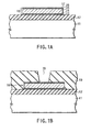
- FIGS. 1A through 1D are cross-sectional views in the order of steps of forming the first level and the second level of metal interconnections in accordance with an embodiment of the present invention.
- the semiconductor device manufacturing method of the invention uses conventional sputtering equipment and its sputtering process is implemented by more than one step to deposit thin films made of metal within the same chamber while controlling three important parameters: the in-chamber pressure, the flow rate of a backside Ar gas, and the sputtering power.
- the wafer temperature is controlled by turning the backside Ar gas on or off and the deposition rate is controlled by changing the sputtering power.
- an Al-Cu film of several hundreds of nm in thickness is deposited at a low temperature below 150°C and a low sputtering power with the backside Ar gas turned off.
- the wafer is heated at a heater temperature of 350°C with the backside Ar gas supplied and an Al-Cu film is then deposited at a high deposition rate based on a high sputtering power.
- a heater temperature of 350°C with the backside Ar gas supplied and an Al-Cu film is then deposited at a high deposition rate based on a high sputtering power.
- two types of metal thin films consisting of low- and high-temperature metal particles are formed in sequence.
- the low-temperature, low-sputtering-power process provides good coverage in via holes but requires a long deposition time.
- the high-temperature, high-sputtering-power process can reduce the deposition time but provides poor coverage in the via holes.
- the two processes are used in combination.
- the low-temperature low-sputtering-power process is first carried out to fill in part of the via hole and the high-temperature high-sputtering-power process is then performed to form a metal thin film, thereby ensuring good coverage in the via holes and reducing the deposition time.
- the Al-Cu deposition chamber in the conventional sputtering equipment can be used to satisfy the 256-Mb DRAM requirement of having small via holes filled in and ensure sufficient reliability.
- high-quality BEOL wiring can be formed without sacrificing productivity and manufacturing cost.
- FIGS. 1A through 1D illustrate steps of manufacture of a semiconductor device in accordance with the present invention, particularly steps of forming the first and second levels of interconnects.
- a Ti film 13, a TiN film 14, an Al-Cu film 15, a Ti film 16 and a TiN film 17 are formed in sequence onto an insulating layer 12 formed over a surface of a semiconductor substrate 11.
- those films are patterned to form a first layer (M1) 18 of metal interconnect.
- the Ti film 13, the TiN film 14, the Al-Cu film 15, the Ti film 16 and the TiN film 17 are 10 nm, 10 nm, 230 nm, 5 nm, and 40 nm, respectively, in thickness.
- sinter annealing is carried out in a forming gas at 400°C for 20 minutes.
- an interlayer insulating film 19 of 600 nm in thickness is formed on the first metal interconnect layer 18 and the insulating film 12 and an opening (via hole) 20 is then formed in the interlayer insulating film 19 by means of lithographic and RIE techniques.
- a second metal interconnect layer (M2) 21 is formed on the interlayer insulating film 19 and in the via hole 20.
- a Ti film 22 of 25 nm in thickness and a TiN film 23 of 25 nm in thickness are first formed in sequence in a Ti/TiN sputtering chamber and then, in an Al sputtering chamber having its heater temperature set at 150°C, Al-Cu is sputtered for 55 seconds at a low sputtering power of 3.2 kW with no flow of wafer backside heating Ar gas.
- an Al-Cu film 24-1 of 300 nm in thickness was formed at a low temperature (which may be 50°C or room temperature much lower than 150°C).
- the wafer temperature will be below 150°C because the thermal conductivity between the heater and the wafer is poor, leading to a similar result.
- the time required to raise the heater temperature is further reduced.
- the heating Ar gas is introduced for 45 seconds to heat the wafer up to 350°C.
- Al-Cu is then sputtered at a high sputtering power of 12.7 kW for 32 seconds with heating Ar gas flow.
- an Al-Cu film 24-2 of 700 nm is formed at high temperature.
- an Al-Cu film 24 having a total thickness of 1 ⁇ m is formed.
- a TiN film 25 is formed at a thickness of 37.5 nm in the Ti/TiN sputtering chamber.
- the second metal interconnect layer 21 is patterned by means of lithography and RIE techniques, thereby completing the multilevel wiring process.
- the via hole 20 is filled in by the Al-Cu film 24-1 formed at low temperature to provide good coverage and then the Al-Cu film 24-2 is formed at high temperature to provide high deposition yield. Therefore, the second metal interconnect layer 21 can be formed in a short time while suppressing the formation of a void in the via hole 20. Thus, the problems encountered in using the long throw sputtering or the collimated sputtering can be eliminated, ensuring high throughput and low cost.
- the long throw sputtering and the collimated sputtering require six to seven minutes to form a metal interconnect layer of 1 ⁇ m in thickness, while the above-described inventive method can form a metal interconnect layer of the same thickness in less than three minutes, significantly improving the throughput.
- the inventive method does not suffer from an increase in cost due to consumable parts and down time due to consumable part replacement. From these points of view as well, the inventive method can reduce cost and improve throughput.
- the inventors formed via contact between first and second levels of interconnects for 256-Mb DRAM BEOL wiring in accordance with various manufacturing methods and performed stress tests.
- the second level of interconnect consists of a Ti film of 25 nm in thickness, a TiN film of 25 nm in thickness, an Al-Cu film of 1 ⁇ m in thickness, and a TiN film of 37.5 nm in thickness which were stacked in the order mentioned.
- the Al-Cu film was formed in accordance with the following methods:
- a chip is defined to be defective when it shows an increase of 20% in contact resistance under conditions of a test temperature of 245°C and a current flow of 11.00 mA between the first and second levels of interconnects. Then, early failures (which occur within five hours from the start of testing) were observed on six chips of 50 chips for the via contact made in accordance with the method (a). No early failures were observed on 50 chips manufactured in the accordance with each of the methods (b), (c), and (d). The method (b) is less than three minutes in the required process time, while the methods (c) and (d) each need six to seven minutes because the Al-Cu film deposition rate is low.
- the cost of manufacturing a semiconductor device in accordance with the present invention is reduced drastically by reducing the process time.
- the cost of consumable parts can also be reduced because there is no need of collimator replacement and moreover the frequency of target replacement is low.
- the embodiment of the present invention has been described in terms of an example of turning the backside Ar gas on and off in the sputtering equipment to change the conductivity of heat generated by the heater. This is not restrictive.
- the thermal conductivity between the heater and the wafer may likewise be changed by turning the electrostatic chuck of the sputtering equipment on and off.
- the above-described embodiment has been described as first depositing the Al-Cu film 24-1 of 300 nm in thickness at low temperature and low sputtering power and then depositing the Al-Cu film 24-2 of 700 nm in thickness at higher temperature and higher sputtering power.
- the thickness of the Al-Cu film formed at low temperature and low sputtering power may be in a range from 300 to 700 nm, and the Al-Cu film deposited at high temperature and high sputtering power may be in a range from 700 to 300 nm. If the thickness of the Al-Cu film deposited at low temperature and low sputtering power were less than 300 nm, then the void suppressing effect would be lessened. If, on the other hand, the thickness were greater than 700 nm, the sputtering time would increase. Thus, it is required to determine the thickness of each Al-Cu film and the sputtering power taking into account the size and depth of the via hole, the required coverage in the via hole, and the manufacturing time.
- a semiconductor device manufacturing method which can improve throughput and reduce manufacturing cost while suppressing the formation of voids.
Landscapes
- Chemical & Material Sciences (AREA)
- Chemical Kinetics & Catalysis (AREA)
- Engineering & Computer Science (AREA)
- Materials Engineering (AREA)
- Mechanical Engineering (AREA)
- Metallurgy (AREA)
- Organic Chemistry (AREA)
- Internal Circuitry In Semiconductor Integrated Circuit Devices (AREA)
- Electrodes Of Semiconductors (AREA)
Claims (14)
- Procédé de fabrication d'un dispositif à semiconducteurs comprenant :a) un premier stade de formation d'une pellicule (12) isolante sur une surface d'un substrat (11) semi-conducteur ;b) un deuxième stade de formation d'une ouverture (20) dans la pellicule (12) isolante ;c) un troisième stade de formation d'une première couche (18) de métal en utilisant une matière métallique contenant au moins l'un de l'aluminium et du cuivre comme constituant principal sur la pellicule isolante et dans l'ouverture (20) à une première vitesse de dépôt, à une première température de tranche inférieure à 150°C et à une première puissance de pulvérisation cathodique, le substrat (11) semi-conducteur étant placé dans une chambre unique d'un équipement de pulvérisation cathodique ; etd) un quatrième stade de formation d'une deuxième couche (21) de métal en utilisant la matière contenant au moins l'un de l'aluminium ou du cuivre comme constituant principal sur la première couche de métal directement après le troisième stade à une deuxième vitesse de dépôt supérieure à la première vitesse de dépôt, à une deuxième température de tranche supérieure à la première température et dans une plage allant de 300°C à 400°C et à une deuxième puissance de pulvérisation cathodique supérieure à la première puissance de pulvérisation cathodique dans ladite chambre de l'équipement de pulvérisation cathodique.
- Procédé suivant la revendication 1, dans lequel la deuxième puissance de pulvérisation cathodique est environ quatre fois plus grande que la première puissance de pulvérisation cathodique.
- Procédé suivant la revendication 1, dans lequel on produit une différence entre la première température et la deuxième température en changeant la conductivité thermique entre la tranche et un dispositif de chauffage prévu dans la chambre de l'équipement de pulvérisation cathodique.
- Procédé suivant la revendication 3, dans lequel on change la conductivité thermique entre la tranche et le dispositif de chauffage en interrompant l'arrivée d'argon gazeux du côté arrière dans l'équipement de pulvérisation cathodique pendant le troisième stade et en faisant arriver de l'argon gazeux du côté arrière pendant le quatrième stade.
- Procédé suivant la revendication 3, dans lequel la tranche est portée par une mâchoire électrostatique et dans lequel on change la conductivité thermique entre la tranche et le dispositif de chauffage en mettant hors circuit une mâchoire électrostatique de l'équipement de pulvérisation cathodique pendant le troisième stade et en mettant en circuit la mâchoire électrostatique pendant le quatrième stade.
- Procédé suivant la revendication 1 comprenant, en outre, un cinquième stade de formation d'une première couche métallique de barrière entre le deuxième et le troisième stade et un sixième stade de formation d'une deuxième couche métallique de barrière sur la deuxième couche de métal à la suite du quatrième stade.
- Procédé suivant la revendication 6 comprenant, en outre, un septième stade de formation d'une couche d'interconnexion au-dessus du substrat semi-conducteur avant le premier stade et dans lequel on forme la pellicule isolante de la couche d'interconnexion et on forme l'ouverture (20) en ce qu'une partie de la pellicule isolante est disposée au-dessus de la couche d'interconnexion.
- Procédé suivant la revendication 7, dans lequel le septième stade comprend un stade de formation d'une troisième couche métallique de barrière sur le substrat semi-conducteur, un stade de formation d'une troisième couche métallique sur la troisième couche métallique de barrière, un stade de formation d'une quatrième couche métallique de barrière sur la troisième couche métallique de barrière et un stade de structuration de la troisième couche métallique de barrière, de la troisième couche métallique et de la quatrième couche métallique de barrière.
- Procédé suivant la revendication 8 comprenant, en outre, un stade de formation d'une cinquième couche métallique de barrière dans l'ouverture entre la quatrième couche métallique de barrière et la première couche métallique de barrière.
- Procédé suivant la revendication 9, dans lequel chacune des première à cinquième couches métalliques de barrière contient un métal réfractaire.
- Procédé suivant la revendication 8, dans lequel chacune des première à quatrième couches métalliques de barrière contient du nitrure de titane.
- Procédé suivant la revendication 8, dans lequel chacune des première à quatrième couches métalliques de barrière contient des couches empilées de titane et de nitrure de titane.
- Procédé suivant la revendication 9, dans lequel la cinquième couche métallique de barrière contient du titane.
- Procédé suivant l'une des revendications précédentes, dans lequel, dans le quatrième stade, la deuxième couche de métal est formée de manière contiguë à la première couche de métal en utilisant la matière contenant au moins l'un de l'aluminium et du cuivre comme constituant principal.
Applications Claiming Priority (2)
| Application Number | Priority Date | Filing Date | Title |
|---|---|---|---|
| US63094 | 1993-05-14 | ||
| US09/063,094 US6140236A (en) | 1998-04-21 | 1998-04-21 | High throughput A1-Cu thin film sputtering process on small contact via for manufacturable beol wiring |
Publications (3)
| Publication Number | Publication Date |
|---|---|
| EP0954015A2 EP0954015A2 (fr) | 1999-11-03 |
| EP0954015A3 EP0954015A3 (fr) | 2002-09-11 |
| EP0954015B1 true EP0954015B1 (fr) | 2007-10-17 |
Family
ID=22046891
Family Applications (1)
| Application Number | Title | Priority Date | Filing Date |
|---|---|---|---|
| EP99107337A Expired - Lifetime EP0954015B1 (fr) | 1998-04-21 | 1999-04-21 | Procédé de pulvérisation cathodique de Al-Cu à haut débit sur un petit trou de contact |
Country Status (6)
| Country | Link |
|---|---|
| US (1) | US6140236A (fr) |
| EP (1) | EP0954015B1 (fr) |
| JP (1) | JP3335931B2 (fr) |
| KR (1) | KR100328901B1 (fr) |
| CN (1) | CN1155075C (fr) |
| DE (1) | DE69937317T2 (fr) |
Families Citing this family (29)
| Publication number | Priority date | Publication date | Assignee | Title |
|---|---|---|---|---|
| US6475912B1 (en) * | 1998-06-01 | 2002-11-05 | Matsushita Electric Industrial Co., Ltd. | Semiconductor device and method and apparatus for fabricating the same while minimizing operating failures and optimizing yield |
| JP3892609B2 (ja) * | 1999-02-16 | 2007-03-14 | 株式会社東芝 | ホットプレートおよび半導体装置の製造方法 |
| US6627542B1 (en) * | 1999-07-12 | 2003-09-30 | Applied Materials, Inc. | Continuous, non-agglomerated adhesion of a seed layer to a barrier layer |
| JP4163331B2 (ja) * | 1999-07-14 | 2008-10-08 | アルバック成膜株式会社 | 位相シフタ膜の製造方法、位相シフトマスク用ブランクスの製造方法、および、位相シフトマスクの製造方法 |
| US6413863B1 (en) * | 2000-01-24 | 2002-07-02 | Taiwan Semiconductor Manufacturing Company | Method to resolve the passivation surface roughness during formation of the AlCu pad for the copper process |
| US6613671B1 (en) * | 2000-03-03 | 2003-09-02 | Micron Technology, Inc. | Conductive connection forming methods, oxidation reducing methods, and integrated circuits formed thereby |
| KR100477812B1 (ko) * | 2000-07-31 | 2005-03-21 | 주식회사 하이닉스반도체 | 구리를 사용한 금속 콘택 형성방법 |
| US6373135B1 (en) * | 2000-09-14 | 2002-04-16 | Infineon Technologies Ag | Semiconductor structure and method of fabrication |
| US6635564B1 (en) * | 2000-09-14 | 2003-10-21 | Infineon Technologies Ag | Semiconductor structure and method of fabrication including forming aluminum columns |
| KR100368984B1 (ko) * | 2001-01-10 | 2003-01-24 | 주식회사 하이닉스반도체 | 반도체 장치의 금속층 형성조건 제어방법 |
| JP2003318395A (ja) * | 2002-04-19 | 2003-11-07 | Hitachi Ltd | 半導体装置の製造方法 |
| US7138719B2 (en) * | 2002-08-29 | 2006-11-21 | Micron Technology, Inc. | Trench interconnect structure and formation method |
| JP4936643B2 (ja) * | 2004-03-02 | 2012-05-23 | 株式会社リコー | 半導体装置及びその製造方法 |
| JP4501533B2 (ja) * | 2004-05-31 | 2010-07-14 | 株式会社デンソー | 半導体装置の製造方法 |
| JP2007027234A (ja) * | 2005-07-13 | 2007-02-01 | Seiko Epson Corp | 半導体装置及びその製造方法 |
| US20070138001A1 (en) * | 2005-12-19 | 2007-06-21 | Teng-Yuan Ko | Method of forming an inductor on a semiconductor substrate |
| TWI278265B (en) * | 2006-01-09 | 2007-04-01 | Phoenix Prec Technology Corp | Method for fabricating circuit board with electrically conducting structure and the same |
| JP4833014B2 (ja) * | 2006-10-02 | 2011-12-07 | キヤノンアネルバ株式会社 | 高温リフロースパッタリング装置 |
| KR100875822B1 (ko) * | 2007-07-12 | 2008-12-26 | 주식회사 동부하이텍 | 반도체 장치 형성 방법 |
| US20090050471A1 (en) * | 2007-08-24 | 2009-02-26 | Spansion Llc | Process of forming an electronic device including depositing layers within openings |
| JP2009164510A (ja) * | 2008-01-10 | 2009-07-23 | Renesas Technology Corp | 半導体装置および半導体装置の製造方法 |
| CN105990227B (zh) * | 2015-02-27 | 2019-11-08 | 中芯国际集成电路制造(上海)有限公司 | 金属连线的制作方法及半导体器件 |
| CN104934332A (zh) * | 2015-04-29 | 2015-09-23 | 安徽松泰包装材料有限公司 | 一种铜铝复合薄膜生产工艺 |
| US10586732B2 (en) | 2016-06-30 | 2020-03-10 | International Business Machines Corporation | Via cleaning to reduce resistance |
| US10707152B2 (en) * | 2017-01-16 | 2020-07-07 | Innolux Corporation | High-frequency device and manufacturing method thereof |
| CN110890318A (zh) * | 2018-09-11 | 2020-03-17 | 长鑫存储技术有限公司 | 接触孔填充方法及结构、集成电路芯片 |
| CN111304614B (zh) * | 2020-03-31 | 2022-03-08 | 宁波瑞凌新能源科技有限公司 | 反射膜、其制备方法及应用 |
| US12091752B2 (en) * | 2021-03-18 | 2024-09-17 | Taiwan Semiconductor Manufacturing Company, Ltd. | Apparatus and method of manufacturing interconnect structures |
| CN117127154B (zh) * | 2023-10-16 | 2024-08-06 | 粤芯半导体技术股份有限公司 | 一种半导体器件中的互连金属的沉积方法 |
Citations (2)
| Publication number | Priority date | Publication date | Assignee | Title |
|---|---|---|---|---|
| EP0493089A1 (fr) * | 1990-12-25 | 1992-07-01 | Ngk Insulators, Ltd. | Appareil de chauffage d'une tranche semi-conductrice et procédé pour sa fabrication |
| EP0360529B1 (fr) * | 1988-09-19 | 1997-06-04 | Toto Ltd. | Plateau de retenue électrostatique |
Family Cites Families (28)
| Publication number | Priority date | Publication date | Assignee | Title |
|---|---|---|---|---|
| US4495221A (en) * | 1982-10-26 | 1985-01-22 | Signetics Corporation | Variable rate semiconductor deposition process |
| KR900001825B1 (ko) * | 1984-11-14 | 1990-03-24 | 가부시끼가이샤 히다찌세이사꾸쇼 | 성막 지향성을 고려한 스퍼터링장치 |
| US4790920A (en) * | 1985-12-20 | 1988-12-13 | Intel Corporation | Method for depositing an al2 O3 cap layer on an integrated circuit substrate |
| US4721689A (en) * | 1986-08-28 | 1988-01-26 | International Business Machines Corporation | Method for simultaneously forming an interconnection level and via studs |
| US4910580A (en) * | 1987-08-27 | 1990-03-20 | Siemens Aktiengesellschaft | Method for manufacturing a low-impedance, planar metallization composed of aluminum or of an aluminum alloy |
| US4937657A (en) * | 1987-08-27 | 1990-06-26 | Signetics Corporation | Self-aligned metallization for semiconductor device and process using selectively deposited tungsten |
| FR2634317A1 (fr) * | 1988-07-12 | 1990-01-19 | Philips Nv | Procede pour fabriquer un dispositif semiconducteur ayant au moins un niveau de prise de contact a travers des ouvertures de contact de petites dimensions |
| US5071714A (en) * | 1989-04-17 | 1991-12-10 | International Business Machines Corporation | Multilayered intermetallic connection for semiconductor devices |
| US5658828A (en) * | 1989-11-30 | 1997-08-19 | Sgs-Thomson Microelectronics, Inc. | Method for forming an aluminum contact through an insulating layer |
| US5108570A (en) * | 1990-03-30 | 1992-04-28 | Applied Materials, Inc. | Multistep sputtering process for forming aluminum layer over stepped semiconductor wafer |
| US5173442A (en) * | 1990-07-23 | 1992-12-22 | Microelectronics And Computer Technology Corporation | Methods of forming channels and vias in insulating layers |
| JP2598335B2 (ja) * | 1990-08-28 | 1997-04-09 | 三菱電機株式会社 | 半導体集積回路装置の配線接続構造およびその製造方法 |
| KR960001601B1 (ko) * | 1992-01-23 | 1996-02-02 | 삼성전자주식회사 | 반도체 장치의 접촉구 매몰방법 및 구조 |
| US5345108A (en) * | 1991-02-26 | 1994-09-06 | Nec Corporation | Semiconductor device having multi-layer electrode wiring |
| US5523529A (en) * | 1991-03-26 | 1996-06-04 | Cable Ready, Inc. | Snap-fit protective molding assembly for electrical cables and entry tools therefor |
| US5175125A (en) * | 1991-04-03 | 1992-12-29 | Chartered Semiconductor Manufacturing Ltd. Pte | Method for making electrical contacts |
| TW520072U (en) * | 1991-07-08 | 2003-02-01 | Samsung Electronics Co Ltd | A semiconductor device having a multi-layer metal contact |
| US5231751A (en) * | 1991-10-29 | 1993-08-03 | International Business Machines Corporation | Process for thin film interconnect |
| US5262354A (en) * | 1992-02-26 | 1993-11-16 | International Business Machines Corporation | Refractory metal capped low resistivity metal conductor lines and vias |
| US5300813A (en) * | 1992-02-26 | 1994-04-05 | International Business Machines Corporation | Refractory metal capped low resistivity metal conductor lines and vias |
| US5371042A (en) * | 1992-06-16 | 1994-12-06 | Applied Materials, Inc. | Method of filling contacts in semiconductor devices |
| US5635763A (en) * | 1993-03-22 | 1997-06-03 | Sanyo Electric Co., Ltd. | Semiconductor device having cap-metal layer |
| US5366929A (en) * | 1993-05-28 | 1994-11-22 | Cypress Semiconductor Corp. | Method for making reliable selective via fills |
| US5527741A (en) * | 1994-10-11 | 1996-06-18 | Martin Marietta Corporation | Fabrication and structures of circuit modules with flexible interconnect layers |
| US5580823A (en) * | 1994-12-15 | 1996-12-03 | Motorola, Inc. | Process for fabricating a collimated metal layer and contact structure in a semiconductor device |
| JP3365112B2 (ja) * | 1994-12-16 | 2003-01-08 | ソニー株式会社 | 半導体装置の配線形成方法 |
| US5597458A (en) * | 1995-07-10 | 1997-01-28 | Advanced Micro Devices | Method for producing alloy films using cold sputter deposition process |
| EP0799903A3 (fr) * | 1996-04-05 | 1999-11-17 | Applied Materials, Inc. | Méthodes de pulvérisation d'un métal sur un substrat et dispositif de traitement de semiconducteurs |
-
1998
- 1998-04-21 US US09/063,094 patent/US6140236A/en not_active Expired - Lifetime
- 1998-10-27 JP JP30555398A patent/JP3335931B2/ja not_active Expired - Fee Related
-
1999
- 1999-04-21 EP EP99107337A patent/EP0954015B1/fr not_active Expired - Lifetime
- 1999-04-21 CN CNB991076214A patent/CN1155075C/zh not_active Expired - Fee Related
- 1999-04-21 KR KR1019990014181A patent/KR100328901B1/ko not_active Expired - Fee Related
- 1999-04-21 DE DE69937317T patent/DE69937317T2/de not_active Expired - Fee Related
Patent Citations (2)
| Publication number | Priority date | Publication date | Assignee | Title |
|---|---|---|---|---|
| EP0360529B1 (fr) * | 1988-09-19 | 1997-06-04 | Toto Ltd. | Plateau de retenue électrostatique |
| EP0493089A1 (fr) * | 1990-12-25 | 1992-07-01 | Ngk Insulators, Ltd. | Appareil de chauffage d'une tranche semi-conductrice et procédé pour sa fabrication |
Also Published As
| Publication number | Publication date |
|---|---|
| KR100328901B1 (ko) | 2002-03-14 |
| CN1155075C (zh) | 2004-06-23 |
| DE69937317D1 (de) | 2007-11-29 |
| EP0954015A3 (fr) | 2002-09-11 |
| JP3335931B2 (ja) | 2002-10-21 |
| EP0954015A2 (fr) | 1999-11-03 |
| DE69937317T2 (de) | 2008-07-03 |
| KR19990083367A (ko) | 1999-11-25 |
| CN1234606A (zh) | 1999-11-10 |
| JPH11307478A (ja) | 1999-11-05 |
| US6140236A (en) | 2000-10-31 |
Similar Documents
| Publication | Publication Date | Title |
|---|---|---|
| EP0954015B1 (fr) | Procédé de pulvérisation cathodique de Al-Cu à haut débit sur un petit trou de contact | |
| US5918149A (en) | Deposition of a conductor in a via hole or trench | |
| US5747360A (en) | Method of metalizing a semiconductor wafer | |
| US6482735B1 (en) | Method for improved metal fill by treatment of mobility layers | |
| US7297640B2 (en) | Method for reducing argon diffusion from high density plasma films | |
| EP1570517B1 (fr) | Procede pour deposer une couche de metal sur une structure d' interconnexion semi-conductrice possedant une couche de recouvrement | |
| US20040106279A1 (en) | Method and system for eliminating extrusions in semiconductor vias | |
| EP1313140A1 (fr) | Methode de formation d'une couche intermédiaire sous un bouchon de tungstène | |
| KR20010034151A (ko) | 금속화 방법 및 장치 | |
| US5582881A (en) | Process for deposition of a Ti/TiN cap layer on aluminum metallization and apparatus | |
| US6099701A (en) | AlCu electromigration (EM) resistance | |
| US6716733B2 (en) | CVD-PVD deposition process | |
| US6391778B1 (en) | Contact/via force fill techniques and resulting structures | |
| US6617231B1 (en) | Method for forming a metal extrusion free via | |
| US6949464B1 (en) | Contact/via force fill techniques | |
| CN100468691C (zh) | 凹槽的填充方法及其结构 | |
| HK1023448A (en) | High throughput al-cu thin film sputtering process on small contact via | |
| US6605531B1 (en) | Hole-filling technique using CVD aluminum and PVD aluminum integration | |
| US20070243708A1 (en) | Manufacturing method for an integrated semiconductor contact structure having an improved aluminum fill | |
| US6982226B1 (en) | Method of fabricating a contact with a post contact plug anneal | |
| US7189645B1 (en) | System and method for adjusting the ratio of deposition times to optimize via density and via fill in aluminum multilayer metallization | |
| KR20010026044A (ko) | 반도체 장치의 금속층 형성 방법 | |
| JP2000340565A (ja) | 半導体集積回路装置およびその製造方法 | |
| Helneder et al. | Novel AlCu: fill process for via applications | |
| KR19980083837A (ko) | 반도체장치의 콘택홀 매몰방법 |
Legal Events
| Date | Code | Title | Description |
|---|---|---|---|
| PUAI | Public reference made under article 153(3) epc to a published international application that has entered the european phase |
Free format text: ORIGINAL CODE: 0009012 |
|
| 17P | Request for examination filed |
Effective date: 19990421 |
|
| AK | Designated contracting states |
Kind code of ref document: A2 Designated state(s): AT BE CH CY DE DK ES FI FR GB GR IE IT LI LU MC NL PT SE |
|
| AX | Request for extension of the european patent |
Free format text: AL;LT;LV;MK;RO;SI |
|
| PUAL | Search report despatched |
Free format text: ORIGINAL CODE: 0009013 |
|
| AK | Designated contracting states |
Kind code of ref document: A3 Designated state(s): AT BE CH CY DE DK ES FI FR GB GR IE IT LI LU MC NL PT SE |
|
| AX | Request for extension of the european patent |
Free format text: AL;LT;LV;MK;RO;SI |
|
| 17Q | First examination report despatched |
Effective date: 20030102 |
|
| AKX | Designation fees paid |
Designated state(s): DE FR GB IE IT NL |
|
| RAP1 | Party data changed (applicant data changed or rights of an application transferred) |
Owner name: KABUSHIKI KAISHA TOSHIBA Owner name: INTERNATIONAL BUSINESS MACHINES CORPORATION Owner name: INFINEON TECHNOLOGIES AG |
|
| REG | Reference to a national code |
Ref country code: HK Ref legal event code: WD Ref document number: 1023448 Country of ref document: HK |
|
| GRAP | Despatch of communication of intention to grant a patent |
Free format text: ORIGINAL CODE: EPIDOSNIGR1 |
|
| GRAS | Grant fee paid |
Free format text: ORIGINAL CODE: EPIDOSNIGR3 |
|
| GRAA | (expected) grant |
Free format text: ORIGINAL CODE: 0009210 |
|
| AK | Designated contracting states |
Kind code of ref document: B1 Designated state(s): DE FR GB IE IT NL |
|
| REG | Reference to a national code |
Ref country code: GB Ref legal event code: FG4D |
|
| REG | Reference to a national code |
Ref country code: IE Ref legal event code: FG4D |
|
| REF | Corresponds to: |
Ref document number: 69937317 Country of ref document: DE Date of ref document: 20071129 Kind code of ref document: P |
|
| NLV1 | Nl: lapsed or annulled due to failure to fulfill the requirements of art. 29p and 29m of the patents act | ||
| PG25 | Lapsed in a contracting state [announced via postgrant information from national office to epo] |
Ref country code: NL Free format text: LAPSE BECAUSE OF FAILURE TO SUBMIT A TRANSLATION OF THE DESCRIPTION OR TO PAY THE FEE WITHIN THE PRESCRIBED TIME-LIMIT Effective date: 20071017 |
|
| EN | Fr: translation not filed | ||
| PLBE | No opposition filed within time limit |
Free format text: ORIGINAL CODE: 0009261 |
|
| STAA | Information on the status of an ep patent application or granted ep patent |
Free format text: STATUS: NO OPPOSITION FILED WITHIN TIME LIMIT |
|
| 26N | No opposition filed |
Effective date: 20080718 |
|
| PG25 | Lapsed in a contracting state [announced via postgrant information from national office to epo] |
Ref country code: FR Free format text: LAPSE BECAUSE OF FAILURE TO SUBMIT A TRANSLATION OF THE DESCRIPTION OR TO PAY THE FEE WITHIN THE PRESCRIBED TIME-LIMIT Effective date: 20080801 |
|
| GBPC | Gb: european patent ceased through non-payment of renewal fee |
Effective date: 20080421 |
|
| PG25 | Lapsed in a contracting state [announced via postgrant information from national office to epo] |
Ref country code: IE Free format text: LAPSE BECAUSE OF NON-PAYMENT OF DUE FEES Effective date: 20080421 |
|
| PG25 | Lapsed in a contracting state [announced via postgrant information from national office to epo] |
Ref country code: GB Free format text: LAPSE BECAUSE OF NON-PAYMENT OF DUE FEES Effective date: 20080421 |
|
| PGFP | Annual fee paid to national office [announced via postgrant information from national office to epo] |
Ref country code: DE Payment date: 20090625 Year of fee payment: 11 |
|
| PG25 | Lapsed in a contracting state [announced via postgrant information from national office to epo] |
Ref country code: IT Free format text: LAPSE BECAUSE OF NON-PAYMENT OF DUE FEES Effective date: 20080430 Ref country code: DE Free format text: LAPSE BECAUSE OF NON-PAYMENT OF DUE FEES Effective date: 20101103 |