EP0954823B1 - Verstärker mit variabler verstärkung und optisches sensorsystem für eine geldscheingültigkeitskontrolle - Google Patents
Verstärker mit variabler verstärkung und optisches sensorsystem für eine geldscheingültigkeitskontrolle Download PDFInfo
- Publication number
- EP0954823B1 EP0954823B1 EP98951988A EP98951988A EP0954823B1 EP 0954823 B1 EP0954823 B1 EP 0954823B1 EP 98951988 A EP98951988 A EP 98951988A EP 98951988 A EP98951988 A EP 98951988A EP 0954823 B1 EP0954823 B1 EP 0954823B1
- Authority
- EP
- European Patent Office
- Prior art keywords
- microcontroller
- variable gain
- amplifier circuit
- gain amplifier
- optical sensor
- Prior art date
- Legal status (The legal status is an assumption and is not a legal conclusion. Google has not performed a legal analysis and makes no representation as to the accuracy of the status listed.)
- Expired - Lifetime
Links
- 230000003287 optical effect Effects 0.000 title claims description 37
- 230000009977 dual effect Effects 0.000 claims description 8
- 238000010586 diagram Methods 0.000 description 10
- 238000005259 measurement Methods 0.000 description 9
- 238000000034 method Methods 0.000 description 4
- 238000012545 processing Methods 0.000 description 4
- 238000012544 monitoring process Methods 0.000 description 3
- 230000005540 biological transmission Effects 0.000 description 2
- 238000004519 manufacturing process Methods 0.000 description 2
- 229920003023 plastic Polymers 0.000 description 2
- 238000010200 validation analysis Methods 0.000 description 2
- 230000002411 adverse Effects 0.000 description 1
- 230000032683 aging Effects 0.000 description 1
- 238000006243 chemical reaction Methods 0.000 description 1
- 230000003749 cleanliness Effects 0.000 description 1
- 238000013480 data collection Methods 0.000 description 1
- 238000013461 design Methods 0.000 description 1
- 238000009792 diffusion process Methods 0.000 description 1
- 238000009826 distribution Methods 0.000 description 1
- 230000006870 function Effects 0.000 description 1
- 238000003780 insertion Methods 0.000 description 1
- 230000037431 insertion Effects 0.000 description 1
- 239000000463 material Substances 0.000 description 1
- 238000012986 modification Methods 0.000 description 1
- 230000004048 modification Effects 0.000 description 1
- 230000008569 process Effects 0.000 description 1
- 230000004044 response Effects 0.000 description 1
- 230000002441 reversible effect Effects 0.000 description 1
- 239000004065 semiconductor Substances 0.000 description 1
- 230000035945 sensitivity Effects 0.000 description 1
- 238000003860 storage Methods 0.000 description 1
- 238000012360 testing method Methods 0.000 description 1
Images


Classifications
-
- H—ELECTRICITY
- H03—ELECTRONIC CIRCUITRY
- H03G—CONTROL OF AMPLIFICATION
- H03G3/00—Gain control in amplifiers or frequency changers
- H03G3/20—Automatic control
- H03G3/30—Automatic control in amplifiers having semiconductor devices
- H03G3/3084—Automatic control in amplifiers having semiconductor devices in receivers or transmitters for electromagnetic waves other than radiowaves, e.g. lightwaves
-
- G—PHYSICS
- G07—CHECKING-DEVICES
- G07D—HANDLING OF COINS OR VALUABLE PAPERS, e.g. TESTING, SORTING BY DENOMINATIONS, COUNTING, DISPENSING, CHANGING OR DEPOSITING
- G07D7/00—Testing specially adapted to determine the identity or genuineness of valuable papers or for segregating those which are unacceptable, e.g. banknotes that are alien to a currency
- G07D7/06—Testing specially adapted to determine the identity or genuineness of valuable papers or for segregating those which are unacceptable, e.g. banknotes that are alien to a currency using wave or particle radiation
- G07D7/12—Visible light, infrared or ultraviolet radiation
- G07D7/121—Apparatus characterised by sensor details
-
- H—ELECTRICITY
- H03—ELECTRONIC CIRCUITRY
- H03G—CONTROL OF AMPLIFICATION
- H03G1/00—Details of arrangements for controlling amplification
- H03G1/0005—Circuits characterised by the type of controlling devices operated by a controlling current or voltage signal
- H03G1/0017—Circuits characterised by the type of controlling devices operated by a controlling current or voltage signal the device being at least one of the amplifying solid-state elements
- H03G1/0023—Circuits characterised by the type of controlling devices operated by a controlling current or voltage signal the device being at least one of the amplifying solid-state elements in emitter-coupled or cascode amplifiers
Definitions
- the present invention pertains to a device and technique for providing a stable optical sensor system.
- the invention concerns a variable gain amplifier circuit for controlling leakage current in an optical sensor system of a bill validator, and a method for obtaining light measurements.
- Bill validators used in vending machines and the like typically utilize optical, magnetic and other sensors to obtain measurements from an inserted bill to determine authenticity and denomination.
- the bill is transported past a plurality of photosensors, typically made up of light-emitting diodes (LEDs) and phototransistors, and a plurality of signals are generated corresponding to measurements taken from different areas of the bill.
- the LED drive signals are typically multiplexed between two or more LEDs to emit light at a number of wavelengths in a short period of time to ensure high security against fraud. The signals are then processed to validate and authenticate the bill.
- the output power of an LED can degrade on the order of fifty percent with aging, inserted bills are of differing quality, and bill path cleanliness may vary. Further, some bill validator applications require undiminished performance under harsh outdoor conditions such as extreme cold or heat, and such temperature changes can cause wildly varying gain characteristics in LED-receiver pairs resulting in erroneous sensor readings. In addition, there are normal production variations in LED optical power output and receiver sensitivity, which can lead to units having varying current and voltage requirements in order to operate effectively. In order to compensate for such phenomena, optical sensor measurements were taken over a large dynamic range.
- U.S. Pat. No. 5,682,119 provides a variable gain circuit which includes a pair of input signals of opposite polarities are connected to differential inputs of two differential amplifiers. A control signal is connected to a third differential amplifier which is connected to first and second current sources by means of a voltage to current conversion circuit.
- Embodiments of the invention feature an improved optical sensor system for use in a currency validator.
- the optical sensor system includes a microcontroller, a plurality of light transmitters, a plurality of light receivers for producing signals, and a variable gain amplifier circuit connected to the receivers and to the microcontroller.
- the microcontroller controls the gain of the variable gain amplifier based on predetermined measurements of each light transmitter, and the variable gain amplifier includes dual transconductance amplifiers having an input signal applied to a bias current input and having their differential inputs inversely connected together to compensate for leakage current over a wide range of temperatures.
- the optical sensor system may also include one or more of the following features.
- a twelve-bit digital-to-analog converter may be connected between the microcontroller and the plurality of light transmitters.
- a memory connected to the microcontroller may be included for storing predetermined light transmitter and receiver circuit values. At least one of the light transmitters may be an optical package containing at least two LEDs, wherein each LED transmits light of a different wavelength.
- a twelve-bit analog-to-digital converter may be connected between the variable gain amplifier and the microcontroller, a gain analog-to-digital converter may be connected between the microcontroller and the variable gain amplifier, and a multiplexer may be connected between the receivers and the variable gain amplifier, and having an input connected to the microcontroller.
- a motor drive circuit may be included for controlling a transport motor and a stacker motor.
- Embodiments of the invention also concern, generally, a variable gain amplifier circuit.
- An operational transconductance amplifier circuit has dual transconductance amplifiers having an input signal applied to a bias current input, and having their differential inputs inversely connected together.
- variable gain amplifier circuit may also include one or more of the following features.
- a transconductance amplifier circuit for converting a voltage signal into a current signal output, wherein the output may be connected to the bias current input of the dual transconductance amplifiers.
- a variable transistor may be connected to the transconductance amplifier circuit for selecting the transconductance.
- An overcurrent protection circuit may be connected between the transconductance amplifier and the operational transconductance amplifier circuit.
- a bill validator includes a variable gain amplifier with a continually adjustable gain driven by a twelve-bit gain DAC.
- a microprocessor uses a twelve-bit LED DAC for making LED current adjustments.
- the enhanced adjustability provided by this circuitry ensures adequate signal levels for reliable LED and receiver pair operation over the validator's lifetime.
- such a design permits using LED components with a wider distribution of characteristics, thus avoiding a costly sorting process during manufacturing to find LEDs that are within acceptable tolerance levels.
- Embodiments of the invention also provide low offsets across an extended temperature range through the use of leakage current compensation in the transconductance amplifiers of the variable gain amplifier circuitry. The result is consistent performance and security across the product's usable temperature range.
- embodiments of the invention provide a stable, variable gain amplifier for use with an optical sensor system.
- the variable gain amplifier amplifies low level, medium bandwidth sensor signals at a continuously variable range of gains while maintaining low offsets over a wide temperature range.
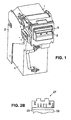
- Fig. 1 is a perspective view of a currency validator and transport unit 1 connected to a bill stacker 2 and currency container or cashbox 4.
- currency used herein means any paper currency, bill, banknote or other security document which may be used to pay for goods or services.
- the bill validator and transport unit may have a bezel 6 designed to fit through an aperture in the front panel of a vending machine, gaming machine such as a slot machine, and the like.
- a bill entryway 8 is incorporated in the bezel for the insertion of currency.
- Fig. 2A is an enlarged side view of the interior of the bill validator and transport system 1.
- the bill entryway 8 leads to a bill passageway 9.
- the beginning of the bill passageway is defined by an upper housing 5 and a lower housing 7.
- Disposed on the bottom of the bill passageway is a set of continuous belts 10 (one on each side of the bill passageway) which fit through openings (not shown) in the lower housing 7 to contact a bill.
- the belts 10 are connected to a drive wheel 12, a pulley wheel 14 and various other tensioning wheels 16.
- a reversible transport motor 18 is connected via a series of gears (not shown) to the drive wheels 12.
- Pulley wheels 20, 22 are located on the top of the bill passageway which fit through openings in the upper housing 5 and are opposite the drive wheel and pulley wheel 14.
- a pair of continuous transport belts 24 are connected to tensioning wheels 26 on the top of the bill passageway.
- a banknote When a banknote is inserted into the currency validator and transport unit 1, one or more sensors cause the transport motor 18 to start.
- the bill is gripped between the belts 10 and wheels 20 and advanced through the bill passageway 9 (from left to right in Fig. 2A) to encounter a plurality of optical and other sensors. If the information gathered by the sensors at any given point indicates that the bill is not genuine, then the transport motor 18 is reversed and the bill is rejected. Data collection continues until an escrow sensor (not shown) indicates that the bill transport should be stopped, at which time a braking signal is applied to the motor. The banknote is then validated and denominated, and the vending machine checked to see if the proper merchandise is available.
- a currency validator contains a plurality of optical sensors located along the bill passageway 9 to generate electrical signals in response to features of a bill.
- Fig. 2B is a simplified top view diagram 27 of the positions of the LEDs of the front optical sensors in the embodiment of Fig. 2A.
- These front optical sensors are comprised of transmitters (for example, light emitting diodes or LEDs) and receivers (such as phototransistors) positioned in the upper housing 5 and lower housing 7 on opposite sides of the bill passageway 9 near the bill entryway 8.
- a bill 29 would be inserted in the direction of arrow 28 to be transported between the front optical sensors.
- An optical escrow sensor (not shown) is also used to sense when the trailing edge of a bill has passed, and may be located in a position in the upper and lower housings in between the pulley wheels 20 and 22 (see Fig. 2A).
- the optical sensors used in the validator apparatus are encased in the upper and lower housings to prevent dirt and other foreign matter from adhering to the sensors, and to prevent tampering.
- at least one front optical sensor transmits and receives infra-red wavelength signals. Consequently, the upper and lower housings are preferably made of transparent plastic, in particular a red transparent plastic material having optical characteristics which permit the unobstructed transmission of infra-red waves.
- Fig. 3 is a simplified validator block diagram 30.
- a microcontroller 32 is connected to an EEPROM 34, which stores predetermined values for use when processing signals from each of the optical transmitters (LEDs).
- the microcontroller performs all processing of signals to validate and denominate an inserted banknote, and transmits information such as credit data, hardware error messages, in-service and out-of-service messages and the like to the host system through host interface 36.
- the microcontroller controls each LED in the LED circuitry 38 through latch 37, and provides drive current through LED digital-to-analog converter (DAC) 40.
- DAC digital-to-analog converter
- a corresponding receiver When an LED is selected and energized, a corresponding receiver (one of the phototransistors in the receiver circuitry 42) generates a signal which is received by the microcontroller through multiplexer 44, variable gain amplifier 46, and a twelve-bit receiver analog-to-digital converter (ADC) 48.
- the microcontroller also controls the gain of the variable gain amplifier 46 through gain digital to analog converter (DAC) 50 for the particular receiver.
- DAC digital to analog converter
- the microcontroller selects the receiver of interest by specifying an address through latch 52 to multiplexer 44.
- the microcontroller 32 is also connected to the transport motor 18 and stacker motor 56 through a latch 53 and a motor drive circuit 54.
- the transport motor has an associated tachometer 57 for accurately monitoring the position of a banknote in the banknote passageway 9, and the stacker motor has an associated stacker home sensor 58 for monitoring the home position of the bill stacker.
- the escrow sensor, tachometer 57 and stacker home sensor 58 provide accurate information regarding bill position in the device.
- the LED DAC 40 and gain DAC 50 are preset to appropriate settings during calibration of the bill validator optical sensors. Calibration occurs when the validator is placed in calibration mode and white paper having transmissivity and diffusion characteristics similar to a banknote is inserted.
- the validator sets the gain DAC to an arbitrary number (for example, 1400 out of a full scale of 4095), and adjusts the LED DAC setting for each LED until the ADC 48 reading for that LED is equal to the arbitrary number (e.g. 1400).
- the setting value of the LED DAC for each LED can then be permanently stored in EEPROM 34, so that any time a given LED is turned ON its corresponding LED DAC setting is recalled and used. Alternately, the settings for the LED DAC and gain DAC can be calculated as the bill validator is used by the microcontroller.
- the microcontroller 32 directs transport drive motor 18 to drive the banknote between the LED circuits 38 and receivers 42 to obtain measurements of the light transmitted through the banknote.
- measurements of the light transmission characteristics of the banknote are utilized to authenticate the bill, and these bill validation measurements are taken until the bill clears the front optical sensors.
- Fig. 4A is a simplified circuit diagram of an embodiment of the LED circuitry 38.
- the cross channel (CC) LED 60 the start right (SR) LED 61, the start left (SL) LED 62, and recognition LED group one 64 and recognition LED group two 65.
- the recognition LED groups may contain two or more LEDs, wherein each LED in a recognition group may be of a different wavelength than the other LED(s) in that group.
- one LED in the recognition group 64 and one LED in recognition group 65 may transmit light of Xnm wavelength, while another LED in each may transmit light of Ynm wavelength.
- a third wavelength light of Znm could also be present.
- the microcontroller selects which LEDs to turn ON in which recognition unit via the select lines A, B and C respectively labelled 67, 68 and 69.
- Fig. 4B is a circuit diagram of the receiver circuitry 42 of Fig. 3 connected to a multiplexer 44. As shown, an escrow position phototransistor 80, a left start phototransistor 81, a right start phototransistor 82 and a cross-channel phototransistor are connected directly to the multiplexer 44. Also connected to the multiplexer through amplifier circuitry are recognition receivers A, B, C and D, or phototransistors 84, 85, 86 and 87, respectively. The microcontroller 32 selects the appropriate receiver or phototransistor by sending the select signals on select lines 67, 68 and 69. The output of the multiplexer 44 is then sent to the variable gain amplifier 46.
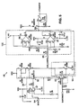
- Fig. 5 is a circuit diagram of the variable gain amplifier 46 of Fig. 3.
- a transconductance amplifier 90 is comprised of an operational amplifier 91, transistors 92 and 93 and resistors R1, R2 and R3.
- the transconductance amplifier 90 has a gain proportional to the input signal on line 94, and takes the input voltage from one of the receiver phototransistors chosen in multiplexer 44 and converts it to a current flowing into the collector of transistor 92.
- the transconductance of this stage is selectable via transistor 93 and the values of R2 and R3 to either 303 uA/V or 13.6 uA/V.
- R1 serves to limit the maximum current flowing through the transistor 92.
- the current in transistor 92 is mirrored by transistors Q2-Q4 so that the current flowing out of the collector of Q4 is roughly equal to the current flowing into the collector of the transistor 92.
- the combination of Q6 and R4 form an overcurrent protect circuit 95 for the bias current input (pin 1) of U2A.
- An operational transconductance amplifier circuit 100 is formed of dual transconductance amplifiers U2A 96 and U2B 97, and functions as a variable gain block. The gain is controlled by a 0-4 volt signal applied at the gain control input line 98 at resistor R6.
- the operational transconductance amplifier comprising amplifiers 96 and 97 (such as an LM13600 manufactured by National Semiconductor of California) has linearizing diodes that are used to convert the voltage across R6 into a linear bias for the differential inputs of U2A 96 and U2B 97.
- the input signal is fed (as a current) into the bias current input (pin 1) of U2A.
- This input is conventionally used as a gain control input in operational transconductance amplifiers, with the amplified signal fed to the differential inputs.
- the input signal to the bias current input much lower offsets are achieved, with the prime source of offsets being leakage currents in the current mirror at the bias current input rather than poor transistor matching in the input differential pair.
- the maximum bias current leakage specification for the LM13600 is 100 nA at a temperature of 25°C, which would result in a 10 mV offset across resistor R9. This offset increases by about a decade for every 40°C, so if the transconductance amplifiers U2A and U2B (96 and 97) were connected in a conventional manner, at a temperature of 65°C the offset could grow to an objectionable 100 mV.
- the differential inputs of U2B 96 are inversely connected to the differential inputs of U2A 97 as shown in Fig. 5, such that the gain of U2B is -1 times the gain of U2A.
- the bias current input of U2B is connected to a -5V source, so that the only current flowing into the output (pin 12) is due to leakage current.
- This output pin is tied to the output of U2A (pin 5) such that the leakage current contribution of the signal current flowing out of pin 5 is compensated by the leakage current signal flowing into pin 12. In this manner offsets are compensated across a very wide range of temperatures to provide a stable variable gain amplifier circuit.
- the voltage at the output 99 of the transconductance amplifier circuit 100 is limited by diode D1 and buffered by operational amplifier U1B, which acts as a typical voltage follower.
Landscapes
- Health & Medical Sciences (AREA)
- General Health & Medical Sciences (AREA)
- Toxicology (AREA)
- Physics & Mathematics (AREA)
- General Physics & Mathematics (AREA)
- Electromagnetism (AREA)
- Inspection Of Paper Currency And Valuable Securities (AREA)
- Amplifiers (AREA)
- Photometry And Measurement Of Optical Pulse Characteristics (AREA)
Claims (12)
- Gerät mit Verstärkerschaltung mit variabler Verstärkung (46), umfassend:eine Operations-Transkonduktanz-Verstärkerschaltung (100) mit Dual-Transkonduktanz-Verstärkem (96, 97), die so beschaffen sind, daß ein Eingangssignal an der Operations-Transkonduktanz-Verstärkerschaltung an den Vorspannungsstromeingang von einem der Dual-Transkonduktanz-Verstärker angelegt ist, wobei die Differentialeingänge der Dual-Transkonduktanz-Verstärker umgekehrt aneinander angeschlossen sind, um Leckströme über einen breiten Temperaturbereich zu kompensieren.
- Gerät nach Anspruch 1, wobei die Verstärkerschaltung mit variabler Verstärkung ferner eine Transkonduktanz-Verstärkerschaltung (90) zum Konvertieren eines Spannungseingangssignals in ein Stromausgangssignal aufweist, wobei das Ausgangssignal an den Vorspannungsstromeingang der Dual-Transkonduktanz-Verstärker angeschlossen ist.
- Gerät nach Anspruch 2, wobei die Verstärkerschaltung mit variabler Verstärkung ferner einen variablen Transistor (93) aufweist, der an die Transkonduktanz-Verstärkerschaltung zum Auswählen der Transkonduktanz angeschlossen ist.
- Gerät nach Anspruch 2 oder 3, wobei die Verstärkerschaltung mit variabler Verstärkung ferner eine Überspannungsschutzschaltung (95) aufweist, die zwischen dem Transkonduktanz-Verstärker und der Operations-Transkonduktanz-Verstärkerschaltung angeschlossen ist.
- Optisches Sensorsystem zur Verwendung in einem Geldprüfgerät, umfassend:einen Mikrocontroller (32),mehrere an den Mikrocontroller angeschlossene Lichtübertragungseinheiten (38),mehrere an den Mikrocontroller angeschlossene Lichtempfänger (42) zum Erzeugen von Signalen, undeine Verstärkerschaltung mit variabler Verstärkung (46) nach einem der Ansprüche 1 bis 4, wobei die Verstärkerschaltung mit variabler Verstärkung wahlweise zum Empfangen eines Signals von einem der Empfänger anschließbar und an den Mikrocontroller angeschlossen ist, und wobei der Mikrocontroller die Verstärkung jeder Lichtübertragungseinheit steuert.
- Gerät nach Anspruch 5, wobei das optische Sensorsystem ferner einen 12-Bit-Digital-zu-Analog-Konverter (40) aufweist, der zwischen dem Mikrocontroller und den mehreren Lichtübertragungseinheiten angeschlossen ist.
- Gerät nach Anspruch 5 oder 6, wobei das optische Sensorsystem ferner einen an den Mikrocontroller angeschlossenen Speicher (34) zum Speichern von Werten der Lichtübertragungseinheiten und der Empfängerschaltungen aufweist.
- Gerät nach einem der Ansprüche 5 bis 7, wobei wenigstens eine der Lichtübertragungseinheiten aus einer optischen Anordnung besteht, die wenigstens zwei LEDs enthält, wobei jede LED Licht einer anderen Wellenlänge überträgt.
- Gerät nach einem der Ansprüche 5 bis 8, wobei der optische Sensor ferner einen 12-Bit-Analog-zu-Digital-Konverter (48) aufweist, der zwischen dem Verstärker mit variabler Verstärkung und dem Mikrocontroller angeschlossen ist.
- Gerät nach einem der Ansprüche 5 bis 9, wobei das optische Sensorsystem ferner einen Verstärkungs-Digital-zu-Analog-Konverter (50) aufweist, der zwischen dem Mikrocontroller und dem Verstärker mit variabler Verstärkung angeschlossen ist.
- Gerät nach einem der Ansprüche 5 bis 10, wobei das optische Sensorsystem ferner einen Multiplexer (44) aufweist, der zwischen den Empfängern und dem Verstärker mit variabler Verstärkung angeschlossen ist und mit einem Eingang an dem Mikrocontroller angeschlossen ist.
- Gerät nach einem der Ansprüche 5 bis 11, wobei das optische Sensorsystem ferner eine Motorantriebsschaltung (54) zum Steuern eines Transportmotors und eines Stapelmotors aufweist.
Applications Claiming Priority (3)
| Application Number | Priority Date | Filing Date | Title |
|---|---|---|---|
| US08/941,400 US5855268A (en) | 1997-10-01 | 1997-10-01 | Optical sensor system for a bill validator |
| US941400 | 1997-10-01 | ||
| PCT/US1998/020418 WO1999017248A1 (en) | 1997-10-01 | 1998-09-30 | Optical sensor system for a bill validator |
Publications (3)
| Publication Number | Publication Date |
|---|---|
| EP0954823A1 EP0954823A1 (de) | 1999-11-10 |
| EP0954823A4 EP0954823A4 (de) | 2000-11-15 |
| EP0954823B1 true EP0954823B1 (de) | 2005-05-18 |
Family
ID=25476404
Family Applications (1)
| Application Number | Title | Priority Date | Filing Date |
|---|---|---|---|
| EP98951988A Expired - Lifetime EP0954823B1 (de) | 1997-10-01 | 1998-09-30 | Verstärker mit variabler verstärkung und optisches sensorsystem für eine geldscheingültigkeitskontrolle |
Country Status (8)
| Country | Link |
|---|---|
| US (1) | US5855268A (de) |
| EP (1) | EP0954823B1 (de) |
| AU (1) | AU751013B2 (de) |
| BR (1) | BR9806260A (de) |
| CA (1) | CA2271746A1 (de) |
| DE (1) | DE69830230T2 (de) |
| ES (1) | ES2241171T3 (de) |
| WO (1) | WO1999017248A1 (de) |
Families Citing this family (21)
| Publication number | Priority date | Publication date | Assignee | Title |
|---|---|---|---|---|
| US6292579B1 (en) * | 1998-02-09 | 2001-09-18 | Mars Incorporated | Document validator having an inductive sensor |
| US5999052A (en) * | 1998-04-28 | 1999-12-07 | Lucent Technologies Inc. | High speed, fine-resolution gain programmable amplifier |
| US6193392B1 (en) | 1999-05-27 | 2001-02-27 | Pervaiz Lodhie | Led array with a multi-directional, multi-functional light reflector |
| US6473165B1 (en) | 2000-01-21 | 2002-10-29 | Flex Products, Inc. | Automated verification systems and methods for use with optical interference devices |
| US6671676B1 (en) | 2000-05-04 | 2003-12-30 | Metreo Markets, Inc. | Method and apparatus for analyzing and allocating resources of time-varying value using recursive lookahead |
| US6677818B2 (en) * | 2000-08-03 | 2004-01-13 | Broadcom Corporation | Method and circuit for a dual supply amplifier |
| AU2002343933B2 (en) * | 2001-09-28 | 2007-10-25 | Japan Cash Machine Co., Ltd. | Paper sheet handling apparatus |
| US7289149B1 (en) | 2002-03-29 | 2007-10-30 | Sensata Technologies, Inc. | Operational transconductance amplifier for high-speed, low-power imaging applications |
| US6970236B1 (en) | 2002-08-19 | 2005-11-29 | Jds Uniphase Corporation | Methods and systems for verification of interference devices |
| KR100735879B1 (ko) * | 2003-03-14 | 2007-07-06 | 가부시키가이샤 히타치세이사쿠쇼 | 지엽류 취급장치 |
| EP2717236B1 (de) * | 2006-08-22 | 2018-03-14 | Crane Payment Innovations, Inc. | Optische Detektoranordnung für Dokumentenakzeptor |
| US7862204B2 (en) * | 2007-10-25 | 2011-01-04 | Pervaiz Lodhie | LED light |
| US7784967B2 (en) * | 2007-10-30 | 2010-08-31 | Pervaiz Lodhie | Loop LED light |
| USD580580S1 (en) | 2008-01-11 | 2008-11-11 | Pervaiz Lodhie | Circular light structure |
| USD631567S1 (en) | 2008-01-11 | 2011-01-25 | Pervaiz Lodhie | LED bulb |
| US8047426B2 (en) * | 2008-01-29 | 2011-11-01 | Intelligent Currency Solutions | System and method for independent verification of circulating bank notes |
| USD613885S1 (en) | 2008-06-10 | 2010-04-13 | Pervaiz Lodhie | Two-stage LED light module |
| USD613886S1 (en) | 2008-06-10 | 2010-04-13 | Pervaiz Lodhie | LED light module with cutouts |
| USD614318S1 (en) | 2008-06-10 | 2010-04-20 | Pervaiz Lodhie | LED light module |
| JP5862469B2 (ja) * | 2012-06-11 | 2016-02-16 | 沖電気工業株式会社 | 現金処理装置 |
| US10325436B2 (en) | 2015-12-31 | 2019-06-18 | Hand Held Products, Inc. | Devices, systems, and methods for optical validation |
Family Cites Families (12)
| Publication number | Priority date | Publication date | Assignee | Title |
|---|---|---|---|---|
| JPS5713327A (en) * | 1980-06-27 | 1982-01-23 | Laurel Bank Mach Co Ltd | Optical detector |
| DE3275773D1 (en) * | 1981-11-03 | 1987-04-23 | De La Rue Syst | Apparatus for sorting sheets according to their patterns |
| DE3212611A1 (de) * | 1982-04-05 | 1983-10-06 | Bosch Gmbh Robert | Verfahren zur temperaturkompensation eines sensorsignales |
| US4628194A (en) * | 1984-10-10 | 1986-12-09 | Mars, Inc. | Method and apparatus for currency validation |
| KR910001269B1 (ko) * | 1986-07-11 | 1991-02-26 | 로우렐 뱅크 머시인 가부시끼가이샤 | 광센서 조정용 장치 |
| US4947441A (en) * | 1988-05-20 | 1990-08-07 | Laurel Bank Machine Co., Ltd. | Bill discriminating apparatus |
| GB2219855B (en) * | 1988-05-31 | 1992-05-27 | Laurel Bank Machine Co | Bill discriminating apparatus |
| JPH0812709B2 (ja) * | 1988-05-31 | 1996-02-07 | ローレルバンクマシン株式会社 | 紙幣判別装置 |
| US5167313A (en) * | 1990-10-10 | 1992-12-01 | Mars Incorporated | Method and apparatus for improved coin, bill and other currency acceptance and slug or counterfeit rejection |
| JP2930494B2 (ja) * | 1993-02-18 | 1999-08-03 | ローレルバンクマシン株式会社 | シートの判別装置 |
| KR0164259B1 (ko) * | 1994-03-10 | 1999-03-20 | 오까다 마사하루 | 지폐처리장치 |
| JPH08237054A (ja) * | 1995-03-01 | 1996-09-13 | Nec Corp | 利得可変回路 |
-
1997
- 1997-10-01 US US08/941,400 patent/US5855268A/en not_active Expired - Lifetime
-
1998
- 1998-09-30 ES ES98951988T patent/ES2241171T3/es not_active Expired - Lifetime
- 1998-09-30 CA CA002271746A patent/CA2271746A1/en not_active Abandoned
- 1998-09-30 WO PCT/US1998/020418 patent/WO1999017248A1/en not_active Ceased
- 1998-09-30 DE DE69830230T patent/DE69830230T2/de not_active Expired - Lifetime
- 1998-09-30 AU AU97799/98A patent/AU751013B2/en not_active Ceased
- 1998-09-30 EP EP98951988A patent/EP0954823B1/de not_active Expired - Lifetime
- 1998-09-30 BR BR9806260-3A patent/BR9806260A/pt not_active IP Right Cessation
Also Published As
| Publication number | Publication date |
|---|---|
| AU751013B2 (en) | 2002-08-08 |
| EP0954823A4 (de) | 2000-11-15 |
| ES2241171T3 (es) | 2005-10-16 |
| US5855268A (en) | 1999-01-05 |
| BR9806260A (pt) | 2000-01-25 |
| EP0954823A1 (de) | 1999-11-10 |
| AU9779998A (en) | 1999-04-23 |
| CA2271746A1 (en) | 1999-04-08 |
| WO1999017248A8 (en) | 1999-06-10 |
| DE69830230D1 (de) | 2005-06-23 |
| WO1999017248A1 (en) | 1999-04-08 |
| DE69830230T2 (de) | 2006-02-02 |
Similar Documents
| Publication | Publication Date | Title |
|---|---|---|
| EP0954823B1 (de) | Verstärker mit variabler verstärkung und optisches sensorsystem für eine geldscheingültigkeitskontrolle | |
| US5027415A (en) | Bill discriminating apparatus | |
| US5476169A (en) | Bill discriminating apparatus for bill handling machine | |
| US6223876B1 (en) | Bank note validator | |
| US5301786A (en) | Method and apparatus for validating a paper-like piece | |
| EP0806018B1 (de) | Verfahren und apparat für ein optisches sensorsystem und optische schnittstellenschaltung und verfahren für ein optisches sensorsystem | |
| US6677603B2 (en) | Paper sheet discriminating device | |
| KR101046247B1 (ko) | 지폐 판별 장치용 지폐 탐지 유닛 | |
| MXPA99004978A (en) | Optical sensor system for a bill validator | |
| JP3642577B2 (ja) | 紙幣鑑別装置 | |
| US7049572B2 (en) | Optical sensor and method of operation thereof | |
| US6934015B1 (en) | Method and a device for bending compensation in intensity-based fibre-optical measuring systems | |
| JPH11351962A (ja) | 紙葉類媒体の光学濃度検出装置 | |
| GB2444966A (en) | Validating sheet objects with a barcode and money value | |
| JP3720995B2 (ja) | 媒体枚数検知方法及び装置 | |
| JPH0814859B2 (ja) | 紙葉類鑑別装置 | |
| KR101072766B1 (ko) | 지폐두께 측정결과 보정방법 | |
| JP3332956B2 (ja) | 紙幣識別装置 | |
| JPH1173532A (ja) | 紙票類識別装置 | |
| EP1675071A1 (de) | Sensor temperaturregelung | |
| MXPA98010172A (en) | Validator of bancar documents |
Legal Events
| Date | Code | Title | Description |
|---|---|---|---|
| PUAI | Public reference made under article 153(3) epc to a published international application that has entered the european phase |
Free format text: ORIGINAL CODE: 0009012 |
|
| AK | Designated contracting states |
Kind code of ref document: A1 Designated state(s): DE ES FR GB |
|
| 17P | Request for examination filed |
Effective date: 19991007 |
|
| A4 | Supplementary search report drawn up and despatched |
Effective date: 20001005 |
|
| AK | Designated contracting states |
Kind code of ref document: A4 Designated state(s): DE ES FR GB |
|
| RIC1 | Information provided on ipc code assigned before grant |
Free format text: 7G 06K 7/00 A, 7H 03F 3/68 B, 7H 03G 1/00 B |
|
| 17Q | First examination report despatched |
Effective date: 20030128 |
|
| GRAP | Despatch of communication of intention to grant a patent |
Free format text: ORIGINAL CODE: EPIDOSNIGR1 |
|
| RTI1 | Title (correction) |
Free format text: VARIABLE GAIN AMPLIFIER AND OPTICAL SENSOR SYSTEM FOR A BILL VALIDATOR |
|
| GRAS | Grant fee paid |
Free format text: ORIGINAL CODE: EPIDOSNIGR3 |
|
| GRAA | (expected) grant |
Free format text: ORIGINAL CODE: 0009210 |
|
| AK | Designated contracting states |
Kind code of ref document: B1 Designated state(s): DE ES FR GB |
|
| REG | Reference to a national code |
Ref country code: GB Ref legal event code: FG4D |
|
| REF | Corresponds to: |
Ref document number: 69830230 Country of ref document: DE Date of ref document: 20050623 Kind code of ref document: P |
|
| REG | Reference to a national code |
Ref country code: ES Ref legal event code: FG2A Ref document number: 2241171 Country of ref document: ES Kind code of ref document: T3 |
|
| PLBE | No opposition filed within time limit |
Free format text: ORIGINAL CODE: 0009261 |
|
| STAA | Information on the status of an ep patent application or granted ep patent |
Free format text: STATUS: NO OPPOSITION FILED WITHIN TIME LIMIT |
|
| 26N | No opposition filed |
Effective date: 20060221 |
|
| EN | Fr: translation not filed | ||
| REG | Reference to a national code |
Ref country code: GB Ref legal event code: 732E |
|
| REG | Reference to a national code |
Ref country code: GB Ref legal event code: 732E |
|
| PG25 | Lapsed in a contracting state [announced via postgrant information from national office to epo] |
Ref country code: FR Free format text: LAPSE BECAUSE OF NON-PAYMENT OF DUE FEES Effective date: 20050930 |
|
| PG25 | Lapsed in a contracting state [announced via postgrant information from national office to epo] |
Ref country code: FR Free format text: LAPSE BECAUSE OF NON-PAYMENT OF DUE FEES Effective date: 20050518 |
|
| PGFP | Annual fee paid to national office [announced via postgrant information from national office to epo] |
Ref country code: DE Payment date: 20130925 Year of fee payment: 16 Ref country code: ES Payment date: 20130813 Year of fee payment: 16 |
|
| PGFP | Annual fee paid to national office [announced via postgrant information from national office to epo] |
Ref country code: GB Payment date: 20130925 Year of fee payment: 16 |
|
| REG | Reference to a national code |
Ref country code: DE Ref legal event code: R119 Ref document number: 69830230 Country of ref document: DE |
|
| GBPC | Gb: european patent ceased through non-payment of renewal fee |
Effective date: 20140930 |
|
| PG25 | Lapsed in a contracting state [announced via postgrant information from national office to epo] |
Ref country code: GB Free format text: LAPSE BECAUSE OF NON-PAYMENT OF DUE FEES Effective date: 20140930 Ref country code: DE Free format text: LAPSE BECAUSE OF NON-PAYMENT OF DUE FEES Effective date: 20150401 |
|
| REG | Reference to a national code |
Ref country code: ES Ref legal event code: FD2A Effective date: 20151028 |
|
| PG25 | Lapsed in a contracting state [announced via postgrant information from national office to epo] |
Ref country code: ES Free format text: LAPSE BECAUSE OF NON-PAYMENT OF DUE FEES Effective date: 20141001 |