EP0954875B1 - Modulateur pour l'implantation d'ions par immersion dans un plasma - Google Patents
Modulateur pour l'implantation d'ions par immersion dans un plasma Download PDFInfo
- Publication number
- EP0954875B1 EP0954875B1 EP98905260A EP98905260A EP0954875B1 EP 0954875 B1 EP0954875 B1 EP 0954875B1 EP 98905260 A EP98905260 A EP 98905260A EP 98905260 A EP98905260 A EP 98905260A EP 0954875 B1 EP0954875 B1 EP 0954875B1
- Authority
- EP
- European Patent Office
- Prior art keywords
- plasma
- electrode
- modulator
- capacitor
- high voltage
- Prior art date
- Legal status (The legal status is an assumption and is not a legal conclusion. Google has not performed a legal analysis and makes no representation as to the accuracy of the status listed.)
- Expired - Lifetime
Links
- 238000005468 ion implantation Methods 0.000 title claims abstract description 6
- 238000007654 immersion Methods 0.000 title claims abstract description 4
- 239000003990 capacitor Substances 0.000 claims abstract description 20
- 238000002513 implantation Methods 0.000 claims abstract description 20
- 238000012545 processing Methods 0.000 claims description 14
- 230000001960 triggered effect Effects 0.000 abstract description 2
- 238000009434 installation Methods 0.000 abstract 1
- 230000001105 regulatory effect Effects 0.000 abstract 1
- 239000000463 material Substances 0.000 description 9
- 150000002500 ions Chemical class 0.000 description 8
- 238000000034 method Methods 0.000 description 4
- 238000011160 research Methods 0.000 description 4
- 230000001133 acceleration Effects 0.000 description 2
- 239000002800 charge carrier Substances 0.000 description 2
- 230000010349 pulsation Effects 0.000 description 2
- 238000010276 construction Methods 0.000 description 1
- 238000013461 design Methods 0.000 description 1
- 238000010292 electrical insulation Methods 0.000 description 1
- 238000002474 experimental method Methods 0.000 description 1
- 230000004927 fusion Effects 0.000 description 1
- 238000010438 heat treatment Methods 0.000 description 1
- 238000012986 modification Methods 0.000 description 1
- 230000004048 modification Effects 0.000 description 1
- 239000013642 negative control Substances 0.000 description 1
- 239000004065 semiconductor Substances 0.000 description 1
- 230000001629 suppression Effects 0.000 description 1
- 239000002023 wood Substances 0.000 description 1
Images
Classifications
-
- H—ELECTRICITY
- H01—ELECTRIC ELEMENTS
- H01J—ELECTRIC DISCHARGE TUBES OR DISCHARGE LAMPS
- H01J37/00—Discharge tubes with provision for introducing objects or material to be exposed to the discharge, e.g. for the purpose of examination or processing thereof
- H01J37/32—Gas-filled discharge tubes
- H01J37/32009—Arrangements for generation of plasma specially adapted for examination or treatment of objects, e.g. plasma sources
- H01J37/32412—Plasma immersion ion implantation
Definitions
- the invention relates to an essential component of a PIII system.
- a workpiece to be implanted is immersed in a plasma within an implantation chamber.
- positive ions from the plasma are accelerated on all sides of the workpiece and implanted in it.
- the current density of the implanted ions depends on the plasma parameters and the chosen implantation voltage and is in the order of 1-10 mA / cm 2 during the implantation. With an acceleration voltage of 50 kV, the energy input is therefore up to 500 W / cm 2 . Since this energy input would lead to a strong heating of the workpiece after a few seconds, the negative high voltage is not applied continuously, but only in pulsed fashion to the workpiece. Another reason for the pulsation of the high voltage is that the required current can only be maintained over a long period of time with larger workpieces with considerable technical effort.
- the pulse duration is between 2 and 100 ⁇ s, with a repetition frequency of a few Hz to kHz.
- modulator An important component of a PIII system is therefore the so-called modulator, which has the task of feeding the corresponding high-voltage pulses to the workpiece to be implanted from a rectified high-voltage source.
- the construction and mode of operation of the modulators previously used for the PIII are always similar: the positive electrode of a high-voltage generator is connected via a resistor to a capacitor, the second connection of which is connected via a high-voltage bushing to the processing table within the implantation chamber that carries the workpiece to be implanted.
- the other electrode of the high-voltage generator is connected to the implantation chamber as ground potential 0.
- a switch is arranged at a connection point between the resistor and the capacitor, which enables the connection of ground potential to this pole of the capacitor, and thus the high-voltage pulsation on the workpiece via its charge / discharge control. Since this switch has to switch high voltages of several 10 keV at partly considerably high currents, commercially available switches are currently also a considerable cost factor for the interests of the PIII. In the case of smaller systems, in particular those designed for research purposes, relatively inexpensive switches based on semiconductors can still be used become. With these switches, implantation voltages of up to 40 kV can be switched with currents up to the A range.
- the object of the invention is to switch the large currents flowing in the PIII during the action of the high-voltage pulse on and off under high voltage with less technical and financial expenditure.
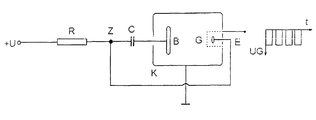
- this object is achieved by the modulator described in the patent claim, in that the switch known from the prior art is not provided as a technically independent unit, but rather is integrated into the implantation chamber in the form of an additional electrode which can be controlled via a shielding grid.
- the shielding grid which surrounds the electrode immersed in the plasma space, ensures, by applying controllable grid voltages, that the additional electrode is either insulated from the plasma or is in electrical contact with it. In the latter case, the discharge circuit of the capacitor is closed, analogously to the closed switch in the modulator described above.
- + U connects the positive pole of the high-voltage generator to the capacitor C via a resistor R, the second pole of which is connected to the processing table B within the implantation chamber K via a high-voltage bushing.
- the implantation chamber itself is at ground potential.
- the connection point Z lies between R and C, which in turn is connected to the additional electrode E within the implantation chamber K via a high-voltage bushing.
- This electrode is shielded from the plasma P by a grid G to which a negative control voltage UG can be applied.
- the electrode E and the grid G surrounding it are arranged at a sufficient distance from the material to be treated in the implantation chamber K and insulated from the latter.
- the second connection of the capacitor connected to the processing table is also kept at the potential of the implantation chamber K (ground potential) by the plasma, ie the capacitor is charged by the high voltage source as long as the electrode E is isolated from the plasma by means of a negative grid voltage UG.
- the electrical insulation of the electrode E from the plasma is achieved in the following way: Depending on the electron temperature and the mesh size of the shielding grid, the negative grid voltage of the shielding grid is determined in such a way that the thermal electrons of the plasma cannot pass through the shielding grid, which is why about ten - Up to a hundred times the value of the electron temperature is required.
- the processing table B and also the treatment material located thereon are at a negative potential with respect to the surrounding plasma, positively charged ions are accelerated from the plasma in the direction of the processing table B and implanted into the treatment material as a result of the speed obtained by the potential difference between the plasma and the processing table B.
- This also closes the discharge circuit of the capacitor C, since the positively charged ions reach the processing table and the material to be treated and the electrons to the electrode E are accelerated.
- the negative grid voltage UG to the shielding grid of the electrode E the electrode E is electrically isolated again from the plasma in the manner described above, whereby the discharge process of the capacitor is interrupted.
- the processing table is held at plasma potential again by the plasma.
- the implantation process is finished and the capacitor is recharged.
- the duration and the repetition rate of such an implantation cycle are variable.
- the discharge times of the capacitor C and thus the implantation times are usually a few ⁇ s to 100 ⁇ s, while the repetition rates are up to several kHz.
- the capacitance of the capacitor C is dimensioned such that only a partial discharge of the capacitor takes place during the discharge process. If only as many electrons are extracted from the plasma as ions are implanted during the discharge phase of the capacitor C, the charge carrier balance of the plasma is not disturbed. When the ions strike the material to be treated, however, secondary electrons are also triggered which, if no secondary electron suppression is provided, are accelerated away from the material to be treated towards the chamber wall due to the given potential difference.
- the charge carrier balance of the plasma also balances out here, however, since the plasma potential shifts towards positive values, as a result of which the current of the thermal electrons of the plasma to the chamber wall is correspondingly reduced. This compensation is also supported by the electrons released there when the secondary electrons strike the chamber wall.
- the size of the current generated by the accelerated ions and electrons depends on the plasma parameters and the potential difference between the processing table and the plasma. The current densities that usually occur are around 0.1 to 1 A / cm 2 and are highest at the beginning of the pulse. After several ⁇ s, the current density drops to a stationary value.
Landscapes
- Physics & Mathematics (AREA)
- Engineering & Computer Science (AREA)
- Plasma & Fusion (AREA)
- Chemical & Material Sciences (AREA)
- Analytical Chemistry (AREA)
- Physical Vapour Deposition (AREA)
- Drying Of Semiconductors (AREA)
- Crystals, And After-Treatments Of Crystals (AREA)
- Ceramic Products (AREA)
- Electron Sources, Ion Sources (AREA)
Claims (1)
- Modulateur pour la commande de l'implantation d'ions par immersion dans un plasma et pulsée à haute tension, dans lequel un plateau de traitement disposé à l'intérieur d'une chambre d'implantation est relié à une source de haute tension par un condensateur et par une résistance, caractérisé par le fait que le pôle du condensateur qui n'est pas dirigé vers le plateau de traitement est relié à une électrode supplémentaire disposée dans la chambre d'implantation et protégée contre le plasma par une grille, et que la grille pour sa part est reliée à un générateur de pulsations servant à la génération de pulsations de tension négative dans la plage de 1 à 2000 V.
Applications Claiming Priority (3)
| Application Number | Priority Date | Filing Date | Title |
|---|---|---|---|
| DE19702294A DE19702294A1 (de) | 1997-01-23 | 1997-01-23 | Modulator für die Plasmaimmersions-Ionenimplantation |
| DE19702294 | 1997-01-23 | ||
| PCT/DE1998/000144 WO1998033200A1 (fr) | 1997-01-23 | 1998-01-17 | Modulateur pour l'implantation d'ions par immersion dans un plasma |
Publications (2)
| Publication Number | Publication Date |
|---|---|
| EP0954875A1 EP0954875A1 (fr) | 1999-11-10 |
| EP0954875B1 true EP0954875B1 (fr) | 2003-01-02 |
Family
ID=7818138
Family Applications (1)
| Application Number | Title | Priority Date | Filing Date |
|---|---|---|---|
| EP98905260A Expired - Lifetime EP0954875B1 (fr) | 1997-01-23 | 1998-01-17 | Modulateur pour l'implantation d'ions par immersion dans un plasma |
Country Status (7)
| Country | Link |
|---|---|
| US (1) | US6205948B1 (fr) |
| EP (1) | EP0954875B1 (fr) |
| JP (1) | JP3506717B2 (fr) |
| AT (1) | ATE230519T1 (fr) |
| AU (1) | AU6089498A (fr) |
| DE (2) | DE19702294A1 (fr) |
| WO (1) | WO1998033200A1 (fr) |
Families Citing this family (4)
| Publication number | Priority date | Publication date | Assignee | Title |
|---|---|---|---|---|
| US6237527B1 (en) * | 1999-08-06 | 2001-05-29 | Axcelis Technologies, Inc. | System for improving energy purity and implant consistency, and for minimizing charge accumulation of an implanted substrate |
| US7838842B2 (en) * | 1999-12-13 | 2010-11-23 | Semequip, Inc. | Dual mode ion source for ion implantation |
| WO2005042064A1 (fr) * | 2003-10-31 | 2005-05-12 | Ventracor Limited | Pompe a sang amelioree comprenant des composants polymeres |
| US20050205211A1 (en) * | 2004-03-22 | 2005-09-22 | Vikram Singh | Plasma immersion ion implantion apparatus and method |
Family Cites Families (11)
| Publication number | Priority date | Publication date | Assignee | Title |
|---|---|---|---|---|
| US5212425A (en) * | 1990-10-10 | 1993-05-18 | Hughes Aircraft Company | Ion implantation and surface processing method and apparatus |
| WO1993018201A1 (fr) * | 1992-03-02 | 1993-09-16 | Varian Associates, Inc. | Procede d'implantation du plasma et equipement |
| US5330800A (en) * | 1992-11-04 | 1994-07-19 | Hughes Aircraft Company | High impedance plasma ion implantation method and apparatus |
| US5572038A (en) * | 1993-05-07 | 1996-11-05 | Varian Associates, Inc. | Charge monitor for high potential pulse current dose measurement apparatus and method |
| KR100302167B1 (ko) * | 1993-11-05 | 2001-11-22 | 히가시 데쓰로 | 플라즈마처리장치및플라즈마처리방법 |
| JP3060876B2 (ja) * | 1995-02-15 | 2000-07-10 | 日新電機株式会社 | 金属イオン注入装置 |
| DE19538903A1 (de) * | 1995-10-19 | 1997-04-24 | Rossendorf Forschzent | Verfahren zur Implantation von Ionen in leitende bzw. halbleitende Werkstücke mittels Plasmaimmersionsionenimplantation (P III) und Implantationskammer zur Durchführung des Verfahrens |
| US5911832A (en) * | 1996-10-10 | 1999-06-15 | Eaton Corporation | Plasma immersion implantation with pulsed anode |
| US5654043A (en) * | 1996-10-10 | 1997-08-05 | Eaton Corporation | Pulsed plate plasma implantation system and method |
| JP3301357B2 (ja) * | 1997-08-26 | 2002-07-15 | 株式会社村田製作所 | 平行平板型プラズマcvd装置 |
| US6050218A (en) * | 1998-09-28 | 2000-04-18 | Eaton Corporation | Dosimetry cup charge collection in plasma immersion ion implantation |
-
1997
- 1997-01-23 DE DE19702294A patent/DE19702294A1/de not_active Withdrawn
-
1998
- 1998-01-17 WO PCT/DE1998/000144 patent/WO1998033200A1/fr not_active Ceased
- 1998-01-17 US US09/242,546 patent/US6205948B1/en not_active Expired - Fee Related
- 1998-01-17 EP EP98905260A patent/EP0954875B1/fr not_active Expired - Lifetime
- 1998-01-17 DE DE59806816T patent/DE59806816D1/de not_active Expired - Fee Related
- 1998-01-17 JP JP53148398A patent/JP3506717B2/ja not_active Expired - Fee Related
- 1998-01-17 AU AU60894/98A patent/AU6089498A/en not_active Abandoned
- 1998-01-17 AT AT98905260T patent/ATE230519T1/de not_active IP Right Cessation
Also Published As
| Publication number | Publication date |
|---|---|
| JP3506717B2 (ja) | 2004-03-15 |
| EP0954875A1 (fr) | 1999-11-10 |
| US6205948B1 (en) | 2001-03-27 |
| DE59806816D1 (de) | 2003-02-06 |
| JP2001511293A (ja) | 2001-08-07 |
| AU6089498A (en) | 1998-08-18 |
| DE19702294A1 (de) | 1998-07-30 |
| WO1998033200A1 (fr) | 1998-07-30 |
| ATE230519T1 (de) | 2003-01-15 |
Similar Documents
| Publication | Publication Date | Title |
|---|---|---|
| EP0553410B1 (fr) | Dispositif pour le revêtement d'un substrat, en particulier avec des couches non-électroconductrices | |
| DE69123430T2 (de) | Verfahren und Gerät zur Ionenimplantierung und Oberflächenbehandlung | |
| DE19651811B4 (de) | Vorrichtung zum Belegen eines Substrats mit dünnen Schichten | |
| EP0534068B1 (fr) | Equipement utilisé dans la technique des plasmas et du traitement des surfaces | |
| EP0502242B1 (fr) | Dispositif pour pulverisation réactif | |
| DE1515294C3 (de) | Trioden-Anordnung zur Zerstäubung von Stoffen mittels einer elektrischen Niederspannungsentladung | |
| EP0339554A2 (fr) | Source de faisceau ionique à haute fréquence | |
| EP0529259A1 (fr) | Appareil pour le traitement de substrats | |
| DE882769C (de) | Verfahren und Einrichtung zur Trennung geladener Teilchen von verschiedenem e/m-Verhaeltnis | |
| EP1864313A2 (fr) | Generateur de plasma sous vide | |
| EP0275018A2 (fr) | Procédé et appareil pour le revêtement de pièces conductrices par une décharge à arc | |
| CH689767A5 (de) | Verfahren zur Werkstueckbehandlung in einer Vakuumatmosphaere und Vakuumbehandlungsanlage. | |
| DE3802852C2 (fr) | ||
| DE69112166T2 (de) | Plasmaquellenvorrichtung für Ionenimplantierung. | |
| DE4223505C1 (de) | Einrichtung zum aufbringen elektrisch schlecht leitender oder isolierender schichten durch reaktives magnetronsputtern | |
| EP0954875B1 (fr) | Modulateur pour l'implantation d'ions par immersion dans un plasma | |
| DE4239218C2 (de) | Anordnung zum Verhindern von Überschlägen in einem Plasma-Prozeßraum | |
| EP0277341B1 (fr) | Dispositif d'application d'un arc | |
| DE102009051056B4 (de) | Verfahren zum Wiederherstellen des Betriebszustandes der Entladung beim Magnetronsputtern und Schaltung zur Durchführung des Verfahrens | |
| AT523882B1 (de) | Verfahren und Vorrichtung zum Betreiben einer Flüssigmetall-Ionenquelle oder Flüssigmetall-Elektronenquelle sowie Flüssigmetall-Ionenquelle oder Flüssigmetall-Elektronenquelle | |
| EP0053107A1 (fr) | Procede de commande d'un canon electronique a haute stabilite pour le faconnage de materiaux. | |
| DE10240337B4 (de) | Vorrichtung und Verfahren zur Separation von Partikeln aus einem von einem Target zur Beschichtung eines Substrates erzeugten Plasma im Vakuum | |
| DE19538903A1 (de) | Verfahren zur Implantation von Ionen in leitende bzw. halbleitende Werkstücke mittels Plasmaimmersionsionenimplantation (P III) und Implantationskammer zur Durchführung des Verfahrens | |
| EP0317634A1 (fr) | Dispositif d'alimentation d'electrofiltres pour le nettoyage des gaz | |
| DE10303428A1 (de) | Verfahren und Einrichtung zur plasmaaktivierten Schichtabscheidung durch Kathodenzerstäubung nach dem Magnetron-Prinzip |
Legal Events
| Date | Code | Title | Description |
|---|---|---|---|
| PUAI | Public reference made under article 153(3) epc to a published international application that has entered the european phase |
Free format text: ORIGINAL CODE: 0009012 |
|
| 17P | Request for examination filed |
Effective date: 19990217 |
|
| AK | Designated contracting states |
Kind code of ref document: A1 Designated state(s): AT BE CH DE FI FR GB IT LI LU SE |
|
| GRAG | Despatch of communication of intention to grant |
Free format text: ORIGINAL CODE: EPIDOS AGRA |
|
| GRAG | Despatch of communication of intention to grant |
Free format text: ORIGINAL CODE: EPIDOS AGRA |
|
| GRAH | Despatch of communication of intention to grant a patent |
Free format text: ORIGINAL CODE: EPIDOS IGRA |
|
| 17Q | First examination report despatched |
Effective date: 20020207 |
|
| RAP1 | Party data changed (applicant data changed or rights of an application transferred) |
Owner name: FORSCHUNGSZENTRUM ROSSENDORF E.V. |
|
| GRAH | Despatch of communication of intention to grant a patent |
Free format text: ORIGINAL CODE: EPIDOS IGRA |
|
| GRAA | (expected) grant |
Free format text: ORIGINAL CODE: 0009210 |
|
| AK | Designated contracting states |
Kind code of ref document: B1 Designated state(s): AT BE CH DE FI FR GB IT LI LU SE |
|
| PG25 | Lapsed in a contracting state [announced via postgrant information from national office to epo] |
Ref country code: IT Free format text: LAPSE BECAUSE OF FAILURE TO SUBMIT A TRANSLATION OF THE DESCRIPTION OR TO PAY THE FEE WITHIN THE PRESCRIBED TIME-LIMIT;WARNING: LAPSES OF ITALIAN PATENTS WITH EFFECTIVE DATE BEFORE 2007 MAY HAVE OCCURRED AT ANY TIME BEFORE 2007. THE CORRECT EFFECTIVE DATE MAY BE DIFFERENT FROM THE ONE RECORDED. Effective date: 20030102 Ref country code: FI Free format text: LAPSE BECAUSE OF FAILURE TO SUBMIT A TRANSLATION OF THE DESCRIPTION OR TO PAY THE FEE WITHIN THE PRESCRIBED TIME-LIMIT Effective date: 20030102 |
|
| REF | Corresponds to: |
Ref document number: 230519 Country of ref document: AT Date of ref document: 20030115 Kind code of ref document: T |
|
| REG | Reference to a national code |
Ref country code: GB Ref legal event code: FG4D Free format text: 20030102:NOT ENGLISH |
|
| REG | Reference to a national code |
Ref country code: CH Ref legal event code: EP |
|
| PG25 | Lapsed in a contracting state [announced via postgrant information from national office to epo] |
Ref country code: LU Free format text: LAPSE BECAUSE OF NON-PAYMENT OF DUE FEES Effective date: 20030117 Ref country code: AT Free format text: LAPSE BECAUSE OF NON-PAYMENT OF DUE FEES Effective date: 20030117 |
|
| PG25 | Lapsed in a contracting state [announced via postgrant information from national office to epo] |
Ref country code: LI Free format text: LAPSE BECAUSE OF NON-PAYMENT OF DUE FEES Effective date: 20030131 Ref country code: CH Free format text: LAPSE BECAUSE OF NON-PAYMENT OF DUE FEES Effective date: 20030131 |
|
| REF | Corresponds to: |
Ref document number: 59806816 Country of ref document: DE Date of ref document: 20030206 Kind code of ref document: P |
|
| PG25 | Lapsed in a contracting state [announced via postgrant information from national office to epo] |
Ref country code: SE Free format text: LAPSE BECAUSE OF FAILURE TO SUBMIT A TRANSLATION OF THE DESCRIPTION OR TO PAY THE FEE WITHIN THE PRESCRIBED TIME-LIMIT Effective date: 20030402 |
|
| GBT | Gb: translation of ep patent filed (gb section 77(6)(a)/1977) |
Effective date: 20030508 |
|
| ET | Fr: translation filed | ||
| REG | Reference to a national code |
Ref country code: CH Ref legal event code: PL |
|
| PLBE | No opposition filed within time limit |
Free format text: ORIGINAL CODE: 0009261 |
|
| STAA | Information on the status of an ep patent application or granted ep patent |
Free format text: STATUS: NO OPPOSITION FILED WITHIN TIME LIMIT |
|
| 26N | No opposition filed |
Effective date: 20031003 |
|
| PGFP | Annual fee paid to national office [announced via postgrant information from national office to epo] |
Ref country code: BE Payment date: 20041022 Year of fee payment: 8 |
|
| PGFP | Annual fee paid to national office [announced via postgrant information from national office to epo] |
Ref country code: FR Payment date: 20041230 Year of fee payment: 8 |
|
| PGFP | Annual fee paid to national office [announced via postgrant information from national office to epo] |
Ref country code: GB Payment date: 20050112 Year of fee payment: 8 |
|
| PGFP | Annual fee paid to national office [announced via postgrant information from national office to epo] |
Ref country code: DE Payment date: 20050217 Year of fee payment: 8 |
|
| PG25 | Lapsed in a contracting state [announced via postgrant information from national office to epo] |
Ref country code: GB Free format text: LAPSE BECAUSE OF NON-PAYMENT OF DUE FEES Effective date: 20060117 |
|
| PG25 | Lapsed in a contracting state [announced via postgrant information from national office to epo] |
Ref country code: FR Free format text: LAPSE BECAUSE OF NON-PAYMENT OF DUE FEES Effective date: 20060131 Ref country code: BE Free format text: LAPSE BECAUSE OF NON-PAYMENT OF DUE FEES Effective date: 20060131 |
|
| PG25 | Lapsed in a contracting state [announced via postgrant information from national office to epo] |
Ref country code: DE Free format text: LAPSE BECAUSE OF NON-PAYMENT OF DUE FEES Effective date: 20060801 |
|
| GBPC | Gb: european patent ceased through non-payment of renewal fee |
Effective date: 20060117 |
|
| REG | Reference to a national code |
Ref country code: FR Ref legal event code: ST Effective date: 20060929 |
|
| BERE | Be: lapsed |
Owner name: FORSCHUNGSZENTRUM *ROSSENDORF E.V. Effective date: 20060131 |