EP0955558A2 - Optischer Reflektor für multiple Wellenlängen - Google Patents
Optischer Reflektor für multiple Wellenlängen Download PDFInfo
- Publication number
- EP0955558A2 EP0955558A2 EP99303555A EP99303555A EP0955558A2 EP 0955558 A2 EP0955558 A2 EP 0955558A2 EP 99303555 A EP99303555 A EP 99303555A EP 99303555 A EP99303555 A EP 99303555A EP 0955558 A2 EP0955558 A2 EP 0955558A2
- Authority
- EP
- European Patent Office
- Prior art keywords
- grating
- gratings
- reflector
- wavelength
- phase
- Prior art date
- Legal status (The legal status is an assumption and is not a legal conclusion. Google has not performed a legal analysis and makes no representation as to the accuracy of the status listed.)
- Granted
Links
Images


Classifications
-
- G—PHYSICS
- G02—OPTICS
- G02B—OPTICAL ELEMENTS, SYSTEMS OR APPARATUS
- G02B6/00—Light guides; Structural details of arrangements comprising light guides and other optical elements, e.g. couplings
- G02B6/10—Light guides; Structural details of arrangements comprising light guides and other optical elements, e.g. couplings of the optical waveguide type
- G02B6/12—Light guides; Structural details of arrangements comprising light guides and other optical elements, e.g. couplings of the optical waveguide type of the integrated circuit kind
- G02B6/122—Basic optical elements, e.g. light-guiding paths
-
- H—ELECTRICITY
- H01—ELECTRIC ELEMENTS
- H01S—DEVICES USING THE PROCESS OF LIGHT AMPLIFICATION BY STIMULATED EMISSION OF RADIATION [LASER] TO AMPLIFY OR GENERATE LIGHT; DEVICES USING STIMULATED EMISSION OF ELECTROMAGNETIC RADIATION IN WAVE RANGES OTHER THAN OPTICAL
- H01S5/00—Semiconductor lasers
- H01S5/10—Construction or shape of the optical resonator, e.g. extended or external cavity, coupled cavities, bent-guide, varying width, thickness or composition of the active region
- H01S5/12—Construction or shape of the optical resonator, e.g. extended or external cavity, coupled cavities, bent-guide, varying width, thickness or composition of the active region the resonator having a periodic structure, e.g. in distributed feedback [DFB] lasers
-
- G—PHYSICS
- G02—OPTICS
- G02B—OPTICAL ELEMENTS, SYSTEMS OR APPARATUS
- G02B6/00—Light guides; Structural details of arrangements comprising light guides and other optical elements, e.g. couplings
- G02B6/10—Light guides; Structural details of arrangements comprising light guides and other optical elements, e.g. couplings of the optical waveguide type
- G02B6/12—Light guides; Structural details of arrangements comprising light guides and other optical elements, e.g. couplings of the optical waveguide type of the integrated circuit kind
- G02B2006/12083—Constructional arrangements
- G02B2006/12104—Mirror; Reflectors or the like
-
- G—PHYSICS
- G02—OPTICS
- G02B—OPTICAL ELEMENTS, SYSTEMS OR APPARATUS
- G02B6/00—Light guides; Structural details of arrangements comprising light guides and other optical elements, e.g. couplings
- G02B6/10—Light guides; Structural details of arrangements comprising light guides and other optical elements, e.g. couplings of the optical waveguide type
- G02B6/12—Light guides; Structural details of arrangements comprising light guides and other optical elements, e.g. couplings of the optical waveguide type of the integrated circuit kind
- G02B2006/12083—Constructional arrangements
- G02B2006/12107—Grating
-
- G—PHYSICS
- G02—OPTICS
- G02B—OPTICAL ELEMENTS, SYSTEMS OR APPARATUS
- G02B6/00—Light guides; Structural details of arrangements comprising light guides and other optical elements, e.g. couplings
- G02B6/02—Optical fibres with cladding with or without a coating
- G02B6/02057—Optical fibres with cladding with or without a coating comprising gratings
- G02B6/02076—Refractive index modulation gratings, e.g. Bragg gratings
- G02B6/0208—Refractive index modulation gratings, e.g. Bragg gratings characterised by their structure, wavelength response
- G02B6/02085—Refractive index modulation gratings, e.g. Bragg gratings characterised by their structure, wavelength response characterised by the grating profile, e.g. chirped, apodised, tilted, helical
-
- H—ELECTRICITY
- H01—ELECTRIC ELEMENTS
- H01S—DEVICES USING THE PROCESS OF LIGHT AMPLIFICATION BY STIMULATED EMISSION OF RADIATION [LASER] TO AMPLIFY OR GENERATE LIGHT; DEVICES USING STIMULATED EMISSION OF ELECTROMAGNETIC RADIATION IN WAVE RANGES OTHER THAN OPTICAL
- H01S5/00—Semiconductor lasers
- H01S5/10—Construction or shape of the optical resonator, e.g. extended or external cavity, coupled cavities, bent-guide, varying width, thickness or composition of the active region
- H01S5/12—Construction or shape of the optical resonator, e.g. extended or external cavity, coupled cavities, bent-guide, varying width, thickness or composition of the active region the resonator having a periodic structure, e.g. in distributed feedback [DFB] lasers
- H01S5/1206—Construction or shape of the optical resonator, e.g. extended or external cavity, coupled cavities, bent-guide, varying width, thickness or composition of the active region the resonator having a periodic structure, e.g. in distributed feedback [DFB] lasers having a non constant or multiplicity of periods
- H01S5/1209—Sampled grating
-
- H—ELECTRICITY
- H01—ELECTRIC ELEMENTS
- H01S—DEVICES USING THE PROCESS OF LIGHT AMPLIFICATION BY STIMULATED EMISSION OF RADIATION [LASER] TO AMPLIFY OR GENERATE LIGHT; DEVICES USING STIMULATED EMISSION OF ELECTROMAGNETIC RADIATION IN WAVE RANGES OTHER THAN OPTICAL
- H01S5/00—Semiconductor lasers
- H01S5/10—Construction or shape of the optical resonator, e.g. extended or external cavity, coupled cavities, bent-guide, varying width, thickness or composition of the active region
- H01S5/12—Construction or shape of the optical resonator, e.g. extended or external cavity, coupled cavities, bent-guide, varying width, thickness or composition of the active region the resonator having a periodic structure, e.g. in distributed feedback [DFB] lasers
- H01S5/124—Construction or shape of the optical resonator, e.g. extended or external cavity, coupled cavities, bent-guide, varying width, thickness or composition of the active region the resonator having a periodic structure, e.g. in distributed feedback [DFB] lasers incorporating phase shifts
- H01S5/1246—Construction or shape of the optical resonator, e.g. extended or external cavity, coupled cavities, bent-guide, varying width, thickness or composition of the active region the resonator having a periodic structure, e.g. in distributed feedback [DFB] lasers incorporating phase shifts plurality of phase shifts
Definitions
- This invention relates to a multi-wavelength optical reflector which includes a diffraction grating structure and a method of making such a reflector. More especially, although not exclusively, the invention relates to an optical reflector suitable for use with, or as part of, a wavelength division multiplexed (WDM) optical communications system.
- WDM wavelength division multiplexed
- Narrowband optical reflectors/filters are important for a number of applications in optical telecommunications and signal processing including multiple channel optical telecommunications networks using wavelength division multiplexing (WDM).
- WDM wavelength division multiplexing
- Such networks can provide advanced features, such as wavelength routing, wavelength switching and wavelength conversion, adding and dropping of channels and wavelength manipulation in much the same way as time slot manipulation in time division multiplexed systems.
- WDM is rapidly emerging as a key technology for optical networking but implementing it requires the development and optimisation of many of the optical devices required within such systems.
- tuneable optical sources are required which can provide the many different wavelengths required for the many different channels.
- filters such as comb filters and passband filters are required to exclude spurious signals and wavelength monitoring is required to avoid straying off channel and contaminating the network.
- Such networks must include optical amplifiers, such as the erbium doped fibre amplifier, which currently limits the overall bandwidth to approximately 35nm. As a consequence much work is tending to concentrate on developing optical components which operate within the erbium bandwidth window.
- a laser suitable for an optical telecommunications network is a Distributed Feedback (DFB) laser diode.
- DFB Distributed Feedback
- the grating can be formed as a corrugation which acts as a periodically varying optical waveguide boundary and allows coupling between the forward and backward propagating waves.
- a DFB laser diode incorporating such a grating structure operates in a first-order spatial harmonic mode whether directly in the first-order or indirectly at the first-order spatial harmonic component of a multiple order grating.
- DFB lasers it is common for DFB lasers to include end reflectors, such that the longitudinal mode spectrum is asymmetrically distributed about the Bragg wavelength. This type of DFB laser has one dominant mode and therefore has a stable output at a given wavelength.
- US 4 896 325 proposes a wavelength tuneable laser having sampled gratings at the front and rear of its gain region.
- the gratings produce slightly different reflection combs which provide feedback into the device.
- the gratings can be current tuned in wavelength with respect to each other. Coincidence of a maximum from each of the front and rear gratings is referred to as supermode.
- To switch the device between supermodes requires a small electrical current into one of the gratings to cause a different pair of maxima to coincide in the manner of a vernier.
- the diffraction gratings should ideally have a flat reflection spectrum, that is it should comprise a plurality of reflection maxima of equal intensity.
- the reflection spectra of the known sampled grating structures have a Gaussian type envelope which limits the total optical bandwidth over which the laser can reliably operate as a single mode device.
- the output power of the laser as a function of wavelength is not uniform. A need exists therefore for a grating structure having an improved reflection spectrum.
- US 5325392 discloses a distributed reflector structure which comprises a diffraction grating having a repeating unit of constant length which defines a modulation period and at least one of a number of parameters that determines an optical reflectivity of the grating and varies in dependence on its position in each of the repeating units.
- the parameter comprises changing (shortening or lengthening) the pitch of the grating within a single grating period at the selected positions in a repeating unit. These changes in pitch are equivalent to a progressive change in the phase and the resulting structure is thus a chirped grating structure. Since the device requires a number of gradual and progressive changes in pitch, the only techniques available to make the device are electron beam techniques which are expensive and do not lend themselves to large scale production.
- the present invention has arisen in an endeavour to provide a multi-wavelength comb reflector filter for use in a WDM system which in part at least overcomes the limitations of the known reflectors.
- a multi-wavelength optical reflector comprises: a diffraction grating structure comprising a plurality of repeat grating units in which each grating unit comprises a series of adjacent diffraction gratings having the same pitch, characterised in that grating units and adjacent gratings within a grating unit are separated by a phase change of substantially pi ( ⁇ ) radians and wherein at least two of the gratings within a grating unit have different lengths, the lengths being selected so as to provide a predetermined reflection spectrum. Since the phase changes within a grating unit are substantially pi radians this enables the device to be readily manufactured using holographic and photolithographic techniques.
- a predetermined reflection spectrum is one in which the reflectivity of individual reflection maxima are chosen to provide an optimum response from the device for its particular application.
- a predetermined reflection spectrum has a number of individual reflection maxima which have substantially equal reflectivities.
- adjacent grating units and/or adjacent gratings within a grating unit are substantially contiguous.
- small gaps between adjacent grating units and/or adjacent gratings may be present when using phase mask holographic techniques to define the phase shifts, such gaps are not found to affect the reflection spectrum appreciably.
- the lengths of the gratings are selected by superposing a plurality of periodic variations having different periods to form a periodic waveform having a multi-lobed envelope and the relative lengths of the gratings are selected to correspond with the relative lengths at which the envelope tends to zero.
- phase shifts are preferably imparted to individuals of the plurality of periodic variations.
- pairs of the phase shifts are imparted to individuals of the plurality of variations, the pairs of phase shifts having equal magnitude but opposite sign.
- a grating structure constructed having grating lengths selected in this manner is found to have a more uniform reflection spectrum.
- the periodic variations are not all in phase at any point along the length over which they are superposed. It will be appreciated that the described selection method can alternatively be used to determined an initial position for the phase shifts and the phase shifts optimised using an iterative process to obtain the desired reflection spectrum.
- the reflector comprises a waveguide device though it can alternatively be fabricated as a transmission grating or could for example be incorporated as part of a Fabry Perót cavity.
- the reflector of the present invention can be incorporated into a filter or a laser or can be incorporated as part of a wavelength division multiplexer or demultiplexer.
- a method of making a multi-wavelength optical reflector as described above characterised in that a single exposure step is required to produce a pattern from which the diffraction grating structure can be obtained.
- a single exposure step is required to produce a pattern from which the diffraction grating structure can be obtained.
- the reflector comprises a substrate 12 of Indium Phosphide (InP); an optical guiding layer 14 of Indium Gallium Arsenide Phosphide (InGaAsP) and an upper layer 16 of Indium Phosphide. Since the substrate 12 and upper layer 16 are of a lower refractive index (3.17) to that of the optical layer 14 (3.23) this ensures that light is confined to the guiding layer 14.
- InP Indium Phosphide
- InGaAsP Indium Gallium Arsenide Phosphide
- a grating structure 18 is formed in the outermost surface of the upper layer 16, that is the surface distal from the junction between the layers 14 and 16 by for example dry etching using a photoresist grating as a mask.
- a grating structure in close proximity to a waveguide will cause distributed reflections of light propagating through the optical layer 14 such that light is reflected at set wavelengths in dependence upon the grating structure 18.
- the grating structure 18 of the present invention comprises a number of repeat units 20 each of which comprises three Bragg gratings of identical constant pitch which are of different lengths 22, 24, 26 respectively.
- Adjacent repeat units 20 and adjacent gratings within a unit 20 are defined by phase shifts of ⁇ radians (that is 180 degrees) in the periodic amplitude variation of the grating structure 18. These phase shifts are denoted by the boundaries 28 in Figure 1.
- the lengths of the gratings 22, 24, 26 are 0.58, 0.20 and 0.22 respectively. It will be appreciated that in the context of the present invention the lengths are different in a direction of propagation of light through the optical layer 14. For clarity, in the schematic representation of Figure 1, only two repeat units 20 are illustrated though in practice typically five or more repeat units 20 are present.
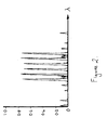
- the reflection spectrum that is a plot of normalised reflectivity versus wavelength of light guided by the waveguide, for the reflector 10 is shown in Figure 2. It should be noted that the reflection spectrum comprises six reflection maxima, which are narrow and high and are all of substantially the same reflectivity.
- the width and height of the reflection maxima are determined by the number of repeat units within the grating structure. The more repeat units there are, the narrower and higher are the reflection maxima, that is the extinction ratios and spectral noise are better.
- the relative heights of the maxima that is how flat the reflection spectrum is, are determined by the lengths of the gratings 22, 24, 26 within a repeat unit 20.
- the grating structure 18 is configured to provide adequate side-mode suppression of minor peaks by appropriate selection of the length of the gratings 22, 24, 26.
- the number of gratings within a repeat unit depends on the number of reflection maxima required in the desired reflection spectrum. For example for the specific example described the six reflection maxima are provided by the three gratings in each repeat unit.
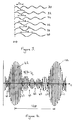
- the lengths of the gratings (more precisely, the position of the phase shifts) within a repeat unit can be selected to produce a predetermined response it is instructive to consider the grating structure 18 as being analagous to the superposition of a number of periodic variations in magnitude, for example periodic variations in intensity.
- FIG 3 there are shown six periodic variations 30, 32, 34, 36, 38, and 40 having respective different periods of ⁇ 1 , ⁇ 2 , ⁇ 3 , ⁇ 4 , ⁇ 5 and ⁇ 6 and corresponding frequencies F 1 , F 2 , F 3 , F 4 , F 5 and F 6 respectively.
- This waveform consists of a relatively rapidly varying underlying waveform 42 of spatial frequency F 0 (where which is magnitude modulated by a relatively slowly varying envelope 44 having a super period 1/ ⁇ F.
- the envelope 44 is periodic and has a number of maxima separated by crossover points 45 at which the envelope 44 tends to zero.
- the envelope 44 can be applied in the making of a grating structure in the form of a plurality of adjacent gratings of identical constant pitch 1/F 0 which are separated by phase shifts of ⁇ radians. The positions of the phase shifts are selected to correspond with the positions of the crossover points 45 and the super period 1/ ⁇ F corresponds with the length of the repeat units 20.
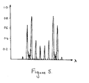
- the envelope waveform 44 is written into a medium as a constant amplitude square wave grating of constant pitch 1/F 0 with phase changes of ⁇ radians located at the crossover points 45 a multi-wavelength grating is formed whose reflection spectrum is shown in Figure 5. It should be noted that there is considerable variation in the reflectivity values of the reflection maxima as compared to the spectrum of Figure 2.
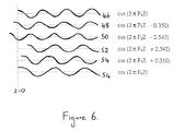
- the other periodic variations have applied to them equal and opposite phase shifts.
- This is represented graphically in Figure 6 for six periodic variations 46, 48, 50, 52, 54 and 56 of differing respective periods ⁇ 1 to ⁇ 6 and frequencies F 1 to F 6 .
- phase shifted intensity variations are superposed they produce the multi-wavelength waveform depicted in Figure 7 which, in common with that of Figure 3, consists of a rapidly varying waveform which is modulated by a slowly varying envelope 58.
- envelope waveform 58 is shown in Figure 7. It is to be noted that the phase of the rapidly varying waveform changes by ⁇ radians at the crossover points 60 where the envelope waveform tends to zero. It should further be noted that there is no phase change at maxima and minima points 62.
- the tuneable laser comprises within an optical layer 14 a laser cavity 64 which is defined by an active region 66 and two multi-wavelength diffraction gratings 68 and 70 located at a respective end of the active region 66.
- the multi-wavelength diffraction gratings 68, 70 are configured such that the reflection maxima in each grating have different spacings so that only one of the reflection maxima of each multi-wavelength diffraction grating 68, 70 can be in correspondence, and thus provide a low loss window, at any one time.
- the multi-wavelength diffraction gratings 68, 70 act as a vernier.
- a vernier circuit is provided which applies an electrical tuning current to the multi-wavelength diffraction gratings 68, 70 to shift the reflection maxima with respect to one another. In this way the laser can be tuned to emit light at a desired wavelength.
- a quartz phase plate 72 is made using a well known photo-lithographic technique to define the phase steps in the grating structures 68, 70.
- Figure 9 shows only the first region 74 of the phase plate 72 for producing the grating 68 and how it is derived from the envelope of Figure 7.
- the phase plate has a stepped structure in which the steps are located at positions which correspond with the crossover points 60 of the envelope 58.
- the phase plate 72 also includes a second stepped region 76 for defining the second grating 70.
- the phase plate 72 is then used in a two-beam holographic exposure process to record the two multi-wavelength gratings 68 and 70 in the upper layer 16.
- the stepped regions 74, 76 of the phase plate 72 are separated by a mask region 78.
- the stepped region 74, 76 and mask region 78 represent a first exposure unit 80 for a first beam of light 82.
- Adjacent to the first exposure unit 80 the phase plate 72 is provided with a second exposure unit 84 for a second beam of light 86.
- the second exposure unit 84 comprises two windows 88 which are separated by a further mask region 90.
- the exposure units 80 and 84 are illuminated by respective UV coherent light beams 82 and 86, each having a wavelength of 351.1 nm, angularly separated by an angle ⁇ .
- the light beams 82 and 86 have regions of common incidence 92 and 94 on a photoresist layer 96 which is provided on the surface of the upper layer 16.
- the mask regions 78 and 90 serve so as to mask the active region 66 from the light beams 82 and 86. However, the photoresist is exposed on either side of the active region 66.
- the envelope waveform that is the series of ⁇ phase shifts, is written into the photoresist layer 96 as a result relative phase differences between the beams 82 and 86 which are introduced by the stepped region 74, 76.
- the underlying grating structure is generated by interference of the two light beams 82 and 86.
- the pitch or period of the underlying grating structure depends on the angle ⁇ between the beams 82, 86.
- a desired pitch may be readily obtained simply by altering ⁇ . As an example for a required operation at 1.55 ⁇ m ⁇ is equal to 94°3'.
- the photoresist layer 96 is developed and the upper layer 16 is then etched. As a result, multi-wavelength diffraction gratings are etched as physical surface relief diffraction gratings into the surface of the upper layer 16.
- the envelope 58 of Figure 7 has an intensity characteristic which, in the fabrication process discussed above, is difficult to provide as a corresponding intensity characteristic in the etched grating.
- the photoresist has a binary nature; that is, it resists when not exposed and does not resist when exposed. Therefore it is difficult to provide variation in the etch rate of the photoresist and thus variation in etch depth of the physical grating.
- the grating is an approximation of the envelope waveform rather than a perfect replica.
- multi-wavelength gratings according to the invention are generated theoretically with approximately located phase shifts.
- the locations of the phase shifts are then optimised by modelling to correct for any degradation introduced by not including the intensity information.
- the grating is only an approximation the resulting reflection spectrum is not degraded appreciably.
- the function I(z) (Eq. 4) represents an intensity pattern of optical exposure in a photoresist. Exposure is a highly non-linear process and has a threshold intensity I th . When the optical intensity exceeds I th the photoresist is developed to a depth d from its surface and can readily be etched to this depth. If I(z) is less than I th there is insufficient development to enable the surface photoresist to be etched away.
- the method of the invention thus provides a way of making a grating in a one-step process having a single exposure.
- the upper layer 16 would comprise a quaternary layer of InGaAsP into which the surface relief grating is formed and which is then buried by overgrowing with a layer of InP.
- the method of the present invention is particularly convenient for forming a grating structure having a series of phase shifts of pi radians, other fabrication methods can be used such as for example directly writing the grating structure using electron beam lithography.
Landscapes
- Physics & Mathematics (AREA)
- General Physics & Mathematics (AREA)
- Optics & Photonics (AREA)
- Engineering & Computer Science (AREA)
- Microelectronics & Electronic Packaging (AREA)
- Condensed Matter Physics & Semiconductors (AREA)
- Electromagnetism (AREA)
- Optical Integrated Circuits (AREA)
Applications Claiming Priority (2)
| Application Number | Priority Date | Filing Date | Title |
|---|---|---|---|
| GB9809583 | 1998-05-06 | ||
| GBGB9809583.9A GB9809583D0 (en) | 1998-05-06 | 1998-05-06 | Optical devices |
Publications (3)
| Publication Number | Publication Date |
|---|---|
| EP0955558A2 true EP0955558A2 (de) | 1999-11-10 |
| EP0955558A3 EP0955558A3 (de) | 2001-02-28 |
| EP0955558B1 EP0955558B1 (de) | 2012-10-31 |
Family
ID=10831483
Family Applications (1)
| Application Number | Title | Priority Date | Filing Date |
|---|---|---|---|
| EP99303555A Expired - Lifetime EP0955558B1 (de) | 1998-05-06 | 1999-05-06 | Optischer Reflektor für multiple Wellenlängen |
Country Status (3)
| Country | Link |
|---|---|
| US (1) | US6345135B1 (de) |
| EP (1) | EP0955558B1 (de) |
| GB (2) | GB9809583D0 (de) |
Cited By (8)
| Publication number | Priority date | Publication date | Assignee | Title |
|---|---|---|---|---|
| GB2379084A (en) * | 2001-08-24 | 2003-02-26 | Marconi Caswell Ltd | Surface emitting laser |
| GB2381123A (en) * | 2001-10-17 | 2003-04-23 | Marconi Caswell Ltd | Tuneable laser |
| FR2848679A1 (fr) * | 2002-12-16 | 2004-06-18 | Teem Photonics | Composant de filtrage en optique integree comprenant une gaine optique ainsi que son procede de realisation |
| US7149384B2 (en) | 2001-03-16 | 2006-12-12 | Redfern Optical Components Pty Ltd. | Grating design |
| GB2430760A (en) * | 2005-09-29 | 2007-04-04 | Bookham Technology Plc | Chirped Bragg grating structure |
| WO2007036750A1 (en) * | 2005-09-29 | 2007-04-05 | Bookham Technology Plc | Bragg grating reflection strength control |
| AU2002242460B2 (en) * | 2001-03-16 | 2007-07-12 | Tyco Electronics Pty Ltd | Grating design |
| CN104094486A (zh) * | 2011-11-09 | 2014-10-08 | 康宁股份有限公司 | 具有对称非周期移动的光栅相位的dbr激光二极管 |
Families Citing this family (30)
| Publication number | Priority date | Publication date | Assignee | Title |
|---|---|---|---|---|
| GB9809583D0 (en) * | 1998-05-06 | 1998-07-01 | Marconi Gec Ltd | Optical devices |
| US6909734B2 (en) | 1999-09-02 | 2005-06-21 | Agility Communications, Inc. | High-power, manufacturable sampled grating distributed Bragg reflector lasers |
| US6690693B1 (en) | 2000-05-04 | 2004-02-10 | Agility Communications, Inc. | Power and wavelength control of sampled grating distributed Bragg reflector lasers |
| US6937638B2 (en) * | 2000-06-09 | 2005-08-30 | Agility Communications, Inc. | Manufacturable sampled grating mirrors |
| US6788719B2 (en) | 2000-05-04 | 2004-09-07 | Agility Communications, Inc. | Open loop control of SGDBR lasers |
| US6590924B2 (en) * | 2000-05-04 | 2003-07-08 | Agility Communications, Inc. | Mirror and cavity designs for sampled grating distributed bragg reflector lasers |
| WO2002093701A1 (en) * | 2001-05-15 | 2002-11-21 | Agility Communications, Inc. | Controller calibration for small form factor sampled grating distributed bragg reflector laser |
| US7061943B2 (en) * | 2000-06-29 | 2006-06-13 | Agility Communications, Inc. | Controller calibration for small form factor sampled grating distributed Bragg reflector laser |
| JP2002090556A (ja) * | 2000-09-20 | 2002-03-27 | Sumitomo Electric Ind Ltd | 光導波路型回折格子素子、光導波路型回折格子素子製造方法、合分波モジュールおよび光伝送システム |
| AUPR335901A0 (en) * | 2001-02-26 | 2001-03-22 | Redfern Optical Components Pty Ltd | Multi channel grating design |
| US6954476B2 (en) * | 2001-05-15 | 2005-10-11 | Agility Communications, Inc. | Sampled grating distributed Bragg reflector laser controller |
| AUPS113102A0 (en) * | 2002-03-15 | 2002-04-18 | Redfern Optical Components Pty Ltd | Improved multi channel grating design |
| AU2003281701B2 (en) * | 2002-07-30 | 2009-05-21 | Tyco Electronics Pty Ltd | Improved multi-channel grating design technique |
| AU2002950462A0 (en) * | 2002-07-30 | 2002-09-12 | Redfern Optical Components Pty Ltd | Improved multi-channel grating design technique |
| JP2004219655A (ja) * | 2003-01-14 | 2004-08-05 | Sumitomo Electric Ind Ltd | 光導波路型回折格子素子製造方法および装置 |
| EP2021847A4 (de) * | 2006-04-24 | 2012-10-31 | Redfern Optical Components Pty Ltd | Verfahren zum entwurf optimierter mehrkanaliger gitterstrukturen |
| WO2008035321A2 (en) * | 2006-09-20 | 2008-03-27 | The Provost, Fellows And Scholars Of The College Of The Holy And Undivided Trinity Of Queen Elizabeth Near Dublin | Multisection ld having a ridge with voids for longitudinal mode control |
| GB2448162A (en) | 2007-04-03 | 2008-10-08 | Bookham Technology Plc | Tunable semiconductor laser |
| FR2915812B1 (fr) * | 2007-05-04 | 2009-06-12 | Saint Gobain | Ensemble de sous-reseaux diffusant la lumiere |
| GB2493988B (en) | 2011-08-26 | 2016-01-13 | Oclaro Technology Ltd | Monolithically integrated tunable semiconductor laser |
| US9209601B2 (en) | 2011-08-26 | 2015-12-08 | Oclaro Technology Ltd | Monolithically integrated tunable semiconductor laser |
| GB2507527A (en) | 2012-11-01 | 2014-05-07 | Oclaro Technology Ltd | Semiconductor DBR laser |
| WO2016144831A1 (en) | 2015-03-06 | 2016-09-15 | Apple Inc. | Independent control of emission wavelength and output power of a semiconductor laser |
| CN107624206B (zh) * | 2015-04-30 | 2022-05-27 | 苹果公司 | 包括集成调谐元件的游标效应dbr激光器 |
| CN113725725B (zh) | 2017-09-28 | 2025-05-02 | 苹果公司 | 使用量子阱混合技术的激光架构 |
| US11552454B1 (en) | 2017-09-28 | 2023-01-10 | Apple Inc. | Integrated laser source |
| US11171464B1 (en) | 2018-12-14 | 2021-11-09 | Apple Inc. | Laser integration techniques |
| US10855372B1 (en) * | 2019-10-16 | 2020-12-01 | Honeywell International Inc. | Systems and methods for reduction of optical signal line width |
| US12204155B2 (en) | 2021-09-24 | 2025-01-21 | Apple Inc. | Chip-to-chip optical coupling for photonic integrated circuits |
| US12426139B1 (en) | 2022-06-27 | 2025-09-23 | Apple Inc. | Feedback control of a diode element |
Family Cites Families (13)
| Publication number | Priority date | Publication date | Assignee | Title |
|---|---|---|---|---|
| US4622114A (en) * | 1984-12-20 | 1986-11-11 | At&T Bell Laboratories | Process of producing devices with photoelectrochemically produced gratings |
| US4896325A (en) | 1988-08-23 | 1990-01-23 | The Regents Of The University Of California | Multi-section tunable laser with differing multi-element mirrors |
| FR2677499A1 (fr) * | 1991-06-07 | 1992-12-11 | Alsthom Cge Alcatel | Laser semiconducteur monomodal a retroaction distribuee et son procede de fabrication. |
| US5325392A (en) | 1992-03-06 | 1994-06-28 | Nippon Telegraph And Telephone Corporation | Distributed reflector and wavelength-tunable semiconductor laser |
| US5400422A (en) | 1993-01-21 | 1995-03-21 | The United States Of America As Represented By The Secretary Of The Navy | Technique to prepare high-reflectance optical fiber bragg gratings with single exposure in-line or fiber draw tower |
| JP3086767B2 (ja) * | 1993-05-31 | 2000-09-11 | 株式会社東芝 | レ−ザ素子 |
| FR2728975A1 (fr) | 1994-12-28 | 1996-07-05 | Alcatel Submarcom | Filtre pour lumiere guidee et liaison optique incluant ce filtre |
| US5699378A (en) * | 1995-10-06 | 1997-12-16 | British Telecommunications Public Limited Company | Optical comb filters used with waveguide, laser and manufacturing method of same |
| US5668900A (en) * | 1995-11-01 | 1997-09-16 | Northern Telecom Limited | Taper shapes for sidelobe suppression and bandwidth minimization in distributed feedback optical reflection filters |
| US5715271A (en) * | 1996-08-01 | 1998-02-03 | Northern Telecom Limited | Polarization independent grating resonator filter |
| FR2752950B1 (fr) * | 1996-09-02 | 1998-10-09 | Alsthom Cge Alcatel | Filtre passe-bande inscrit dans un guide d'onde optique |
| KR100289042B1 (ko) * | 1997-12-23 | 2001-05-02 | 이계철 | 쌍격자구조를갖는수직결합형파장가변광필터 |
| GB9809583D0 (en) * | 1998-05-06 | 1998-07-01 | Marconi Gec Ltd | Optical devices |
-
1998
- 1998-05-06 GB GBGB9809583.9A patent/GB9809583D0/en not_active Ceased
-
1999
- 1999-05-06 US US09/306,449 patent/US6345135B1/en not_active Expired - Lifetime
- 1999-05-06 GB GB9910503A patent/GB2337135B/en not_active Expired - Lifetime
- 1999-05-06 EP EP99303555A patent/EP0955558B1/de not_active Expired - Lifetime
Cited By (16)
| Publication number | Priority date | Publication date | Assignee | Title |
|---|---|---|---|---|
| AU2002242460B2 (en) * | 2001-03-16 | 2007-07-12 | Tyco Electronics Pty Ltd | Grating design |
| US7149384B2 (en) | 2001-03-16 | 2006-12-12 | Redfern Optical Components Pty Ltd. | Grating design |
| GB2379084B (en) * | 2001-08-24 | 2006-03-29 | Marconi Caswell Ltd | Surface emitting laser |
| GB2379084A (en) * | 2001-08-24 | 2003-02-26 | Marconi Caswell Ltd | Surface emitting laser |
| GB2381123A (en) * | 2001-10-17 | 2003-04-23 | Marconi Caswell Ltd | Tuneable laser |
| GB2381123B (en) * | 2001-10-17 | 2005-02-23 | Marconi Optical Components Ltd | Tuneable laser |
| US7106765B2 (en) | 2001-10-17 | 2006-09-12 | Bookham Technology, Plc | Tuneable laser |
| FR2848679A1 (fr) * | 2002-12-16 | 2004-06-18 | Teem Photonics | Composant de filtrage en optique integree comprenant une gaine optique ainsi que son procede de realisation |
| WO2004057388A3 (fr) * | 2002-12-16 | 2004-08-12 | Teem Photonics | Composant de filtrage en optique integree comprenant une gaine optique ainsi que son procede de realisation |
| GB2430760A (en) * | 2005-09-29 | 2007-04-04 | Bookham Technology Plc | Chirped Bragg grating structure |
| WO2007036750A1 (en) * | 2005-09-29 | 2007-04-05 | Bookham Technology Plc | Bragg grating reflection strength control |
| US7826508B2 (en) | 2005-09-29 | 2010-11-02 | Oclaro Technology Limited | Bragg grating structure |
| US7830927B2 (en) | 2005-09-29 | 2010-11-09 | Oclaro Technology Limited | Bragg grating reflection strength control |
| US8457172B2 (en) | 2005-09-29 | 2013-06-04 | Oclaro Technology Limited | Bragg grating structure |
| EP2775329A1 (de) * | 2005-09-29 | 2014-09-10 | Oclaro Technology PLC | Bragg-Gitterstruktur |
| CN104094486A (zh) * | 2011-11-09 | 2014-10-08 | 康宁股份有限公司 | 具有对称非周期移动的光栅相位的dbr激光二极管 |
Also Published As
| Publication number | Publication date |
|---|---|
| US6345135B1 (en) | 2002-02-05 |
| EP0955558B1 (de) | 2012-10-31 |
| GB9809583D0 (en) | 1998-07-01 |
| GB2337135A (en) | 1999-11-10 |
| EP0955558A3 (de) | 2001-02-28 |
| GB9910503D0 (en) | 1999-07-07 |
| GB2337135B (en) | 2000-07-12 |
Similar Documents
| Publication | Publication Date | Title |
|---|---|---|
| EP0955558B1 (de) | Optischer Reflektor für multiple Wellenlängen | |
| US6141370A (en) | Superimposed grating WDM tunable lasers | |
| US6339664B1 (en) | Wavelength division multiplexing | |
| EP1489707B1 (de) | Abstimmbarer Halbleiterlaser mit verteilter Rückkopplung mit gesampeltem Gitter integriert mit einem verteilten Bragg-Reflektor mit gesampeltem Gitter | |
| US6993222B2 (en) | Optical filter device with aperiodically arranged grating elements | |
| Legoubin et al. | Formation of moiré grating in core of germanosilicate fibre by transverse holographic double exposure method | |
| US4750801A (en) | Optical waveguide resonator filters | |
| US7179669B2 (en) | Tunable semiconductor laser and method thereof | |
| US6594298B2 (en) | Multi-wavelength semiconductor laser array and method for fabricating the same | |
| US7352931B1 (en) | Method and phase mask for manufacturing a multi-channel optical grating | |
| JPH06201909A (ja) | 回折格子の製造方法 | |
| US20090067785A1 (en) | Optical device comprising an apodized bragg grating and method to apodize a bragg grating | |
| GB2209408A (en) | Optical waveguide device having surface relief diffraction grating | |
| US6374026B1 (en) | Manufacture of planar waveguide and planar waveguide | |
| JP2001091759A (ja) | 光損失フィルタおよびその製造方法 | |
| JPH10509249A (ja) | 複数の誘導波長用光学フィルタ | |
| US6798818B2 (en) | Method of producing distributing reflectors, and reflectors provided by the method | |
| US20240388063A1 (en) | Systems and methods to filter optical wavelengths | |
| Talneau et al. | Suppression of fringe diffraction in localized holographic exposure for DFB laser arrays | |
| JPH02297505A (ja) | 導波路型波長フィルタ | |
| US20250202193A1 (en) | Cavity design for multi-wavelength lasers | |
| KR100377193B1 (ko) | 다파장 반도체 레이저 어레이 및 그의 제조 방법 | |
| WO2025178887A1 (en) | Cavity design for multi-wavelength lasers | |
| Fay et al. | Binary supergratings in a novel lateral satellite grating configuration | |
| Delorme et al. | 4-wavelength DBR laser array fabricated with a single grating holographic exposure technique |
Legal Events
| Date | Code | Title | Description |
|---|---|---|---|
| PUAI | Public reference made under article 153(3) epc to a published international application that has entered the european phase |
Free format text: ORIGINAL CODE: 0009012 |
|
| AK | Designated contracting states |
Kind code of ref document: A2 Designated state(s): AT BE CH DE DK ES FR GB IT LI NL SE |
|
| AX | Request for extension of the european patent |
Free format text: AL;LT;LV;MK;RO;SI |
|
| PUAL | Search report despatched |
Free format text: ORIGINAL CODE: 0009013 |
|
| AK | Designated contracting states |
Kind code of ref document: A3 Designated state(s): AT BE CH CY DE DK ES FI FR GB GR IE IT LI LU MC NL PT SE |
|
| AX | Request for extension of the european patent |
Free format text: AL;LT;LV;MK;RO;SI |
|
| 17P | Request for examination filed |
Effective date: 20010822 |
|
| AKX | Designation fees paid |
Free format text: AT BE CH DE DK ES FR GB IT LI NL SE |
|
| RAP1 | Party data changed (applicant data changed or rights of an application transferred) |
Owner name: UNIVERSITEIT GENT Owner name: INTERUNIVERSITAIR MICRO-ELEKTRONICA CENTRUM Owner name: MARCONI ELECTRONIC SYSTEMS LIMITED |
|
| RAP1 | Party data changed (applicant data changed or rights of an application transferred) |
Owner name: UNIVERSITEIT GENT Owner name: INTERUNIVERSITAIR MICRO-ELEKTRONICA CENTRUM Owner name: BOOKHAM TECHNOLOGY LIMITED |
|
| RAP1 | Party data changed (applicant data changed or rights of an application transferred) |
Owner name: UNIVERSITEIT GENT Owner name: INTERUNIVERSITAIR MICRO-ELEKTRONICA CENTRUM Owner name: BOOKHAM TECHNOLOGY PLC |
|
| RAP1 | Party data changed (applicant data changed or rights of an application transferred) |
Owner name: UNIVERSITEIT GENT Owner name: INTERUNIVERSITAIR MICRO-ELEKTRONICA CENTRUM Owner name: BOOKHAM TECHNOLOGY PLC |
|
| RAP1 | Party data changed (applicant data changed or rights of an application transferred) |
Owner name: UNIVERSITEIT GENT Owner name: IMEC Owner name: BOOKHAM TECHNOLOGY PLC |
|
| RAP1 | Party data changed (applicant data changed or rights of an application transferred) |
Owner name: UNIVERSITEIT GENT Owner name: IMEC Owner name: OCLARO TECHNOLOGY LIMITED |
|
| REG | Reference to a national code |
Ref country code: DE Ref legal event code: R079 Ref document number: 69944459 Country of ref document: DE Free format text: PREVIOUS MAIN CLASS: G02B0006124000 Ipc: G02B0006122000 |
|
| GRAP | Despatch of communication of intention to grant a patent |
Free format text: ORIGINAL CODE: EPIDOSNIGR1 |
|
| RIC1 | Information provided on ipc code assigned before grant |
Ipc: H01S 5/12 20060101ALI20120709BHEP Ipc: G02B 6/122 20060101AFI20120709BHEP |
|
| GRAS | Grant fee paid |
Free format text: ORIGINAL CODE: EPIDOSNIGR3 |
|
| GRAA | (expected) grant |
Free format text: ORIGINAL CODE: 0009210 |
|
| AK | Designated contracting states |
Kind code of ref document: B1 Designated state(s): AT BE CH DE DK ES FR GB IT LI NL SE |
|
| REG | Reference to a national code |
Ref country code: GB Ref legal event code: FG4D Ref country code: CH Ref legal event code: EP |
|
| REG | Reference to a national code |
Ref country code: AT Ref legal event code: REF Ref document number: 582306 Country of ref document: AT Kind code of ref document: T Effective date: 20121115 |
|
| REG | Reference to a national code |
Ref country code: DE Ref legal event code: R096 Ref document number: 69944459 Country of ref document: DE Effective date: 20121227 |
|
| REG | Reference to a national code |
Ref country code: SE Ref legal event code: TRGR |
|
| REG | Reference to a national code |
Ref country code: AT Ref legal event code: MK05 Ref document number: 582306 Country of ref document: AT Kind code of ref document: T Effective date: 20121031 |
|
| REG | Reference to a national code |
Ref country code: NL Ref legal event code: VDEP Effective date: 20121031 |
|
| PG25 | Lapsed in a contracting state [announced via postgrant information from national office to epo] |
Ref country code: ES Free format text: LAPSE BECAUSE OF FAILURE TO SUBMIT A TRANSLATION OF THE DESCRIPTION OR TO PAY THE FEE WITHIN THE PRESCRIBED TIME-LIMIT Effective date: 20130211 Ref country code: NL Free format text: LAPSE BECAUSE OF FAILURE TO SUBMIT A TRANSLATION OF THE DESCRIPTION OR TO PAY THE FEE WITHIN THE PRESCRIBED TIME-LIMIT Effective date: 20121031 |
|
| PG25 | Lapsed in a contracting state [announced via postgrant information from national office to epo] |
Ref country code: BE Free format text: LAPSE BECAUSE OF FAILURE TO SUBMIT A TRANSLATION OF THE DESCRIPTION OR TO PAY THE FEE WITHIN THE PRESCRIBED TIME-LIMIT Effective date: 20121031 |
|
| PG25 | Lapsed in a contracting state [announced via postgrant information from national office to epo] |
Ref country code: AT Free format text: LAPSE BECAUSE OF FAILURE TO SUBMIT A TRANSLATION OF THE DESCRIPTION OR TO PAY THE FEE WITHIN THE PRESCRIBED TIME-LIMIT Effective date: 20121031 |
|
| PG25 | Lapsed in a contracting state [announced via postgrant information from national office to epo] |
Ref country code: DK Free format text: LAPSE BECAUSE OF FAILURE TO SUBMIT A TRANSLATION OF THE DESCRIPTION OR TO PAY THE FEE WITHIN THE PRESCRIBED TIME-LIMIT Effective date: 20121031 |
|
| PG25 | Lapsed in a contracting state [announced via postgrant information from national office to epo] |
Ref country code: IT Free format text: LAPSE BECAUSE OF FAILURE TO SUBMIT A TRANSLATION OF THE DESCRIPTION OR TO PAY THE FEE WITHIN THE PRESCRIBED TIME-LIMIT Effective date: 20121031 |
|
| PLBE | No opposition filed within time limit |
Free format text: ORIGINAL CODE: 0009261 |
|
| STAA | Information on the status of an ep patent application or granted ep patent |
Free format text: STATUS: NO OPPOSITION FILED WITHIN TIME LIMIT |
|
| 26N | No opposition filed |
Effective date: 20130801 |
|
| REG | Reference to a national code |
Ref country code: DE Ref legal event code: R097 Ref document number: 69944459 Country of ref document: DE Effective date: 20130801 |
|
| REG | Reference to a national code |
Ref country code: CH Ref legal event code: PL |
|
| GBPC | Gb: european patent ceased through non-payment of renewal fee |
Effective date: 20130506 |
|
| PG25 | Lapsed in a contracting state [announced via postgrant information from national office to epo] |
Ref country code: LI Free format text: LAPSE BECAUSE OF NON-PAYMENT OF DUE FEES Effective date: 20130531 Ref country code: CH Free format text: LAPSE BECAUSE OF NON-PAYMENT OF DUE FEES Effective date: 20130531 |
|
| PG25 | Lapsed in a contracting state [announced via postgrant information from national office to epo] |
Ref country code: GB Free format text: LAPSE BECAUSE OF NON-PAYMENT OF DUE FEES Effective date: 20130506 |
|
| REG | Reference to a national code |
Ref country code: FR Ref legal event code: PLFP Year of fee payment: 18 |
|
| REG | Reference to a national code |
Ref country code: FR Ref legal event code: PLFP Year of fee payment: 19 |
|
| REG | Reference to a national code |
Ref country code: FR Ref legal event code: PLFP Year of fee payment: 20 |
|
| PGFP | Annual fee paid to national office [announced via postgrant information from national office to epo] |
Ref country code: DE Payment date: 20180424 Year of fee payment: 20 |
|
| PGFP | Annual fee paid to national office [announced via postgrant information from national office to epo] |
Ref country code: FR Payment date: 20180411 Year of fee payment: 20 |
|
| PGFP | Annual fee paid to national office [announced via postgrant information from national office to epo] |
Ref country code: SE Payment date: 20180511 Year of fee payment: 20 |
|
| REG | Reference to a national code |
Ref country code: DE Ref legal event code: R071 Ref document number: 69944459 Country of ref document: DE |
|
| REG | Reference to a national code |
Ref country code: SE Ref legal event code: EUG |