EP0955688A2 - Filterkonstruktion und Oszillator für Frequenzen von mehreren Gigahertz - Google Patents
Filterkonstruktion und Oszillator für Frequenzen von mehreren Gigahertz Download PDFInfo
- Publication number
- EP0955688A2 EP0955688A2 EP99660071A EP99660071A EP0955688A2 EP 0955688 A2 EP0955688 A2 EP 0955688A2 EP 99660071 A EP99660071 A EP 99660071A EP 99660071 A EP99660071 A EP 99660071A EP 0955688 A2 EP0955688 A2 EP 0955688A2
- Authority
- EP
- European Patent Office
- Prior art keywords
- casing
- base plate
- radio
- electrically conductive
- resonator
- Prior art date
- Legal status (The legal status is an assumption and is not a legal conclusion. Google has not performed a legal analysis and makes no representation as to the accuracy of the status listed.)
- Withdrawn
Links
Images

Classifications
-
- H—ELECTRICITY
- H01—ELECTRIC ELEMENTS
- H01P—WAVEGUIDES; RESONATORS, LINES, OR OTHER DEVICES OF THE WAVEGUIDE TYPE
- H01P1/00—Auxiliary devices
- H01P1/20—Frequency-selective devices, e.g. filters
- H01P1/201—Filters for transverse electromagnetic waves
- H01P1/205—Comb or interdigital filters; Cascaded coaxial cavities
- H01P1/2053—Comb or interdigital filters; Cascaded coaxial cavities the coaxial cavity resonators being disposed parall to each other
Definitions
- the invention relates in general to constructions of radio-frequency filters and oscillators.
- the invention relates to a filter and oscillator construction which can be used in the frequency area of several gigahertz.
- Fig. 1 shows a longitudinal section of a known filter construction 100 used particularly in mobile phones in the 450-MHz frequency area.
- the construction comprises a low-loss printed circuit board 101 onto which finger-like projections 102 have been formed.
- a cylindrical coil conductor, or helix, 103 Around each finger-like projection a cylindrical coil conductor, or helix, 103 has been wound to function as a resonator the electrical length of which is one quarter of the wavelength at the operating frequency.
- the lower ends, with respect to the position shown, of the helixes are grounded and the upper ends are open.
- the construction also includes a housing 104 that comprises outer walls and partition walls. Each helix is located inside a compartment of its own, separated from the next compartment by a partition wall. Partition walls may have holes of different sizes in various locations to realize electromagnetic coupling between adjacent helixes.
- inter-helix couplings can be realized through strip conductors 105 on the surface of the printed circuit board 101.
- Fig. 2 shows a longitudinal section of a known ceramic filter construction 200 used especially in mobile phones in the 900-MHz frequency area.
- the filter construction is based on a block 201 made of a dielectric ceramic material such that the outer surface of the block is for the greater part plated with an electrically conductive coating 202 and has got holes 203 in it that wholly or partly extend through the ceramic block. Also the inner surfaces of the holes 203 are plated using an electrically conductive material.
- the inner coating of a hole is at one end in galvanic contact with the coating on the outer walls of the block so that the coating of the hole constitutes a ⁇ /4 resonator in the same manner as the helix wire in the helix resonator described above.
- Coupling to the filter is realized through coupling strips 204 formed on the uncoated areas of the block 201. Electromagnetic coupling between resonators is realized through the ceramic material and it can be controlled by varying the amount and pattern of the coating on the block.
- Fig. 3 shows a coaxial resonator construction 300 for frequencies above 2 GHz, known from the Finnish patent application FI-970525.
- part of the electrically conductive casing 301 around the filter is cut out in the drawing.
- Partition walls 302 divide the casing into compartments in the same manner as in helix resonators.
- Fig. 3 does not show the resonator in the middle compartment of the filter.
- the base plate 304 of the filter is a printed circuit board wherein electrically conductive areas of desired shape and size can be formed on both surfaces and all sides.
- conductive patterns 305 Through the top surface of the base plate there are conductive patterns 305 through which coupling to the resonators 303 is realized and which mediate in the electromagnetic coupling between resonators.
- a substantially continuous electrically conductive coating (not shown) that constitutes a ground plane and is in connection with the metal plating 306 on the edges of the base plate.
- gaps 307 in said metal plating that separate the continuous plating from ports strips 308 and 309. Port strips are narrow conductive areas at the edge of the printed circuit board that have connections to certain conductive patterns on the top surface of the printed circuit board and thereby to certain resonators.
- the printed circuit board 304 has at each resonator a hole such that on the inner surface of the hole there is a metal plating or other electrically conductive coating connected to the electrically conductive coating, or ground plane, on the bottom surface of the printed circuit board.
- the inner surface of the hole need not be metal plated if electric coupling to the resonator can be made reliable enough in some other way.
- each hole may be encircled by a ring of conductive coating also on the top surface of the printed circuit board.
- the resonators can be soldered to their places or attached using electrically conductive glue, for example.
- electrically conductive glue for example.
- each resonator there is at the upper end of each resonator a bulge the function of which is to produce a so-called impedance step, i.e. impedance change point in the direction of the longitudinal axis of the resonator.
- the resonators may also be manufactured without said bulge.
- the prior-art filter constructions described above have the problem that they are only applicable to frequencies ranging from a few hundred megahertz to a few gigahertz at the most.
- communications systems utilizing new radio technology such as the wireless local loop (WLL) and wireless local area network (WLAN)
- WLL wireless local loop
- WLAN wireless local area network
- waveguides which usually are structures with a rectangular cross section wherein a dielectric core is surrounded by a coating which is reflective at the operating frequency.
- a waveguide in the middle waveguides can be placed that have gaps at regular intervals in their coatings. With suitable location and dimensions of the gaps the waveguides will be coupled only at precisely predetermined frequencies so that the construction can be used as a filter.
- the manufacturing costs of such a construction are relatively high and repeatability in mass production is poor.
- the construction is rather big in size.
- An object of the invention is to provide a filter construction applicable in frequencies of up to about 20 GHz.
- a particular object of the invention is that the filter construction according to the invention is suitable for large-scale series production such that the unit costs are reasonable and repeatability is good.
- Another object of the invention is that the mechanical strength of the filter construction is good and temperature compensation can be realized in the filter.
- a further object of the invention is to provide an oscillator construction applicable in frequencies of up to about 20 GHz.
- the objects of the invention are achieved by a filter construction having a plurality of adjacent coaxial resonators the dimensions of which are based on half of the wavelength at the operating frequency.
- the objects of the invention are achieved by a construction having a coaxial resonator the dimensions of which are based on half of the wavelength at the operating frequency.
- the filter construction according to the invention is characterized in that a first end of each inner conductor is connected to the ground plane and a second end is connected to an electrically conductive casing so that the resonators comprised of the inner conductors, ground plane and casing function as half-wave resonators.
- the oscillator construction according to the invention is characterized in that a first end of the inner conductor is connected to the ground plane and a second end is connected to an electrically conductive casing so that the resonator comprised of the inner conductor, ground plane and casing functions as a half-wave resonator.
- the electrical length of a half-wave resonator is twice that of a quarter-wave resonator. At frequencies of several gigahertz this can be utilized by having half-wave resonators as filter resonators or a half-wave resonator as the oscillator resonator.
- the resonators are coaxial resonators comprised of a straight inner conductor and conductive outer shell separated by a gaseous medium, preferably air.
- the outer shell may be simply formed of a base plate and casing.
- the inner conductors are attached at a first end to the base plate and at a second end to the casing.
- the inner conductors may have even thickness or their cross section may vary in the longitudinal direction of the inner conductor in various ways.
- the casing comprises partition walls to separate adjacent inner conductors from each other. The partition walls may have holes in them to realize electromagnetic couplings between resonators.
- Temperature compensation in a resonator refers to the compensation for a change in the electrical characteristics of the resonator caused by a change in the temperature.
- the inner conductor and outer shell of the coaxial resonator can be manufactured using materials having different temperature coefficients of expansion so that thermal expansion in said materials is different. Consequently, the proportions of the construction vary as a function of temperature, which can be utilized in temperature compensation.
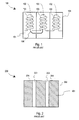
- Fig. 4 shows a longitudinal section of a filter 400 including a base plate 401, casing 402 and inner conductors 403A to 403G.
- the inner conductors 403A to 403G are customarily called resonators, even though a resonator as an electrical structure comprises an inner and outer conductor.
- the casing 402 corresponds to that of prior-art helix and coaxial filters in that it is basically shaped like a rectangular prism open at one side and additionally comprises partition walls. The outer walls of the casing and the partition walls form a compartment for each resonator.
- the base plate 401 is connected to the casing 402 such that it closes the open side of the casing.
- the base plate may be made of a printed circuit board so that at least one of its surfaces is electrically conductive or, if it is a multilayer circuit board, it has at least one electrically conductive layer.
- the electrically conductive layer in the base plate is called the ground plane.
- the ground plane is preferably located on the outer surface of the circuit board, i.e. on the bottom surface of the board with respect to the position shown in Fig. 4.
- the base plate in whole may also be made of metal or other electrically conductive material so that it constitutes a ground plane as such.
- Resonators 403A to 403G are attached to the base plate 401 such that their first end (the bottom end in Fig. 4) is in galvanic contact with the ground plane.
- a preferred method of attachment was disclosed above in conjunction with the description of the prior art, referring to Fig. 3.
- the base plate in whole is metallic, the resonators can be attached to its surface or to holes on its surface by soldering.
- the resonators are attached at the other end (the top end in Fig. 4) to the casing preferably such that the casing surface which in Fig. 4 is the top surface has a hole for each resonator and the resonators are connected to the holes by soldering or using electrically conductive glue.
- Fig. 4 shows that each resonator has a bulge, i.e. a point where the area of the cross section of the resonator suddenly increases. This is not necessary as regards the invention, but at least one resonator may be evenly thick or the area of its cross section may change in a continuous manner. Also, all resonators may be evenly thick or the areas of their cross sections may change in a continuous manner. However, it is advantageous from the manufacturing standpoint if all resonators can be made from an identical mechanical piece. In addition, Fig.
- the resonators are longer than the shortest distance between the base plate and the surface of the casing that is parallel to the base plate and that they are located at different heights with respect to the base plate such that no two adjacent resonators are at the same height with respect to the base plate.
- some of the resonators or all resonators may be as long as the shortest distance between the base plate and the surface of the casing that is parallel to the base plate and/or at least two adjacent resonators may be at the same height with respect to the base plate.
- the resonators are half-wave resonators.
- the lowest resonating frequency of such a resonator is one that corresponds to a wavelength that equals twice the electrical length of the resonator.
- the electric field maximum of an evenly thick half-wave resonator is at the middle of the resonator's longitudinal axis, and the magnetic field has maximums at both ends of the resonator.
- the locations of the maximums of the electric and magnetic fields can be varied by varying the location of the bulge with respect to the resonator ends. In a resonator where the bulge is not located at either end but somewhere in between, the electric field maximum coincides with the bulge.
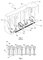
- Fig. 5 shows a longitudinal section of a filter construction 500 according to the invention with only two resonators 501 and 502.
- the figure particularly illustrates how inter-resonator electromagnetic coupling is arranged using so-called window coupling.
- a casing 503 which surrounds a filter from above and all sides has a partition wall 504 that divides it into two compartments.
- the partition wall has an upper window 505 and lower window 506 which are simply holes in the partition wall; the invention does not limit the shape, size or the location of the holes in the partition wall, but rectangular holes are the simplest to calculate and manufacture.
- a first resonator 501 has a bulge 507 located near the upper end of the resonator, and a second resonator 502 has a bulge 508 located near the lower end of the resonator.
- the electric field maximum coincides in both resonators with the bulge and is marked by o's.
- the magnetic field maximum is in both resonators near that end which is farther away from the bulge.
- the magnetic field maximum is marked by x's.
- the upper window 505 coincides with the first resonator's 501 electric field maximum and the second resonator's 502 magnetic field maximum so that the upper window provides electromagnetic coupling between the first resonator's electric field and the second resonator's magnetic field.
- the lower window 506 provides electromagnetic coupling between the first resonator's magnetic field and the second resonator's electric field.
- a coupling between an electric field and magnetic field is usually used to create a zero at a desired location in the filter's frequency response, normally below or above the pass band of a bandpass filter.
- the filter construction dimensions needed to create the desired zero can be found by experimenting. Zeros can also be created using so-called cross couplings, realized by microstrips and known in the prior art.
- Fig. 6 shows a resonator 600 according to the invention wherein an inner conductor 601 is enveloped by a casing 602.
- This can be a multiresonator filter viewed from such a direction that only one resonator can be seen, or an oscillator construction that needs only one resonator.
- the lower end of the inner conductor is attached to a base plate 603 which also closes the open side of the casing. It is known that when the temperature of the metal or other material used in the inner conductors of a resonator increases, its self-resonant frequency increases as well, which has an effect of shifting the resonant frequency of the whole resonator upwards on the frequency axis.
- the resonant frequency of a resonator according to Fig. 6 is also affected by the distance between the inner conductor and casing in such a manner that the shorter the distance the higher the resonant frequency.
- the materials of the inner conductor and casing can be selected such that the material of the inner conductor has a lower temperature coefficient of expansion than the material of the casing, so that when the temperature goes up the casing expands more than the inner conductor. The resulting increase in the distance between the inner conductor and casing has an effect of decreasing the resonant frequency.
- suitable dimensions and materials for the inner conductor and casing With suitable dimensions and materials for the inner conductor and casing, the effects of the increase of self-resonant frequency and increase of the distance between the inner conductor and casing cancel each other out, so that the resonant frequency remains nearly the same in spite of the temperature increase.
- a suitable material for the casing could be e.g. aluminium and a suitable resonator material in that case iron. Temperature compensation is also affected by the location and proportions of a possible bulge in the inner conductor. Suitable dimensions can be determined by experimenting.
- the location of the bulge in the resonator's inner conductor shown in Fig.6 is exemplary only.
- the bulge may be located at another point in the resonator.
- the resonator may also be evenly thick or its thickness may change steplessly.
- the construction according to the invention one can relatively easily produce filters and oscillators for a frequency range extending from about 2 GHz to nearly 20 GHz. As it uses half-wave resonators the construction will not be too small, thus avoiding problems related to manufacturability. On the other hand, the construction is much smaller than a waveguide construction with corresponding characteristics. The construction is very sturdy as the inner conductors of the resonators are supported at both ends. The construction has few separate parts and the parts are dimensioned so as to have few factors that would potentially cause variation in the characteristics of the products manufactured.
- the embodiments described above are naturally exemplary only and do not limit the invention.
- the invention does not limit the number of resonators in a filter.
- a minimum number required to build a working filter is usually two resonators.
- the more resonators in a filter the more accurately one can define the frequency response of the filter.
- the physical size of the filter increases and losses become greater.
- An oscillator can be realized using one resonator.
Landscapes
- Physics & Mathematics (AREA)
- Electromagnetism (AREA)
- Control Of Motors That Do Not Use Commutators (AREA)
- Inductance-Capacitance Distribution Constants And Capacitance-Resistance Oscillators (AREA)
Applications Claiming Priority (2)
| Application Number | Priority Date | Filing Date | Title |
|---|---|---|---|
| FI981026 | 1998-05-08 | ||
| FI981026A FI113579B (fi) | 1998-05-08 | 1998-05-08 | Suodatinrakenne ja oskillaatori useiden gigahertsien taajuuksille |
Publications (2)
| Publication Number | Publication Date |
|---|---|
| EP0955688A2 true EP0955688A2 (de) | 1999-11-10 |
| EP0955688A3 EP0955688A3 (de) | 2000-11-29 |
Family
ID=8551682
Family Applications (1)
| Application Number | Title | Priority Date | Filing Date |
|---|---|---|---|
| EP99660071A Withdrawn EP0955688A3 (de) | 1998-05-08 | 1999-05-05 | Filterkonstruktion und Oszillator für Frequenzen von mehreren Gigahertz |
Country Status (3)
| Country | Link |
|---|---|
| US (1) | US6215376B1 (de) |
| EP (1) | EP0955688A3 (de) |
| FI (1) | FI113579B (de) |
Cited By (1)
| Publication number | Priority date | Publication date | Assignee | Title |
|---|---|---|---|---|
| WO2006029868A1 (de) * | 2004-09-16 | 2006-03-23 | Kathrein-Austria Ges.M.B.H | Hochfrequenzfilter |
Families Citing this family (38)
| Publication number | Priority date | Publication date | Assignee | Title |
|---|---|---|---|---|
| US6806791B1 (en) * | 2000-02-29 | 2004-10-19 | Radio Frequency Systems, Inc. | Tunable microwave multiplexer |
| FI114251B (fi) * | 2000-09-22 | 2004-09-15 | Filtronic Lk Oy | Resonaattorisuodatin |
| CN1989652B (zh) | 2004-06-28 | 2013-03-13 | 脉冲芬兰有限公司 | 天线部件 |
| US7068128B1 (en) * | 2004-07-21 | 2006-06-27 | Hrl Laboratories, Llc | Compact combline resonator and filter |
| FI20055420A0 (fi) * | 2005-07-25 | 2005-07-25 | Lk Products Oy | Säädettävä monikaista antenni |
| FI119009B (fi) | 2005-10-03 | 2008-06-13 | Pulse Finland Oy | Monikaistainen antennijärjestelmä |
| FI118782B (fi) | 2005-10-14 | 2008-03-14 | Pulse Finland Oy | Säädettävä antenni |
| FI119577B (fi) * | 2005-11-24 | 2008-12-31 | Pulse Finland Oy | Monikaistainen antennikomponentti |
| US8618990B2 (en) | 2011-04-13 | 2013-12-31 | Pulse Finland Oy | Wideband antenna and methods |
| US10211538B2 (en) | 2006-12-28 | 2019-02-19 | Pulse Finland Oy | Directional antenna apparatus and methods |
| FI20075269A0 (fi) | 2007-04-19 | 2007-04-19 | Pulse Finland Oy | Menetelmä ja järjestely antennin sovittamiseksi |
| FI120427B (fi) | 2007-08-30 | 2009-10-15 | Pulse Finland Oy | Säädettävä monikaista-antenni |
| FI20096134A0 (fi) | 2009-11-03 | 2009-11-03 | Pulse Finland Oy | Säädettävä antenni |
| FI20096251A0 (sv) | 2009-11-27 | 2009-11-27 | Pulse Finland Oy | MIMO-antenn |
| US8847833B2 (en) | 2009-12-29 | 2014-09-30 | Pulse Finland Oy | Loop resonator apparatus and methods for enhanced field control |
| FI20105158A7 (fi) | 2010-02-18 | 2011-08-19 | Pulse Finland Oy | Kuorisäteilijällä varustettu antenni |
| US9406998B2 (en) | 2010-04-21 | 2016-08-02 | Pulse Finland Oy | Distributed multiband antenna and methods |
| FI20115072A0 (fi) | 2011-01-25 | 2011-01-25 | Pulse Finland Oy | Moniresonanssiantenni, -antennimoduuli ja radiolaite |
| US9673507B2 (en) | 2011-02-11 | 2017-06-06 | Pulse Finland Oy | Chassis-excited antenna apparatus and methods |
| US8648752B2 (en) | 2011-02-11 | 2014-02-11 | Pulse Finland Oy | Chassis-excited antenna apparatus and methods |
| US8866689B2 (en) | 2011-07-07 | 2014-10-21 | Pulse Finland Oy | Multi-band antenna and methods for long term evolution wireless system |
| US9450291B2 (en) | 2011-07-25 | 2016-09-20 | Pulse Finland Oy | Multiband slot loop antenna apparatus and methods |
| US9123990B2 (en) | 2011-10-07 | 2015-09-01 | Pulse Finland Oy | Multi-feed antenna apparatus and methods |
| US9531058B2 (en) | 2011-12-20 | 2016-12-27 | Pulse Finland Oy | Loosely-coupled radio antenna apparatus and methods |
| US9484619B2 (en) | 2011-12-21 | 2016-11-01 | Pulse Finland Oy | Switchable diversity antenna apparatus and methods |
| US8988296B2 (en) | 2012-04-04 | 2015-03-24 | Pulse Finland Oy | Compact polarized antenna and methods |
| US9979078B2 (en) | 2012-10-25 | 2018-05-22 | Pulse Finland Oy | Modular cell antenna apparatus and methods |
| US10069209B2 (en) | 2012-11-06 | 2018-09-04 | Pulse Finland Oy | Capacitively coupled antenna apparatus and methods |
| US9647338B2 (en) | 2013-03-11 | 2017-05-09 | Pulse Finland Oy | Coupled antenna structure and methods |
| US10079428B2 (en) | 2013-03-11 | 2018-09-18 | Pulse Finland Oy | Coupled antenna structure and methods |
| US9634383B2 (en) | 2013-06-26 | 2017-04-25 | Pulse Finland Oy | Galvanically separated non-interacting antenna sector apparatus and methods |
| US9680212B2 (en) | 2013-11-20 | 2017-06-13 | Pulse Finland Oy | Capacitive grounding methods and apparatus for mobile devices |
| US9590308B2 (en) | 2013-12-03 | 2017-03-07 | Pulse Electronics, Inc. | Reduced surface area antenna apparatus and mobile communications devices incorporating the same |
| US9350081B2 (en) | 2014-01-14 | 2016-05-24 | Pulse Finland Oy | Switchable multi-radiator high band antenna apparatus |
| US9948002B2 (en) | 2014-08-26 | 2018-04-17 | Pulse Finland Oy | Antenna apparatus with an integrated proximity sensor and methods |
| US9973228B2 (en) | 2014-08-26 | 2018-05-15 | Pulse Finland Oy | Antenna apparatus with an integrated proximity sensor and methods |
| US9722308B2 (en) | 2014-08-28 | 2017-08-01 | Pulse Finland Oy | Low passive intermodulation distributed antenna system for multiple-input multiple-output systems and methods of use |
| US9906260B2 (en) | 2015-07-30 | 2018-02-27 | Pulse Finland Oy | Sensor-based closed loop antenna swapping apparatus and methods |
Family Cites Families (15)
| Publication number | Priority date | Publication date | Assignee | Title |
|---|---|---|---|---|
| US3617954A (en) * | 1970-05-08 | 1971-11-02 | Microwave Dev Lab Inc | Semilumped comb line filter |
| GB1358980A (en) * | 1971-06-15 | 1974-07-03 | Ferranti Ltd | Microwave filters |
| US4066988A (en) * | 1976-09-07 | 1978-01-03 | Stanford Research Institute | Electromagnetic resonators having slot-located switches for tuning to different frequencies |
| DE2653856C2 (de) * | 1976-11-26 | 1978-09-28 | Siemens Ag, 1000 Berlin Und 8000 Muenchen | Filter für sehr kurze elektromagnetische Wellen |
| JPS5717201A (en) * | 1980-07-07 | 1982-01-28 | Fujitsu Ltd | Dielectric substance filter |
| US4342969A (en) * | 1980-10-06 | 1982-08-03 | General Electric Company | Means for matching impedances between a helical resonator and a circuit connected thereto |
| US5130683A (en) | 1991-04-01 | 1992-07-14 | Motorola, Inc. | Half wave resonator dielectric filter construction having self-shielding top and bottom surfaces |
| US5262742A (en) | 1992-05-20 | 1993-11-16 | Radio Frequency Systems, Inc. | Half-wave folded cross-coupled filter |
| US5557247A (en) * | 1993-08-06 | 1996-09-17 | Uab Research Foundation | Radio frequency volume coils for imaging and spectroscopy |
| JP3239552B2 (ja) | 1993-09-16 | 2001-12-17 | 株式会社村田製作所 | 誘電体共振器装置 |
| JP3282351B2 (ja) | 1994-02-17 | 2002-05-13 | 株式会社村田製作所 | 誘電体共振器装置 |
| FI98870C (fi) * | 1994-05-26 | 1997-08-25 | Lk Products Oy | Dielektrinen suodatin |
| FI97754C (fi) * | 1994-12-21 | 1997-02-10 | Verdera Oy | Resonaattorin resonanssitaajuuden sähköinen säätö |
| US5684439A (en) | 1995-10-10 | 1997-11-04 | Motorola, Inc. | Half wave ceramic filter with open circuit at both ends |
| JPH09219605A (ja) * | 1996-02-09 | 1997-08-19 | Ngk Spark Plug Co Ltd | 誘電体フィルタ及びその共振周波数調整方法 |
-
1998
- 1998-05-08 FI FI981026A patent/FI113579B/fi active
-
1999
- 1999-05-05 EP EP99660071A patent/EP0955688A3/de not_active Withdrawn
- 1999-05-07 US US09/310,706 patent/US6215376B1/en not_active Expired - Fee Related
Cited By (2)
| Publication number | Priority date | Publication date | Assignee | Title |
|---|---|---|---|---|
| WO2006029868A1 (de) * | 2004-09-16 | 2006-03-23 | Kathrein-Austria Ges.M.B.H | Hochfrequenzfilter |
| CN100578855C (zh) * | 2004-09-16 | 2010-01-06 | 凯仕林奥地利有限公司 | 高频滤波器 |
Also Published As
| Publication number | Publication date |
|---|---|
| FI113579B (fi) | 2004-05-14 |
| FI981026A0 (fi) | 1998-05-08 |
| FI981026L (fi) | 1999-11-09 |
| EP0955688A3 (de) | 2000-11-29 |
| US6215376B1 (en) | 2001-04-10 |
Similar Documents
| Publication | Publication Date | Title |
|---|---|---|
| US6215376B1 (en) | Filter construction and oscillator for frequencies of several gigahertz | |
| US4410868A (en) | Dielectric filter | |
| JP4516883B2 (ja) | 導波管とマイクロストリップ給電線との間の非接触移行部素子 | |
| US7142074B2 (en) | Multilayer waveguide filter employing via metals | |
| US7236069B2 (en) | Adjustable resonator filter | |
| CA2313925A1 (en) | Tunable bandpass filter | |
| JPH08307104A (ja) | 無線周波フィルター | |
| WO2015079227A1 (en) | Ceramic waveguide filter apparatus and method of manufacture and use thereof | |
| KR100287258B1 (ko) | 유전체공진기,유전체필터,듀플렉서및통신장치 | |
| EP0764996B1 (de) | In Resonanzfrequenz variierbarer dielektrischer Resonator | |
| EP1118134B1 (de) | Koaxialer hohlraumresonator | |
| EP3583656B1 (de) | Ein mikrowellenresonator, ein mikrowellenfilter und ein mikrowellenmultiplexer | |
| EP1079457B1 (de) | Dielektrische Resonanzvorrichtung, dielektrisches Filter, zusammengestellte dielektrische Filtervorrichtung, dielektrischer Duplexer und Kommunikationsgerät | |
| US6727784B2 (en) | Dielectric device | |
| EP0899806B1 (de) | Dielektrisches Filter, Duplexer, und Kommunikationssystem | |
| US6069543A (en) | Dielectric resonator capable of varying resonant frequency | |
| EP1777774B1 (de) | Dielektrische Anordnung | |
| EP0743696B1 (de) | Dielektrisches Filter und Verfahren zu dessen Herstellung | |
| KR100297346B1 (ko) | 유전체필터및이를이용한통신장치 | |
| EP1128461B1 (de) | Bandpassfilter und Verfahren zu seiner Herstellung | |
| KR102873802B1 (ko) | 무선통신 시스템 필터 | |
| JP2021078048A (ja) | 誘電体共振部品 | |
| JPS63214001A (ja) | 誘電体共振器濾波器 | |
| JP2002009502A (ja) | バンドパスフィルタ | |
| GB2570765A (en) | Resonator apparatus and method of use thereof |
Legal Events
| Date | Code | Title | Description |
|---|---|---|---|
| PUAI | Public reference made under article 153(3) epc to a published international application that has entered the european phase |
Free format text: ORIGINAL CODE: 0009012 |
|
| AK | Designated contracting states |
Kind code of ref document: A2 Designated state(s): DE FR GB IT |
|
| AX | Request for extension of the european patent |
Free format text: AL;LT;LV;MK;RO;SI |
|
| RAP1 | Party data changed (applicant data changed or rights of an application transferred) |
Owner name: FILTRONIC LK OY |
|
| PUAL | Search report despatched |
Free format text: ORIGINAL CODE: 0009013 |
|
| AK | Designated contracting states |
Kind code of ref document: A3 Designated state(s): AT BE CH CY DE DK ES FI FR GB GR IE IT LI LU MC NL PT SE |
|
| AX | Request for extension of the european patent |
Free format text: AL;LT;LV;MK;RO;SI |
|
| AKX | Designation fees paid |
Free format text: DE FR GB IT |
|
| 17P | Request for examination filed |
Effective date: 20010607 |
|
| R17P | Request for examination filed (corrected) |
Effective date: 20010529 |
|
| RAP1 | Party data changed (applicant data changed or rights of an application transferred) |
Owner name: FILTRONIC COMTEK OY |
|
| STAA | Information on the status of an ep patent application or granted ep patent |
Free format text: STATUS: THE APPLICATION IS DEEMED TO BE WITHDRAWN |
|
| 18D | Application deemed to be withdrawn |
Effective date: 20060321 |