EP0955709A2 - Laser bleu à émission le long d'un bord - Google Patents
Laser bleu à émission le long d'un bord Download PDFInfo
- Publication number
- EP0955709A2 EP0955709A2 EP99303312A EP99303312A EP0955709A2 EP 0955709 A2 EP0955709 A2 EP 0955709A2 EP 99303312 A EP99303312 A EP 99303312A EP 99303312 A EP99303312 A EP 99303312A EP 0955709 A2 EP0955709 A2 EP 0955709A2
- Authority
- EP
- European Patent Office
- Prior art keywords
- layer
- gan
- gallium nitride
- edge emitting
- emitting laser
- Prior art date
- Legal status (The legal status is an assumption and is not a legal conclusion. Google has not performed a legal analysis and makes no representation as to the accuracy of the status listed.)
- Withdrawn
Links
- 229910002601 GaN Inorganic materials 0.000 claims abstract description 75
- JMASRVWKEDWRBT-UHFFFAOYSA-N Gallium nitride Chemical compound [Ga]#N JMASRVWKEDWRBT-UHFFFAOYSA-N 0.000 claims abstract description 64
- 239000004065 semiconductor Substances 0.000 claims abstract description 40
- 239000000758 substrate Substances 0.000 claims abstract description 17
- 229910052594 sapphire Inorganic materials 0.000 claims abstract description 8
- 239000010980 sapphire Substances 0.000 claims abstract description 8
- 229910045601 alloy Inorganic materials 0.000 claims description 5
- 239000000956 alloy Substances 0.000 claims description 5
- 239000003989 dielectric material Substances 0.000 claims description 5
- 229910052782 aluminium Inorganic materials 0.000 claims description 3
- XAGFODPZIPBFFR-UHFFFAOYSA-N aluminium Chemical compound [Al] XAGFODPZIPBFFR-UHFFFAOYSA-N 0.000 claims description 3
- 230000001427 coherent effect Effects 0.000 claims description 3
- 229910052738 indium Inorganic materials 0.000 claims description 3
- APFVFJFRJDLVQX-UHFFFAOYSA-N indium atom Chemical compound [In] APFVFJFRJDLVQX-UHFFFAOYSA-N 0.000 claims description 3
- 230000007547 defect Effects 0.000 abstract description 12
- 238000000407 epitaxy Methods 0.000 abstract description 4
- 208000012868 Overgrowth Diseases 0.000 abstract description 3
- 238000000059 patterning Methods 0.000 abstract description 2
- VYPSYNLAJGMNEJ-UHFFFAOYSA-N Silicium dioxide Chemical compound O=[Si]=O VYPSYNLAJGMNEJ-UHFFFAOYSA-N 0.000 description 14
- 238000005253 cladding Methods 0.000 description 10
- 239000000377 silicon dioxide Substances 0.000 description 7
- KRHYYFGTRYWZRS-UHFFFAOYSA-N Fluorane Chemical compound F KRHYYFGTRYWZRS-UHFFFAOYSA-N 0.000 description 6
- 238000005530 etching Methods 0.000 description 5
- 229910018885 Pt—Au Inorganic materials 0.000 description 4
- RNQKDQAVIXDKAG-UHFFFAOYSA-N aluminum gallium Chemical compound [Al].[Ga] RNQKDQAVIXDKAG-UHFFFAOYSA-N 0.000 description 4
- 239000013078 crystal Substances 0.000 description 4
- 229910052737 gold Inorganic materials 0.000 description 4
- 238000000034 method Methods 0.000 description 4
- 238000000623 plasma-assisted chemical vapour deposition Methods 0.000 description 4
- FYYHWMGAXLPEAU-UHFFFAOYSA-N Magnesium Chemical compound [Mg] FYYHWMGAXLPEAU-UHFFFAOYSA-N 0.000 description 3
- 229910052749 magnesium Inorganic materials 0.000 description 3
- 239000011777 magnesium Substances 0.000 description 3
- 239000000463 material Substances 0.000 description 3
- 238000001883 metal evaporation Methods 0.000 description 3
- TWNQGVIAIRXVLR-UHFFFAOYSA-N oxo(oxoalumanyloxy)alumane Chemical group O=[Al]O[Al]=O TWNQGVIAIRXVLR-UHFFFAOYSA-N 0.000 description 3
- QGZKDVFQNNGYKY-UHFFFAOYSA-N Ammonia Chemical compound N QGZKDVFQNNGYKY-UHFFFAOYSA-N 0.000 description 2
- 229910004205 SiNX Inorganic materials 0.000 description 2
- XUIMIQQOPSSXEZ-UHFFFAOYSA-N Silicon Chemical compound [Si] XUIMIQQOPSSXEZ-UHFFFAOYSA-N 0.000 description 2
- 238000005229 chemical vapour deposition Methods 0.000 description 2
- 238000005137 deposition process Methods 0.000 description 2
- 238000005566 electron beam evaporation Methods 0.000 description 2
- 230000000873 masking effect Effects 0.000 description 2
- 238000002488 metal-organic chemical vapour deposition Methods 0.000 description 2
- QPJSUIGXIBEQAC-UHFFFAOYSA-N n-(2,4-dichloro-5-propan-2-yloxyphenyl)acetamide Chemical compound CC(C)OC1=CC(NC(C)=O)=C(Cl)C=C1Cl QPJSUIGXIBEQAC-UHFFFAOYSA-N 0.000 description 2
- 230000003287 optical effect Effects 0.000 description 2
- 229910052710 silicon Inorganic materials 0.000 description 2
- 239000010703 silicon Substances 0.000 description 2
- 235000012239 silicon dioxide Nutrition 0.000 description 2
- 229910052814 silicon oxide Inorganic materials 0.000 description 2
- 229910052581 Si3N4 Inorganic materials 0.000 description 1
- 229910021529 ammonia Inorganic materials 0.000 description 1
- 230000015572 biosynthetic process Effects 0.000 description 1
- 238000000151 deposition Methods 0.000 description 1
- 230000008021 deposition Effects 0.000 description 1
- 238000001312 dry etching Methods 0.000 description 1
- 238000002513 implantation Methods 0.000 description 1
- 238000007648 laser printing Methods 0.000 description 1
- 238000004519 manufacturing process Methods 0.000 description 1
- 229910052751 metal Inorganic materials 0.000 description 1
- 239000002184 metal Substances 0.000 description 1
- 238000001465 metallisation Methods 0.000 description 1
- 150000004767 nitrides Chemical class 0.000 description 1
- 239000013307 optical fiber Substances 0.000 description 1
- 125000002524 organometallic group Chemical group 0.000 description 1
- 229920002120 photoresistant polymer Polymers 0.000 description 1
- 238000001020 plasma etching Methods 0.000 description 1
- HQVNEWCFYHHQES-UHFFFAOYSA-N silicon nitride Chemical compound N12[Si]34N5[Si]62N3[Si]51N64 HQVNEWCFYHHQES-UHFFFAOYSA-N 0.000 description 1
- -1 silicon oxide nitride Chemical class 0.000 description 1
- 239000007787 solid Substances 0.000 description 1
- 125000006850 spacer group Chemical group 0.000 description 1
- 238000000927 vapour-phase epitaxy Methods 0.000 description 1
Images



Classifications
-
- B—PERFORMING OPERATIONS; TRANSPORTING
- B82—NANOTECHNOLOGY
- B82Y—SPECIFIC USES OR APPLICATIONS OF NANOSTRUCTURES; MEASUREMENT OR ANALYSIS OF NANOSTRUCTURES; MANUFACTURE OR TREATMENT OF NANOSTRUCTURES
- B82Y20/00—Nanooptics, e.g. quantum optics or photonic crystals
-
- H—ELECTRICITY
- H01—ELECTRIC ELEMENTS
- H01S—DEVICES USING THE PROCESS OF LIGHT AMPLIFICATION BY STIMULATED EMISSION OF RADIATION [LASER] TO AMPLIFY OR GENERATE LIGHT; DEVICES USING STIMULATED EMISSION OF ELECTROMAGNETIC RADIATION IN WAVE RANGES OTHER THAN OPTICAL
- H01S5/00—Semiconductor lasers
- H01S5/04—Processes or apparatus for excitation, e.g. pumping, e.g. by electron beams
- H01S5/042—Electrical excitation ; Circuits therefor
- H01S5/0425—Electrodes, e.g. characterised by the structure
- H01S5/04254—Electrodes, e.g. characterised by the structure characterised by the shape
-
- H—ELECTRICITY
- H01—ELECTRIC ELEMENTS
- H01S—DEVICES USING THE PROCESS OF LIGHT AMPLIFICATION BY STIMULATED EMISSION OF RADIATION [LASER] TO AMPLIFY OR GENERATE LIGHT; DEVICES USING STIMULATED EMISSION OF ELECTROMAGNETIC RADIATION IN WAVE RANGES OTHER THAN OPTICAL
- H01S5/00—Semiconductor lasers
- H01S5/30—Structure or shape of the active region; Materials used for the active region
- H01S5/34—Structure or shape of the active region; Materials used for the active region comprising quantum well or superlattice structures, e.g. single quantum well [SQW] lasers, multiple quantum well [MQW] lasers or graded index separate confinement heterostructure [GRINSCH] lasers
- H01S5/343—Structure or shape of the active region; Materials used for the active region comprising quantum well or superlattice structures, e.g. single quantum well [SQW] lasers, multiple quantum well [MQW] lasers or graded index separate confinement heterostructure [GRINSCH] lasers in AIIIBV compounds, e.g. AlGaAs-laser, InP-based laser
- H01S5/34333—Structure or shape of the active region; Materials used for the active region comprising quantum well or superlattice structures, e.g. single quantum well [SQW] lasers, multiple quantum well [MQW] lasers or graded index separate confinement heterostructure [GRINSCH] lasers in AIIIBV compounds, e.g. AlGaAs-laser, InP-based laser with a well layer based on Ga(In)N or Ga(In)P, e.g. blue laser
-
- H—ELECTRICITY
- H01—ELECTRIC ELEMENTS
- H01S—DEVICES USING THE PROCESS OF LIGHT AMPLIFICATION BY STIMULATED EMISSION OF RADIATION [LASER] TO AMPLIFY OR GENERATE LIGHT; DEVICES USING STIMULATED EMISSION OF ELECTROMAGNETIC RADIATION IN WAVE RANGES OTHER THAN OPTICAL
- H01S5/00—Semiconductor lasers
- H01S5/02—Structural details or components not essential to laser action
- H01S5/0206—Substrates, e.g. growth, shape, material, removal or bonding
- H01S5/0213—Sapphire, quartz or diamond based substrates
-
- H—ELECTRICITY
- H01—ELECTRIC ELEMENTS
- H01S—DEVICES USING THE PROCESS OF LIGHT AMPLIFICATION BY STIMULATED EMISSION OF RADIATION [LASER] TO AMPLIFY OR GENERATE LIGHT; DEVICES USING STIMULATED EMISSION OF ELECTROMAGNETIC RADIATION IN WAVE RANGES OTHER THAN OPTICAL
- H01S5/00—Semiconductor lasers
- H01S5/04—Processes or apparatus for excitation, e.g. pumping, e.g. by electron beams
- H01S5/042—Electrical excitation ; Circuits therefor
- H01S5/0425—Electrodes, e.g. characterised by the structure
- H01S5/04256—Electrodes, e.g. characterised by the structure characterised by the configuration
- H01S5/04257—Electrodes, e.g. characterised by the structure characterised by the configuration having positive and negative electrodes on the same side of the substrate
-
- H—ELECTRICITY
- H01—ELECTRIC ELEMENTS
- H01S—DEVICES USING THE PROCESS OF LIGHT AMPLIFICATION BY STIMULATED EMISSION OF RADIATION [LASER] TO AMPLIFY OR GENERATE LIGHT; DEVICES USING STIMULATED EMISSION OF ELECTROMAGNETIC RADIATION IN WAVE RANGES OTHER THAN OPTICAL
- H01S5/00—Semiconductor lasers
- H01S5/20—Structure or shape of the semiconductor body to guide the optical wave ; Confining structures perpendicular to the optical axis, e.g. index or gain guiding, stripe geometry, broad area lasers, gain tailoring, transverse or lateral reflectors, special cladding structures, MQW barrier reflection layers
- H01S5/22—Structure or shape of the semiconductor body to guide the optical wave ; Confining structures perpendicular to the optical axis, e.g. index or gain guiding, stripe geometry, broad area lasers, gain tailoring, transverse or lateral reflectors, special cladding structures, MQW barrier reflection layers having a ridge or stripe structure
Definitions
- This invention relates to a monolithic semiconductor laser structure and, more particularly, to an independently addressable, edge emitting laser in the blue wavelength range.
- Monolithic solid state semiconductor lasers are very desirable light sources for high speed laser printing, optical fiber communications and other applications.
- Edge emitting lasers are currently used in the vast majority of applications.
- a common laser structure is a so-called “edge emitting laser” where light is emitted from the edge of a monolithic structure of semiconductor layers.
- Edge emitting lasers typically produce a beam with a large power output than surface emitting lasers.
- Prior art quantum well edge emitting lasers can emit light in the wavelength range of about 600 to 650 nanometers (the red range) or in the range above 650 nanometers (the infrared range) . However, there are important applications for laser devices that emit light in the wavelength range around 400 nanometers (the blue range).
- GaN gallium nitride and its alloys with indium and aluminum are used as the semiconductor layers in the blue laser structure.
- GaN itself cannot be used as a practical substrate.
- the problem is the lack of a suitable, lattice-matched substrate for the GaN semiconductor layers. Without a substrate with a lattice constant close to that of GaN, there will be a high density of extended defects in the nitride layers.
- An active layer of GaN and its alloys on a poorly lattice matched substrate will emit coherent blue light poorly and inefficiently, if at all.
- Sapphire Al 2 O 3
- GaN gallium-nitride
- An approximate epitaxial relationship between a sapphire substrate and a GaN alloy semiconductor laser structure can be obtained by matching specific crystallographic directions. However, a lattice mismatch of approximately 15 percent results from such a semiconductor structure.
- the present invention provides an independently addressable, edge emitting laser in the blue wavelength range of 390 to 430 nanometers.
- the gallium nitride-based laser structure is grown by selective area epitaxy and lateral mask overgrowth. By appropriate patterning of a dielectric mask on the gallium nitride layer on a sapphire substrate, areas in a second gallium nitride layer can have a low defect density upon which the remainder of the laser structure can be formed.
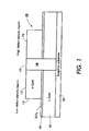
- Figure 1 illustrates a gallium nitride (GaN) crystal structure 100 for use in a vertical cavity surface emitting laser in accordance with the present invention.
- GaN gallium nitride
- the structure 100 comprises a sapphire (Al 2 O 3 ) substrate 102 upon which is first grown a n-gallium nitride (n-GaN) base layer 104 using an epitaxial deposition process known as metal-organic chemical vapor deposition (“MOCVD”) as is well known in the art.
- MOCVD metal-organic chemical vapor deposition
- a 200 nm thick dielectric film 106 of silicon dioxide (SiO 2 ) is then deposited on the GaN base layer 104 by plasma-enhanced chemical vapor deposition ("PECVD") or by electron beam evaporation.
- PECVD plasma-enhanced chemical vapor deposition
- the dielectric film 106 is then patterned by using standard photolithographic procedures and etching with hydrofluoric acid (HF).
- a thin linear stripe 108 is etched down in the dielectric film 106 to expose the surface of the GaN base layer 104.
- a second n-gallium nitride (n-GaN) layer 110 of 4 ⁇ m thickness with a lateral width of 16 ⁇ m is then grown laterally starting at the thin exposed stripe 108.
- the GaN layer 110 grows laterally above the dielectric film 106 under high temperature and high ammonia flow, as described in Kapolnek et al., "Anistropic epitaxial lateral growth in GaN selective area epitaxy", Applied Physics Letters, vol. 71(9), 1 September 1997, pp. 1204-1206.
- the layer 110 starts selectively only in the exposed GaN area 108, but not on the top surface of the SiO 2 layer 106. As the layer 110 gets thicker, the layer starts to laterally overgrow the SiO 2 layer 106. Since this laterally overgrown material is attached to the lower GaN layer 104 only on one side, it will grow without strain and, therefore, without dislocations. The second GaN layer 110 will be laterally overgrown over the GaN base layer 104 and above the dielectric film 106 on each side of the stripe 108.
- the GaN layer 110 consists of three sections: a first or end section 112 atop one portion of the dielectric film 106, a second or middle section 114 atop the exposed stripe 108 of the GaN base layer 104 and a third or end section 116 atop another portion of the dielectric film 106.
- the two end portions 112 and 116 since they are deposited on top of the dielectric film 106 are in the low defect density regions of the GaN layer 110.
- the middle section 114 since it is deposited on the other first GaN base layer 104 is in the high defect density regions of the second GaN layer 110.
- the laser heterostructures will be grown by epitaxy upon one section of the lateral overgrowth of the GaN layer 110 upon the dielectric film 106 and the linear stripe 108 of the GaN base layer 104.
- the subsequent growth of GaN based laser heterostructures over a patterned substrate 110 leads to low defect crystal areas 112 and 116 away from the high defect crystal area 114.
- the dielectric film 106 deposited on the GaN base layer 104 can, in the alternative, be silicon nitride (SiN x ) or silicon oxide nitride (SiON).
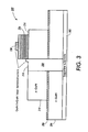
- the blue edge emitting laser semiconductor structure 200 of Figure 2 is fabricated in accordance to the present invention.
- the blue edge emitting laser structure 200 comprises a sapphire (Al 2 O 3 ) substrate 202 upon which is first grown a n-gallium nitride (n-GaN) base layer 204 using an epitaxial deposition process known as metal-organic chemical vapor deposition (“MOCVD”) as is well known in the art.
- MOCVD metal-organic chemical vapor deposition
- a 200 nm thick dielectric film 206 of silicon dioxide (SiO 2 ) is then deposited on the GaN base layer 204 by plasma-enhanced chemical vapor deposition ("PECVD") or by electron beam evaporation.
- PECVD plasma-enhanced chemical vapor deposition
- the dielectric film 206 is then patterned by using standard photolithographic procedures and etching with hydrofluoric acid (HF).
- a thin linear stripe 208 is etched down in the dielectric film 206 to expose the surface of the GaN base layer 204.
- a second n-gallium nitride (n-GaN) layer 210 of 4 ⁇ m thickness with a lateral width of 16 ⁇ m is then selectively deposited on the dielectric film 206 and the thin exposed stripe 208 of the GaN base layer 204.
- the second GaN layer 210 will be laterally overgrown over the GaN base layer 204 and above the dielectric film 206 on each side of the stripe 208.
- the GaN layer 210 consists of three sections: a first or end section 212 atop one portion of the dielectric film 206, a second or middle section 214 atop the exposed stripe 208 of the GaN base layer 204 and a third or end section 216 atop another portion of the dielectric film 206.
- the two end portions 212 and 216 since they are deposited on top of the dielectric film 206 are in the low defect density regions of the GaN layer 210.
- the middle section 214 since it is deposited on the GaN base layer 204 is in the high defect density regions of the second GaN layer 210.
- the laser heterostructure is then deposited on the GaN layer 210.
- n-Al 0.08 Ga 0.92 N aluminum gallium nitride cladding layer 218 is deposited on the GaN layer 210.
- the n-Al 0.08 Ga 0.92 N aluminum gallium nitride cladding layer 218 has a thickness of 0.5 ⁇ m and is silicon doped to a concentration of 5 x 10 17 cm -3 .
- a first lower n-GaN confinement layer 220 is deposited upon the lower cladding layer 218.
- the n-GaN confinement layer 220 has a thickness of 100 nm and is silicon doped to a concentration of 10 18 cm -3 .
- An In 0.15 Ga 0.85 N/GaN multiple quantum well active layer 222 is deposited on the confinement layer 220.
- the In 0.15 Ga 0.85 N/GaN multiple quantum well active layer 222 is undoped and has a thickness of 120 nm.
- a second upper p-GaN confinement layer 224 is deposited upon the multiple quantum well active layer 222.
- the p-GaN confinement layer 224 has a thickness of 100 nm and is magnesium doped to a concentration of 10 18 cm -3 .
- An upper p-Al 0.08 Ga 0.92 N aluminum gallium nitride cladding layer 226 is deposited on the confinement layer 224.
- the p-Al 0.08 Ga 0.92 N aluminum gallium nitride cladding layer 226 has a thickness of 0.5 ⁇ m and is magnesium doped to a concentration of 5 x 10 17 cm -3 .
- a third p-GaN contact layer 228 is deposited on the upper cladding layer 226.
- the contact layer 228 has a thickness of 120 nanometers and is magnesium doped to a concentration of 5 x 10 17 cm -3 .
- the multiple quantum well layer 222 forms the active region for emission of light in the blue wavelengths of 390 to 430 nanometers.
- the laser heterostructure 200 is formed of gallium nitride semiconductor layers and its alloys with aluminum and/or indium.
- the three sections of the second GaN layer 210 extend up through the rest of subsequently deposited semiconductor layers of the laser structure 200.
- the laser structure 200 has semiconductor layers deposited in the first or end section 230 from the first section 212 of the GaN layer 210 atop one portion of the dielectric film 206 and the third or end section 234 from the third section 216 of the GaN layer 210 atop another portion of the dielectric film 206.
- the two end portions 230 and 234 since they are deposited on top of the low defect density regions of GaN layer 210 are in the low defect density regions of the laser structure 200.
- the middle section 232 from the middle section 214 of the GaN layer 210 since it is deposited on the GaN base layer 204 is in the high defect density regions of the laser structure 200.
- a dielectric masking layer (not shown) such as a photoresist, is pattern masked on the surface of the layer 228 and the unmasked portion of the laser structure 200 is etched away down the second N-GaN layer 210 to form a ridge waveguide 236.
- the pattern masking and dry etching or reactive ion etching are techniques common to semiconductor structure manufacture and known in the art.
- the ridge waveguide 236 portion of the laser structure 200 extends above the third or end section 216 of the GaN layer 210 after etching.
- the ridge waveguide 236 forms the lateral optical confinement structure for the semiconductor laser 200 and thus the ridge precisely defines the origin of the edge emission of light from the semiconductor laser.
- the ridge waveguide is typically a small ridge of semiconductor material with a generally flat upper surface and sloped sidewalls on top of the active semiconductor layer in a semiconductor laser structure.
- One method of forming the ridge waveguide is to etch away a portion of the upper cladding layer 226 (and contact layer 230) of the epitaxially deposited semiconductor layers of the laser structure, leaving a narrow ridge 238 of the cladding layer material to define the lateral ridge waveguide.
- the particular geometry of the ridge depends upon the etching means.
- an insulating layer 240 of dielectric materials such as SiN x , SiO 2 or SiON x , is deposited on the sidewalls 242 and 244 of the ridge waveguide 236 of the laser structure.
- the insulating layer will also cover a portion of the surface of the contact layer 228.
- a p-contact 246 of Cr-Au or Ti-Pt-Au is formed by metal evaporation on the uninsulated surface of the spacer layer 230.
- an InGaN contact layer (not shown) can be deposited on the contact layer 228 first, followed by the formation of the p-contact 246.
- a n-contact 248 of Cr-Au or Ti-Pt-Au is formed by metal evaporation on the first or end section 212 of the GaN layer 210.
- an air-bridge 250 of Cr-Au or Ti-Pt-Au connects the p-contact 246 to a much larger contact pad 252 on the surface of the sapphire substrate 202.
- an air-bridge 254 of Cr-Au or Ti-Pt-Au connects the n-contact 248 to a much larger contact pad 256 on the surface of the sapphire substrate 202.
- the active region will emit light through the edge of the laser structure 200.
- the conventional reflecting facets forming the optical cavity with and perpendicular to the quantum well active layer 222 at opposite ends of the laser structure 200.
- an insulating dielectric and conformational metallization can be used to connect large contacts on the substrate to the smaller contacts on the laser structure.
- proton implantation or conformal metal evaporation may be used for the contacts.
Landscapes
- Physics & Mathematics (AREA)
- Optics & Photonics (AREA)
- Engineering & Computer Science (AREA)
- Nanotechnology (AREA)
- Chemical & Material Sciences (AREA)
- Condensed Matter Physics & Semiconductors (AREA)
- General Physics & Mathematics (AREA)
- Electromagnetism (AREA)
- Biophysics (AREA)
- Crystallography & Structural Chemistry (AREA)
- Life Sciences & Earth Sciences (AREA)
- Semiconductor Lasers (AREA)
- Led Devices (AREA)
Applications Claiming Priority (2)
| Application Number | Priority Date | Filing Date | Title |
|---|---|---|---|
| US7372198A | 1998-05-06 | 1998-05-06 | |
| US73721 | 1998-05-06 |
Publications (2)
| Publication Number | Publication Date |
|---|---|
| EP0955709A2 true EP0955709A2 (fr) | 1999-11-10 |
| EP0955709A3 EP0955709A3 (fr) | 2000-07-05 |
Family
ID=22115398
Family Applications (1)
| Application Number | Title | Priority Date | Filing Date |
|---|---|---|---|
| EP99303312A Withdrawn EP0955709A3 (fr) | 1998-05-06 | 1999-04-28 | Laser bleu à émission le long d'un bord |
Country Status (2)
| Country | Link |
|---|---|
| EP (1) | EP0955709A3 (fr) |
| JP (1) | JPH11340584A (fr) |
Cited By (1)
| Publication number | Priority date | Publication date | Assignee | Title |
|---|---|---|---|---|
| US6610144B2 (en) * | 2000-07-21 | 2003-08-26 | The Regents Of The University Of California | Method to reduce the dislocation density in group III-nitride films |
Families Citing this family (2)
| Publication number | Priority date | Publication date | Assignee | Title |
|---|---|---|---|---|
| US20030087447A1 (en) | 2001-11-08 | 2003-05-08 | Blouin Matthew R | Sample well strip |
| CN105406358B (zh) * | 2015-11-25 | 2018-11-02 | 武汉电信器件有限公司 | 一种GaN基激光器制备方法和结构 |
-
1999
- 1999-04-28 EP EP99303312A patent/EP0955709A3/fr not_active Withdrawn
- 1999-04-30 JP JP12520299A patent/JPH11340584A/ja not_active Withdrawn
Non-Patent Citations (3)
| Title |
|---|
| NAKAMURA S ET AL: "INGAN/GAN/ALGAN-BASED LASER DIODES WITH MODULATION-DOPED STRAINED- LAYER SUPERLATTICES GROWN ON AN EPITAXIALLY LATERALLY OVERGROWN GAN SUBSTRATE" APPLIED PHYSICS LETTERS,US,AMERICAN INSTITUTE OF PHYSICS. NEW YORK, vol. 72, no. 2, 12 January 1998 (1998-01-12), pages 211-213, XP000735444 ISSN: 0003-6951 * |
| NAKAMURA S: "INGAN-BASED BLUE LASER DIODES" IEEE JOURNAL OF SELECTED TOPICS IN QUANTUM ELECTRONICS,US,IEEE SERVICE CENTER, vol. 3, no. 3, 1 June 1997 (1997-06-01), pages 712-718, XP000727336 ISSN: 1077-260X * |
| SHUJI NAKAMURA ET AL: "RIDGE-GEOMETRY INGAN MULTI-QUANTUM-WELL-STRUCTURE LASER DIODES" APPLIED PHYSICS LETTERS,US,AMERICAN INSTITUTE OF PHYSICS. NEW YORK, vol. 69, no. 10, 2 September 1996 (1996-09-02), pages 1477-1479, XP000629154 ISSN: 0003-6951 * |
Cited By (1)
| Publication number | Priority date | Publication date | Assignee | Title |
|---|---|---|---|---|
| US6610144B2 (en) * | 2000-07-21 | 2003-08-26 | The Regents Of The University Of California | Method to reduce the dislocation density in group III-nitride films |
Also Published As
| Publication number | Publication date |
|---|---|
| EP0955709A3 (fr) | 2000-07-05 |
| JPH11340584A (ja) | 1999-12-10 |
Similar Documents
| Publication | Publication Date | Title |
|---|---|---|
| US6160833A (en) | Blue vertical cavity surface emitting laser | |
| US6849875B2 (en) | Nitride semiconductor device | |
| JP4352473B2 (ja) | 半導体装置の製造方法 | |
| KR100917260B1 (ko) | 결정막, 결정기판 및 반도체장치 | |
| US7781796B2 (en) | Nitride semiconductor laser element | |
| US7456039B1 (en) | Method for manufacturing semiconductor optical device | |
| KR100539289B1 (ko) | 반도체 발광 장치 및 그 제조 방법 | |
| US20040061119A1 (en) | Nitride-based semiconductor light-emitting device | |
| US6620641B2 (en) | Semiconductor light emitting device and its manufacturing method | |
| US5970080A (en) | Gallium nitride compound semiconductor light emitting element and method for fabricating the same | |
| US20030052326A1 (en) | Semiconductor light-emitting device and method for fabricating the same | |
| JP3796060B2 (ja) | 半導体レーザ素子およびその製造方法 | |
| US8183649B2 (en) | Buried aperture nitride light-emitting device | |
| EP0982819B1 (fr) | Formation par épitaxie des facettes des diodes laser en materiaux III-V | |
| JP2000022282A (ja) | 面発光型発光素子及びその製造方法 | |
| KR20000035669A (ko) | 반도체 레이저, 반도체 장치 및 이들의 제조 방법 | |
| KR20000077066A (ko) | 반도체 레이저, 그 제조 방법, 반도체 장치 및 그 제조 방법 | |
| JPH11340584A (ja) | エッジ型青色発光レ―ザ | |
| JP4415440B2 (ja) | 半導体レーザの製造方法 | |
| JENNINGS &EVERY | Office europeen des brevets EP 0 9 5 5 7 0 9 A 2 | |
| EP1026799B1 (fr) | Laser à semi-conducteur et son procédé de fabrication | |
| JPH11274641A (ja) | 半導体素子およびその製造方法 | |
| JP2002359431A (ja) | 窒化物系半導体レーザ素子及びその作製方法 | |
| JPH07176830A (ja) | 半導体発光素子の製造方法 | |
| KR100390441B1 (ko) | 수직 활성층을 가지는 청색 반도체 레이저 제조 방법 |
Legal Events
| Date | Code | Title | Description |
|---|---|---|---|
| PUAI | Public reference made under article 153(3) epc to a published international application that has entered the european phase |
Free format text: ORIGINAL CODE: 0009012 |
|
| AK | Designated contracting states |
Kind code of ref document: A2 Designated state(s): DE FR GB |
|
| AX | Request for extension of the european patent |
Free format text: AL;LT;LV;MK;RO;SI |
|
| PUAL | Search report despatched |
Free format text: ORIGINAL CODE: 0009013 |
|
| AK | Designated contracting states |
Kind code of ref document: A3 Designated state(s): AT BE CH CY DE DK ES FI FR GB GR IE IT LI LU MC NL PT SE |
|
| AX | Request for extension of the european patent |
Free format text: AL;LT;LV;MK;RO;SI |
|
| 17P | Request for examination filed |
Effective date: 20010105 |
|
| AKX | Designation fees paid |
Free format text: DE FR GB |
|
| STAA | Information on the status of an ep patent application or granted ep patent |
Free format text: STATUS: THE APPLICATION HAS BEEN WITHDRAWN |
|
| 18W | Application withdrawn |
Withdrawal date: 20010716 |