EP0955726A1 - Appareil a ondes acoustiques de surface - Google Patents
Appareil a ondes acoustiques de surface Download PDFInfo
- Publication number
- EP0955726A1 EP0955726A1 EP98928609A EP98928609A EP0955726A1 EP 0955726 A1 EP0955726 A1 EP 0955726A1 EP 98928609 A EP98928609 A EP 98928609A EP 98928609 A EP98928609 A EP 98928609A EP 0955726 A1 EP0955726 A1 EP 0955726A1
- Authority
- EP
- European Patent Office
- Prior art keywords
- surface acoustic
- acoustic wave
- substrate
- frequency
- propagation
- Prior art date
- Legal status (The legal status is an assumption and is not a legal conclusion. Google has not performed a legal analysis and makes no representation as to the accuracy of the status listed.)
- Granted
Links
- 238000010897 surface acoustic wave method Methods 0.000 title claims abstract description 70
- 239000000758 substrate Substances 0.000 claims abstract description 58
- 239000013078 crystal Substances 0.000 claims abstract description 40
- 239000000126 substance Substances 0.000 claims abstract description 5
- 230000008878 coupling Effects 0.000 description 9
- 238000010168 coupling process Methods 0.000 description 9
- 238000005859 coupling reaction Methods 0.000 description 9
- 239000010453 quartz Substances 0.000 description 9
- VYPSYNLAJGMNEJ-UHFFFAOYSA-N silicon dioxide Inorganic materials O=[Si]=O VYPSYNLAJGMNEJ-UHFFFAOYSA-N 0.000 description 9
- 238000000034 method Methods 0.000 description 6
- 238000010295 mobile communication Methods 0.000 description 5
- 230000008569 process Effects 0.000 description 5
- 230000001413 cellular effect Effects 0.000 description 4
- 238000005549 size reduction Methods 0.000 description 3
- 229910003327 LiNbO3 Inorganic materials 0.000 description 2
- 229910012463 LiTaO3 Inorganic materials 0.000 description 2
- 238000002441 X-ray diffraction Methods 0.000 description 2
- 230000008859 change Effects 0.000 description 2
- 230000000694 effects Effects 0.000 description 2
- 239000000203 mixture Substances 0.000 description 2
- 230000001902 propagating effect Effects 0.000 description 2
- 238000007738 vacuum evaporation Methods 0.000 description 2
- 208000016261 weight loss Diseases 0.000 description 2
- IRLPACMLTUPBCL-KQYNXXCUSA-N 5'-adenylyl sulfate Chemical compound C1=NC=2C(N)=NC=NC=2N1[C@@H]1O[C@H](COP(O)(=O)OS(O)(=O)=O)[C@@H](O)[C@H]1O IRLPACMLTUPBCL-KQYNXXCUSA-N 0.000 description 1
- 229910000838 Al alloy Inorganic materials 0.000 description 1
- 229910052779 Neodymium Inorganic materials 0.000 description 1
- 229910045601 alloy Inorganic materials 0.000 description 1
- 229910052782 aluminium Inorganic materials 0.000 description 1
- 229910052791 calcium Inorganic materials 0.000 description 1
- 238000004891 communication Methods 0.000 description 1
- 238000002474 experimental method Methods 0.000 description 1
- 230000002349 favourable effect Effects 0.000 description 1
- 239000012535 impurity Substances 0.000 description 1
- 238000011835 investigation Methods 0.000 description 1
- 125000004430 oxygen atom Chemical group O* 0.000 description 1
- 229910052697 platinum Inorganic materials 0.000 description 1
- 229910052710 silicon Inorganic materials 0.000 description 1
- 238000004544 sputter deposition Methods 0.000 description 1
- 230000007704 transition Effects 0.000 description 1
- 230000007306 turnover Effects 0.000 description 1
- 229910052720 vanadium Inorganic materials 0.000 description 1
- 229910052726 zirconium Inorganic materials 0.000 description 1
Images



Classifications
-
- H—ELECTRICITY
- H03—ELECTRONIC CIRCUITRY
- H03H—IMPEDANCE NETWORKS, e.g. RESONANT CIRCUITS; RESONATORS
- H03H9/00—Networks comprising electromechanical or electro-acoustic elements; Electromechanical resonators
- H03H9/02—Details
- H03H9/02535—Details of surface acoustic wave devices
- H03H9/02543—Characteristics of substrate, e.g. cutting angles
- H03H9/0259—Characteristics of substrate, e.g. cutting angles of langasite substrates
Definitions
- the present invention relates to a surface acoustic wave device comprising an interdigital electrode on a single crystal substrate.
- a surface acoustic wave device has on the surface of a piezoelectric substrate an interdigital electrode for exciting, receiving, reflecting, and propagating surface acoustic waves.
- SAW velocity surface wave velocity of surface acoustic waves
- TCF temperature coefficient of frequency
- k 2 electromechanical coupling factor
- 64LN and 36LT have an SAW velocity of 4,000 m/s or higher, and so are suitable to construct filters for high-frequency parts of terminal equipment.
- various systems are practically employed for mobile communications represented by cellular telephones all over the world, and are all used at frequencies of the order of 1 GHz.
- filters used for high-frequency parts of terminal equipment have a center frequency of approximately 1 GHz.
- Surface acoustic wave filters have a center frequency substantially proportional to the SAW velocities of piezoelectric substrates used and almost inversely proportional to the widths of electrode fingers formed on the substrates.
- a frequency band of 70 to 300 MHz is used as an intermediate frequency for mobile terminal equipment.
- a filter having a center frequency in this frequency band is constructed with the use of a surface acoustic wave device, the use of the aforesaid 64LN or 36LT as a piezoelectric substrate causes the widths of electrode fingers formed on the substrate to be much larger than those of the aforesaid filter used for a high-frequency part.
- d represent the width of an electrode finger of a surface acoustic wave transducer that forms a surface acoustic wave filter
- f 0 indicate the center frequency of the surface acoustic wave filter
- V denote the SAW velocity of the piezoelectric substrate used.
- a large electrode finger width implies that a surface acoustic wave device itself becomes large.
- a piezoelectric substrate having a low SAW velocity V it is necessary to use a piezoelectric substrate having a low SAW velocity V, as can be appreciated from equation (1).
- BGO piezoelectric substrates known to have a very low SAW velocity
- BGO piezoelectric substrate has an SAW velocity of 1,681 m/s.
- the BGO piezoelectric substrate is unsuitable to construct an intermediate-frequency filter for extracting one channel signal alone, because its temperature coefficient of frequency or its TCF is as large as -122 ppm/°C. This is because a large TCF value implies that the center frequency of the surface acoustic wave filter varies largely with temperature.
- large TCF is unsuitable for an intermediate-frequency filter because undesired signals may possibly be extracted from other channel adjacent to the desired channel.
- ST quartz crystal such as one referred to in Table 1.
- the ST quartz crystal is suitable to construct an intermediate-frequency filter because its temperature coefficient of frequency or its TCF is almost zero (with a first-order temperature coefficient a of zero). For this reason, most of intermediate-frequency surface acoustic wave filters used so far for mobile communication terminal equipment are constructed of ST quartz crystal piezoelectric substrates.
- the SAW velocity of the ST quartz crystal substrate is 3,158 m/s or is not on a sufficiently reduced level, and so presents some limitation to size reductions.
- the electromechanical coupling factor k 2 of the ST quartz crystal is 0.14%, and so is relatively small.
- Small k 2 implies that only a filter having a narrow passband is achievable.
- cellular telephones are analog systems with a very narrow channel width of, for instance, 12.5 kHz according to the Japanese NTT standard, 30 kHz according to the U.S. AMPS standard, and 25 kHz according to the European TACS standard.
- the fact that the aforesaid ST quartz crystal has a small electromechanical coupling factor k 2 has offered no problem whatsoever.
- digital mobile communication systems have been developed, put to practical use, and so rapidly widespread in view of making effective use of frequency resources, compatibility with digital data communications, etc.
- the channel width of this digital system is very wide, for instance, 200 kHz and 1.7 MHz in the European cellular telephone GSM and cordless telephone DECT modes, respectively. If ST quartz crystal substrates are used for surface acoustic wave filters, it is then difficult to construct such wide-band intermediate-frequency filters using them.
- a problem with a conventional surface acoustic wave device is that when a piezoelectric substrate having a large electromechanical coupling factor, e.g., 64LN or 36LT is used, it is possible to make its passband wide, but device size becomes large because that substrate has a high SAW velocity.
- Another problem is that when the aforesaid BGO substrate having a low SAW velocity is used to achieve device size reductions, good-enough selectivity is not obtained due to too large an absolute value of the temperature coefficient of frequency, TCF. In either case, characteristics good-enough for any intermediate-frequency surface acoustic wave filter are unachievable.
- the ST quartz crystal substrate having a small temperature coefficient of frequency or TCF presents some limitation to size reductions due to the fact that its SAW velocity is not sufficiently reduced, and makes it difficult to achieve wide band due to the fact that its electro-mechanical coupling factor k 2 is relatively small.
- the invention in its preferred embodiments advantageously provides a small yet wide-passband surface acoustic wave device which is excellent selectivity or temperature characteristics.
- a surface acoustic wave device comprising an inter-digital electrode on a surface of a substrate, wherein:
- a certain langasite single crystal has a specifically combined cut angle and direction of propagation of surface acoustic waves, where the temperature dependence of the center frequency of a filter comprising the langasite single crystal or of the resonance frequency of a resonator comprising the langasite single crystal can be approximated by a quadratic curve, and such properties as expressed in terms of an SAW velocity of less than 3,000 m/s and an electromechanical coupling factor of greater than 0.3% are obtained.
- This specific combination may be represented by the above angle ranges of ⁇ , ⁇ and ⁇ in terms of Euler's angles ( ⁇ , ⁇ and ⁇ ).
- the temperature corresponding to the peak of the quadratic curve i.e., the temperature at which the change of the center or resonance frequency is minimized, correlates with the direction of propagation of surface acoustic waves ( ⁇ in Euler's angle expression) and the normalized thickness (h/ ⁇ ) of the interdigital electrode.
- h is the thickness of the interdigital electrode
- ⁇ is the wavelength of a surface acoustic wave at the center or resonance frequency.
- the inventors have set the temperature corresponding to the above peak in the vicinity of room temperature, for instance, in the range of 10°C to 40°C by allowing ⁇ and h/ ⁇ to satisfy the above specific relation, thereby succeeding in the achievement of a small yet wide-passband surface acoustic wave device which shows an excellent temperature stability at an ambient temperature at which it is used.
- Fig. 1 illustrates a typical embodiment of the surface acoustic wave device according to invention.
- This surface acoustic wave device comprises on the surface of a substrate 2 a set of interdigital electrodes 3 and 3 for exciting, receiving, reflecting, and propagating surface acoustic waves.
- a langasite single crystal is used for the substrate 2 .
- the langasite single crystal is a crystal type belonging to a point group 32.
- x, y, and z axes are perpendicular to one another. The x, and y axes lie in the surface plane of the substrate 2, and the x axis defines the direction of propagation of surface acoustic waves.
- the z axis perpendicular to the substrate plane defines a cut angle (cut plane) of the substrate cut out of the single crystal. Relationships between these x, y and z axes and the X, Y and Z axes of the langasite single crystal may be represented in terms of Euler's angles ( ⁇ , ⁇ , ⁇ ). When, in the surface acoustic wave device according to the invention, the cut angle and the propagation direction are represented in terms of Euler's angles ( ⁇ , ⁇ , ⁇ ), ⁇ , ⁇ , and ⁇ exist in areas represented by
- the langasite single crystal is a trigonal system, and so mutually equivalent combinations of Euler's angles exist due to crystal symmetry.
- similar effects are also obtainable with angles that are not shown in the following example but are crystallographically equivalent to those referred to therein.
- a langasite single crystal was grown by the CZ process, and a substrate was cut out of this single crystal.
- a surface acoustic wave transducer comprising a set of inter-digital electrodes was formed on the surface of the substrate to fabricate a surface acoustic wave device.
- the electrode thickness (normalized thickness) was 0.3% (0.12 ⁇ m), 0.5% (0.20 ⁇ m) or 0.75% (0.30 ⁇ m).
- the cut angle of the substrate was (0°, 140°, ⁇ ) in terms of Euler's angles. This cut angle is a so-called single rotation where only one crystal rotation is needed for cutting, and so is preferable. Data about this (0°, 140°, ⁇ ) substrate are set out below so as to explain the usefulness of the invention.
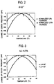
- Fig. 2 illustrates the temperature dependence of the center frequency of the surface acoustic wave device (the surface acoustic wave filter) fabricated by the above process.
- the peak temperature of the quadratic curve shifts.
- Fig. 4 shows propagation direction ⁇ vs. peak temperature relationships at the normalized thickness of 0.3%, 0.5%, and 0.75%, respectively. From Fig. 4, it is understood that in the process of transition of the propagation direction from 25 degrees to 26 degrees (or at 25.5 degrees), there is a peak temperature decrease with increasing ⁇ in an area having a small ⁇ , and there is a peak temperature increases with increasing ⁇ in an area having a large ⁇ .
- the peak temperature for the frequency temperature characteristics can thus be set in the vicinity of room temperature, thereby achieving a device excellent in temperature stability.
- the wavelength ⁇ of a surface acoustic wave at the center or resonance frequency is determined by the frequency to which the surface acoustic wave device is applied and the speed of sound of the substrate. In the preferred frequency band to which the invention is applied, however, the wavelength ⁇ is generally of the order of 8 to 60 ⁇ m. It is also to be noted that the thickness, h, of the interdigital electrode is generally of the order of 0.1 to 2 ⁇ m, because too thin an electrode results in increased electrical resistance while too thick an electrode is difficult to form, and is likely to exfoliate. Accordingly, the normalized thickness h/ ⁇ of the interdigital electrode is generally of the order of 0.17 to 25%.
- the langasite single crystal used in the invention is generally represented by the chemical formula La 3 Ga 5 SiO 14 .
- a langasite single crystal for instance, is known from Proc. IEEE International Frequency Control Sympo. vol. 1994, pp. 48-57(1994).
- the langasite single crystal is applied to a surface acoustic wave device substrate. If, in this case, the crystal cut direction is selected as mentioned above and the direction of propagation of surface acoustic waves is selected depending on the normalized thickness of the interdigital electrode, then a surface acoustic wave device having such high characteristics as mentioned above can be achieved.
- the invention is distinguishable from the conventional use of langasite single crystals.
- the langasite single crystals used herein are not always limited to that represented by the aforesaid chemical formula. For instance, at least one part of each site for La, Ga, and Si may have been substituted by other element, or the number of oxygen atoms may depart from the aforesaid stoichiometric composition.
- the langasite single crystals may contain inevitable impurities such as Al, Zr, Fe, Ce, Nd, Pt, and Ca. No particular limitation is imposed on how to produce the langasite single crystals; that is, they may be produced by ordinary single crystal growth processes, for instance, the CZ process.
- Substrate size is not particularly critical, and may generally be of the order of 4 to 10 mm in the direction of propagation of surface acoustic waves and of the order of 2 to 4 mm in the direction perpendicular thereto, and substrate thickness may be of the order of 0.2 to 0.4 mm. It is to be noted that the cut direction of the substrate is ascertainable by x-ray diffraction.
- Each of the interdigital electrodes 3 formed on the substrate 2 is a periodically striped electrode.
- the interdigital electrode is such patterned as to achieve the aforesaid preselected direction of propagation of surface acoustic waves depending on its thickness.
- the interdigital electrode may be formed as by vacuum evaporation or sputtering, using Al or Al alloys.
- the finger width of the interdigital electrode may be determined depending on the frequency to which the surface acoustic wave device is applied and the speed of sound of the substrate, and may generally be of the order of 2 to 15 ⁇ m at the frequency band to which the invention is preferably applied.
- the surface acoustic wave device of the invention lends itself well to filters used at a frequency band of 10 to 500 MHz in general, and 10 to 300 MHz in particular.
- the surface acoustic wave device of the invention is useful for making a surface acoustic wave delay element small as well, because of its low SAW velocity.
- the cut angle of the langasite single crystal substrate is optimized, it is possible to achieve a surface acoustic wave device comprising a substrate having a large electromechanical coupling factor k 2 and a slow SAW velocity.
- a surface acoustic wave device comprising a substrate having a large electromechanical coupling factor k 2 and a slow SAW velocity.
Landscapes
- Physics & Mathematics (AREA)
- Acoustics & Sound (AREA)
- Surface Acoustic Wave Elements And Circuit Networks Thereof (AREA)
Applications Claiming Priority (3)
| Application Number | Priority Date | Filing Date | Title |
|---|---|---|---|
| JP23711897 | 1997-09-02 | ||
| JP23711897 | 1997-09-02 | ||
| PCT/JP1998/002767 WO1999012257A1 (fr) | 1997-09-02 | 1998-06-22 | Appareil a ondes acoustiques de surface |
Publications (3)
| Publication Number | Publication Date |
|---|---|
| EP0955726A1 true EP0955726A1 (fr) | 1999-11-10 |
| EP0955726A4 EP0955726A4 (fr) | 2004-12-15 |
| EP0955726B1 EP0955726B1 (fr) | 2005-10-26 |
Family
ID=17010686
Family Applications (1)
| Application Number | Title | Priority Date | Filing Date |
|---|---|---|---|
| EP98928609A Expired - Lifetime EP0955726B1 (fr) | 1997-09-02 | 1998-06-22 | Appareil a ondes acoustiques de surface |
Country Status (6)
| Country | Link |
|---|---|
| US (1) | US6137207A (fr) |
| EP (1) | EP0955726B1 (fr) |
| JP (1) | JP3188480B2 (fr) |
| CN (1) | CN1138342C (fr) |
| DE (1) | DE69832041T2 (fr) |
| WO (1) | WO1999012257A1 (fr) |
Families Citing this family (8)
| Publication number | Priority date | Publication date | Assignee | Title |
|---|---|---|---|---|
| RU2099857C1 (ru) * | 1996-01-10 | 1997-12-20 | Наталья Федоровна Науменко | Высокочастотное устройство на поверхностных акустических волнах |
| CN1153100C (zh) | 1997-03-18 | 2004-06-09 | 松下电器产业株式会社 | 光学式显示装置 |
| JP2000068778A (ja) * | 1998-08-21 | 2000-03-03 | Murata Mfg Co Ltd | 表面波共振子、表面波フィルタ、共用器、通信機装置及び表面波デバイス、ならびに表面波共振子の製造方法 |
| JP3387028B2 (ja) | 1999-08-20 | 2003-03-17 | ティーディーケイ株式会社 | 弾性表面波装置 |
| WO2001035528A1 (fr) * | 1999-11-11 | 2001-05-17 | Mitsubishi Materials Corporation | Dispositif a ondes acoustiques de surface |
| US20070158660A1 (en) * | 2005-12-22 | 2007-07-12 | Acol Technologies S.A. | Optically active compositions and combinations of same with InGaN semiconductors |
| AU2013201383B2 (en) * | 2013-03-01 | 2015-07-02 | Royal Melbourne Institute Of Technology | Atomisation apparatus using surface acoustic wave generaton |
| CN111879853A (zh) * | 2020-07-16 | 2020-11-03 | 中国科学院声学研究所 | 一种剪切波模式的声表面波谐振式检测器 |
Family Cites Families (8)
| Publication number | Priority date | Publication date | Assignee | Title |
|---|---|---|---|---|
| JPS594310A (ja) * | 1982-06-30 | 1984-01-11 | Toshiba Corp | 弾性表面波装置 |
| DE3575248D1 (de) * | 1984-06-05 | 1990-02-08 | Toshiba Kawasaki Kk | Akustische oberflaechen-wellen-anordnung. |
| AT389170B (de) * | 1987-11-19 | 1989-10-25 | Avl Verbrennungskraft Messtech | Piezoelektrisches messelement |
| JP3090218B2 (ja) * | 1991-01-30 | 2000-09-18 | キンセキ株式会社 | 弾性表面波装置 |
| US5917265A (en) * | 1996-01-10 | 1999-06-29 | Sawtek Inc. | Optimal cut for saw devices on langasite |
| RU2099857C1 (ru) | 1996-01-10 | 1997-12-20 | Наталья Федоровна Науменко | Высокочастотное устройство на поверхностных акустических волнах |
| EP0810725A3 (fr) * | 1996-05-29 | 1999-10-27 | Santech Company, Limited | Plaquette et filtre à ondes acoustiques de surface |
| JPH10190407A (ja) * | 1996-10-23 | 1998-07-21 | Mitsubishi Materials Corp | 表面弾性波素子 |
-
1998
- 1998-06-22 WO PCT/JP1998/002767 patent/WO1999012257A1/fr not_active Ceased
- 1998-06-22 EP EP98928609A patent/EP0955726B1/fr not_active Expired - Lifetime
- 1998-06-22 DE DE69832041T patent/DE69832041T2/de not_active Expired - Fee Related
- 1998-06-22 CN CNB988012650A patent/CN1138342C/zh not_active Expired - Fee Related
- 1998-06-22 JP JP50210599A patent/JP3188480B2/ja not_active Expired - Fee Related
-
1999
- 1999-05-03 US US09/303,537 patent/US6137207A/en not_active Expired - Lifetime
Non-Patent Citations (2)
| Title |
|---|
| No further relevant documents disclosed * |
| See also references of WO9912257A1 * |
Also Published As
| Publication number | Publication date |
|---|---|
| WO1999012257A1 (fr) | 1999-03-11 |
| EP0955726A4 (fr) | 2004-12-15 |
| CN1237288A (zh) | 1999-12-01 |
| JP3188480B2 (ja) | 2001-07-16 |
| US6137207A (en) | 2000-10-24 |
| DE69832041D1 (de) | 2005-12-01 |
| CN1138342C (zh) | 2004-02-11 |
| DE69832041T2 (de) | 2006-07-13 |
| EP0955726B1 (fr) | 2005-10-26 |
Similar Documents
| Publication | Publication Date | Title |
|---|---|---|
| US6005325A (en) | Surface acoustic wave device | |
| US6833774B2 (en) | Surface acoustic wave filter | |
| CN110999080B (zh) | 弹性波装置、多工器、高频前端电路以及通信装置 | |
| US20080067891A1 (en) | Acoustic wave device and filter | |
| JPWO1997049182A1 (ja) | 弾性表面波装置 | |
| CN110383683B (zh) | 多工器、高频前端电路以及通信装置 | |
| KR20190108607A (ko) | 탄성파 장치, 멀티플렉서, 고주파 프론트 엔드 회로 및 통신 장치 | |
| US6940208B2 (en) | Surface acoustic wave device | |
| US6121713A (en) | Surface acoustic wave device | |
| CN112655150B (zh) | 弹性波装置、高频前端电路以及通信装置 | |
| EP0955726A1 (fr) | Appareil a ondes acoustiques de surface | |
| US5905325A (en) | Optimal cut for saw devices on langanite | |
| US6097131A (en) | Optimal cut for SAW devices on langatate | |
| US6323577B1 (en) | Saw device | |
| US6452306B1 (en) | Surface acoustic wave device and piezoelectric substrate used therefor | |
| JPWO1999012257A1 (ja) | 弾性表面波装置 | |
| US6700300B2 (en) | Surface acoustic wave device and piezoelectric substrate used therefor | |
| US6429570B1 (en) | Surface acoustic wave device | |
| US6400061B1 (en) | Surface acoustic wave device and substrate thereof | |
| CN112673570B (zh) | 弹性波装置、弹性波滤波器以及复合滤波器装置 | |
| CN223993665U (zh) | 声表面波谐振装置及滤波装置 | |
| JP3414687B2 (ja) | 弾性表面波装置用圧電基板および弾性表面波装置 | |
| JP4197620B2 (ja) | 弾性表面波装置 | |
| JP2004088631A (ja) | 圧電基板および弾性表面波装置 | |
| JPH08204500A (ja) | 弾性表面波装置 |
Legal Events
| Date | Code | Title | Description |
|---|---|---|---|
| PUAI | Public reference made under article 153(3) epc to a published international application that has entered the european phase |
Free format text: ORIGINAL CODE: 0009012 |
|
| 17P | Request for examination filed |
Effective date: 19990505 |
|
| AK | Designated contracting states |
Kind code of ref document: A1 Designated state(s): DE FR GB |
|
| A4 | Supplementary search report drawn up and despatched |
Effective date: 20041102 |
|
| RIC1 | Information provided on ipc code assigned before grant |
Ipc: 7H 03H 9/02 B Ipc: 7H 03H 9/64 B Ipc: 7H 03H 9/25 B Ipc: 7H 03H 9/145 A |
|
| GRAP | Despatch of communication of intention to grant a patent |
Free format text: ORIGINAL CODE: EPIDOSNIGR1 |
|
| GRAS | Grant fee paid |
Free format text: ORIGINAL CODE: EPIDOSNIGR3 |
|
| GRAA | (expected) grant |
Free format text: ORIGINAL CODE: 0009210 |
|
| AK | Designated contracting states |
Kind code of ref document: B1 Designated state(s): DE FR GB |
|
| REG | Reference to a national code |
Ref country code: GB Ref legal event code: FG4D |
|
| REF | Corresponds to: |
Ref document number: 69832041 Country of ref document: DE Date of ref document: 20051201 Kind code of ref document: P |
|
| ET | Fr: translation filed | ||
| PLBE | No opposition filed within time limit |
Free format text: ORIGINAL CODE: 0009261 |
|
| STAA | Information on the status of an ep patent application or granted ep patent |
Free format text: STATUS: NO OPPOSITION FILED WITHIN TIME LIMIT |
|
| 26N | No opposition filed |
Effective date: 20060727 |
|
| PGFP | Annual fee paid to national office [announced via postgrant information from national office to epo] |
Ref country code: DE Payment date: 20080626 Year of fee payment: 11 |
|
| PGFP | Annual fee paid to national office [announced via postgrant information from national office to epo] |
Ref country code: FR Payment date: 20080617 Year of fee payment: 11 |
|
| PGFP | Annual fee paid to national office [announced via postgrant information from national office to epo] |
Ref country code: GB Payment date: 20080625 Year of fee payment: 11 |
|
| GBPC | Gb: european patent ceased through non-payment of renewal fee |
Effective date: 20090622 |
|
| REG | Reference to a national code |
Ref country code: FR Ref legal event code: ST Effective date: 20100226 |
|
| PG25 | Lapsed in a contracting state [announced via postgrant information from national office to epo] |
Ref country code: FR Free format text: LAPSE BECAUSE OF NON-PAYMENT OF DUE FEES Effective date: 20090630 |
|
| PG25 | Lapsed in a contracting state [announced via postgrant information from national office to epo] |
Ref country code: GB Free format text: LAPSE BECAUSE OF NON-PAYMENT OF DUE FEES Effective date: 20090622 |
|
| PG25 | Lapsed in a contracting state [announced via postgrant information from national office to epo] |
Ref country code: DE Free format text: LAPSE BECAUSE OF NON-PAYMENT OF DUE FEES Effective date: 20100101 |