EP0957475B1 - Procede d'enregistrement optique et dispositif d'enregistrement optique - Google Patents
Procede d'enregistrement optique et dispositif d'enregistrement optique Download PDFInfo
- Publication number
- EP0957475B1 EP0957475B1 EP97949123A EP97949123A EP0957475B1 EP 0957475 B1 EP0957475 B1 EP 0957475B1 EP 97949123 A EP97949123 A EP 97949123A EP 97949123 A EP97949123 A EP 97949123A EP 0957475 B1 EP0957475 B1 EP 0957475B1
- Authority
- EP
- European Patent Office
- Prior art keywords
- mark
- recording
- optical
- pulse
- power
- Prior art date
- Legal status (The legal status is an assumption and is not a legal conclusion. Google has not performed a legal analysis and makes no representation as to the accuracy of the status listed.)
- Expired - Lifetime
Links
- 230000003287 optical effect Effects 0.000 title claims description 108
- 238000000034 method Methods 0.000 title claims description 24
- 239000010409 thin film Substances 0.000 claims description 24
- 230000003111 delayed effect Effects 0.000 claims description 18
- 230000001678 irradiating effect Effects 0.000 claims description 8
- 239000000758 substrate Substances 0.000 claims description 8
- 238000001514 detection method Methods 0.000 description 10
- 238000010586 diagram Methods 0.000 description 8
- 230000006866 deterioration Effects 0.000 description 3
- 150000004770 chalcogenides Chemical class 0.000 description 2
- 230000001934 delay Effects 0.000 description 2
- 238000001816 cooling Methods 0.000 description 1
- 230000003247 decreasing effect Effects 0.000 description 1
- 230000000694 effects Effects 0.000 description 1
- 238000010438 heat treatment Methods 0.000 description 1
- 239000000463 material Substances 0.000 description 1
- 238000002844 melting Methods 0.000 description 1
- 230000008018 melting Effects 0.000 description 1
- 239000002184 metal Substances 0.000 description 1
- 239000012782 phase change material Substances 0.000 description 1
- 239000000049 pigment Substances 0.000 description 1
- 238000002310 reflectometry Methods 0.000 description 1
- 230000002441 reversible effect Effects 0.000 description 1
- 238000002834 transmittance Methods 0.000 description 1
- 230000003313 weakening effect Effects 0.000 description 1
Images





Classifications
-
- G—PHYSICS
- G11—INFORMATION STORAGE
- G11B—INFORMATION STORAGE BASED ON RELATIVE MOVEMENT BETWEEN RECORD CARRIER AND TRANSDUCER
- G11B7/00—Recording or reproducing by optical means, e.g. recording using a thermal beam of optical radiation by modifying optical properties or the physical structure, reproducing using an optical beam at lower power by sensing optical properties; Record carriers therefor
-
- G—PHYSICS
- G11—INFORMATION STORAGE
- G11B—INFORMATION STORAGE BASED ON RELATIVE MOVEMENT BETWEEN RECORD CARRIER AND TRANSDUCER
- G11B7/00—Recording or reproducing by optical means, e.g. recording using a thermal beam of optical radiation by modifying optical properties or the physical structure, reproducing using an optical beam at lower power by sensing optical properties; Record carriers therefor
- G11B7/12—Heads, e.g. forming of the optical beam spot or modulation of the optical beam
- G11B7/125—Optical beam sources therefor, e.g. laser control circuitry specially adapted for optical storage devices; Modulators, e.g. means for controlling the size or intensity of optical spots or optical traces
- G11B7/126—Circuits, methods or arrangements for laser control or stabilisation
-
- G—PHYSICS
- G11—INFORMATION STORAGE
- G11B—INFORMATION STORAGE BASED ON RELATIVE MOVEMENT BETWEEN RECORD CARRIER AND TRANSDUCER
- G11B20/00—Signal processing not specific to the method of recording or reproducing; Circuits therefor
- G11B20/10—Digital recording or reproducing
- G11B20/10009—Improvement or modification of read or write signals
- G11B20/10046—Improvement or modification of read or write signals filtering or equalising, e.g. setting the tap weights of an FIR filter
- G11B20/10194—Improvement or modification of read or write signals filtering or equalising, e.g. setting the tap weights of an FIR filter using predistortion during writing
-
- G—PHYSICS
- G11—INFORMATION STORAGE
- G11B—INFORMATION STORAGE BASED ON RELATIVE MOVEMENT BETWEEN RECORD CARRIER AND TRANSDUCER
- G11B7/00—Recording or reproducing by optical means, e.g. recording using a thermal beam of optical radiation by modifying optical properties or the physical structure, reproducing using an optical beam at lower power by sensing optical properties; Record carriers therefor
- G11B7/004—Recording, reproducing or erasing methods; Read, write or erase circuits therefor
- G11B7/0045—Recording
-
- G—PHYSICS
- G11—INFORMATION STORAGE
- G11B—INFORMATION STORAGE BASED ON RELATIVE MOVEMENT BETWEEN RECORD CARRIER AND TRANSDUCER
- G11B7/00—Recording or reproducing by optical means, e.g. recording using a thermal beam of optical radiation by modifying optical properties or the physical structure, reproducing using an optical beam at lower power by sensing optical properties; Record carriers therefor
- G11B7/004—Recording, reproducing or erasing methods; Read, write or erase circuits therefor
- G11B7/0055—Erasing
Definitions
- This invention relates to an optical recording method and an optical recording device in which information is recorded as lengths of marks and spaces at high density by irradiating optical beams onto a recording thin film formed on a substrate.
- optical recording media capable of recording, reading and erasing information have been commercialized. Furthermore, high-density rewritable optical recording media capable of recording qualified animation have been actively researched and developed.
- Well-known rewritable optical recording media include phase-change optical recording media with recording layers either of chalcogenide thin films or semimetal thin films on a disc-shape substrate.
- the chalcogenide thin films comprise Te or Se, for example, Ge-Sb-Te, In-Se, or the like, as a base.
- the semimetal thin films comprise In-Sb or the like.
- Magneto-optical recording media having metal thin films such as Fe-Tb-Co as their recording layers also are well known. Further, there are also write-once-type optical recording media using pigment materials.
- phase-change optical recording media recording thin films comprising the above-mentioned phase-change materials are instantly irradiated with laser beams focused on submicron-order size optical spots to heat the irradiated parts partially.
- the temperature of the irradiated portion becomes equal to or higher than the crystalline temperature, the irradiated portion is changed to the crystalline state.
- the irradiated portion is melted at a temperature higher than its melting point and is quenched, its state is changed to the amorphous state.
- the crystalline state or the amorphous state is determined so as to correspond to the recording state, and the other to the erasing state (unrecorded state)
- information can be recorded reversibly by forming a pattern changing between the amorphous state and the crystalline state corresponding to information signals. Since the crystalline state and the amorphous state are different from each other in their optical characteristics, recorded signals can be read by optically detecting such different characteristics as a reflectivity change or a transmittance change.
- a magneto-optical recording medium In a magneto-optical recording medium, focused laser beams are irradiated on a magneto-optical recording thin film, so that the irradiated portions are partially heated. A magnetic field is applied to the heated portion in order to reverse the magnetizing direction of the magneto-optical recording thin film at the irradiated portions corresponding to the information to be recorded, thus recording information.
- Methods of recording data on optical recording media at a high density include a mark-length recording.
- marks with various lengths are recorded at various intervals (spaces), and the recording information is allocated to both the mark lengths and the space lengths.
- information can be recorded by setting amorphous regions as marks and crystalline regions as spaces.
- FIG. 9(a) shows a pulse shape of data to be recorded. Levels of logic 1 and logic 0 correspond to marks and spaces, respectively.
- the recording pulse shown in FIG. 9(b) is generated, thus forming the recording marks shown in FIG. 9(c) on an optical recording medium.
- the correction for delaying the front-edge of the recording pulse so as to compensate for the delay quantity 93 is made as shown in FIG. 9 (d) .
- the front-edge of the mark 91 is formed at the proper position corresponding to the front-edge of the recording data.
- the delay quantity of the front-edge of a recording pulse is determined based on the lengths of a space directly in front of the mark to be recorded and of a mark in front of the space.
- the front-edge shift can be corrected more precisely. Considering recording density, allowable error rate, processor capacity used in a device, cost, and the like, it will be decided how many spaces and marks before the mark to be recorded should be taken into account.
- the present invention provides an optical recording method as claimed in claim 1 and as claimed in claim 4.
- the optical beam power corresponding to the starting-end and the end of a recording mark is changed.
- the optical beam power is reduced so as to compensate for the increase in temperature due to heat interference.
- the power of the optical beam irradiated to the starting-end is changed according to the length of a recording mark and the length of a space directly in front of the mark (and the length of a mark in front of the space).
- the power of the optical beams mentioned above is modulated in the pulse train including the starting-end, the intermediate portion, and the end according to the lengths of marks and spaces.
- the power of the optical beam irradiated to the end is changed according to the length of a mark to be recorded and the length of a space directly behind the mark (and the length of a mark behind the space).
- the optical beam power corresponding to the starting-end or the end of a recording mark may be changed according to not only the lengths of a space and a mark directly in front of and behind the recording mark but also the lengths of at least one space and one mark further ahead and behind.
- the present invention also provides an optical recording device as claimed in claim 10 and as claimed in claim 12.
- FIG. 1 shows a block diagram of an optical recording-reading device according to Arrangement 1, not forming part of the present invention.
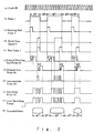
- FIG. 2 is a timing chart showing the operation of each circuit comprised in this optical recording-reading device.
- a basic pulse generator 60 is a circuit that generates basic pulses for forming recording marks.
- the basic pulse generator 60 includes a starting-end pulse generation circuit 2, a burst gate generation circuit 4, and an end pulse generation circuit 6.
- a data-length detector 61 is a circuit for detecting recording marks and the lengths of spaces and marks in front of and behind the recording marks from data 1.
- the data-length detector 61 comprises a front mark detector 40, a front space detector 41, a recording mark detector 42, a back space detector 43 and a back mark detector 44.
- a timing controller 62 is a circuit that determines the delay quantity of a starting-end pulse and an end pulse according to output signals from the data-length detector 61 and generates each pulse that has been delayed.
- the timing controller 62 comprises a stating end pulse selecting circuit 14, a starting-end pulse delaying circuit 19, an end pulse selecting circuit 21, and an end pulse delaying circuit 25.
- a pulse synthesizer 63 is a circuit that generates a final recording pulse 30 for forming marks based on output signals from the timing controller 62.
- the pulse synthesizer 63 comprises an AND gate 27 and an OR gate 36.
- a laser driver 64 is a circuit that drives a laser unit 31 corresponding to the recording pulse 30.
- the laser driver 64 comprises an erasing bias current source 32, a recording current source 33, and a switch 34.
- An optical head 65 forms recording marks by focusing the beams of the laser unit 31 on an optical recording medium 66.
- an H level and an L level are changed at a clock length unit.
- EFM having an H level period and an L level period with at least three clock periods respectively, and a code signal of (2-7).
- the H level period and the L level period in the data correspond to marks and spaces, respectively.
- Each of the detectors 40-44 in the data-length detector 61 detects mark lengths or space lengths at the clock length unit respectively. For example, when a space length is 3T or 4T in high-density recording, the heat interference between marks causes edge shift. In addition, the edge shift results in the deterioration of the error rate due to the frequency characteristics in a reading system. In fact, the influence on the error rate is determined by the combination of each mark length and space length. Therefore, the delay quantity of each pulse is determined according to each combination.
- the data 1 is input to the starting-end pulse generation circuit 2, the burst gate generation circuit 4, and the end pulse generation circuit 6 that are comprised in the basic pulse generator 60.
- the starting-end pulse generation circuit 2 generates a starting-end pulse with one clock period (see FIG. 2 (c) ) at the starting-end of the H level period in the data 1 shown in FIG. 2 (b) .
- the burst gate generation circuit 4 generates a burst gate signal 5 with a length of (a mark length - three clock periods) as shown in FIG. 2 (d) . In this case, when the mark length has three clock periods or less, the burst gate signal 5 is not generated.
- the end pulse generation circuit 6 generates an end pulse 7 with one clock period (see FIG. 2 (e) ) at the end of the H level period in the data 1.
- the data 1 is further input to a front mark detector 40, a front space detector 41, a recording mark detector 42, a back space detector 43 and a back mark detector 44 that are comprised in the data-length detector 61.
- the front space detector 41 outputs a detection signal 9 corresponding to a space length in front of a recording mark, i.e. corresponding to the L level period of three, four, or five clock periods or more in the data 1.
- the detection signal 9 is then provided to the starting-end pulse selecting circuit 14.
- the front mark detector 40 and the recording mark detector 42 provide a detection signal 8 corresponding to the front-mark length and a detection signal 10 corresponding to the recording mark length to the starting-end pulse selecting circuit 14, respectively.
- the starting-end pulse selecting circuit 14 determines the delaying time of the starting-end pulse based on each of the detection signals 8, 9, and 10, for example, according to Table 1.
- Table 1 Front Mark Length Front Space Length Recording Mark Length Delaying Time d1 3T 3T 3T a ns 4T 3T 3T b ns 5-11T 3T 3T c ns 3T 3T 4-11T d ns 4T 3T 4-11T e ns 5-11T 3T 4-11T f ns 3T 4T 3T g ns 4T 4T 3T h ns 5-11T 4T 3T i ns 3T 4T 4-11T j ns 4T 4T 4-11T k ns 5-11T 4T 4-11T l ns 3-11T 5-11T 3-11T m ns
- the delaying times a-f (ns) of a starting-end pulse are determined according to the combination of a front mark length and a recording mark length.
- the delaying times a-f (ns) of the starting-end pulse are determined according to the combination of the front mark length and the recording mark length.
- the front space length is at least 5 T, the delaying time m (ns) is determined regardless of the recording mark length and the front mark length.
- the starting-end pulse delaying circuit 19 delays a starting-end pulse 3 according to a delay signal 16 that is determined as mentioned above and is output from the starting-end pulse selecting circuit 14 and outputs the delayed starting-end pulse 20 shown in FIG. 2(f) . Consequently, the delay quantity of the starting-end pulse can be changed flexibly according to the recording mark length, the front mark length, and the front space length.
- the delay quantity of the end pulse also is determined in the same way.
- the back space detector 43 outputs a detection signal 11 corresponding to a space length behind a recording mark, i.e. corresponding to the L level period of three, four, or five clock periods or more in the data 1.
- the detection signal 11 is then provided to the end pulse selecting circuit 21.
- the back space detector 43 provides a detection signal 12 corresponding to a back mark length and the recording mark detector 42 provides a detection signal 10 corresponding to the recording mark length to the end pulse selecting circuit 21 respectively.
- the end pulse selecting circuit 21 determines the delaying time of the end pulse based on each of the detection signals 10, 11, and 12, for example, according to Table 2.
- Table 2 Back Mark Length Back Space Length Recording Mark Length Delaying Time d2 3T 3T 3T n ns 4T 3T 3T o ns 5-11T 3T 3T p ns 3T 3T 4-11T q ns 4T 3T 4-11T r ns 5-11T 3T 4-11T s ns 3T 4T 3T t ns 4T 4T 3T u ns 5-11T 4T 3T v ns 3T 4T 4-11T w ns 4T 4T 4-11T x ns 5-11T 4T 4-11T 4-11T y ns 3-11T 5-11T 3-11 T z ns
- the delaying times n-s (ns) of an end pulse are determined according to the combination of a back mark length and a recording mark length.
- the delaying times t-y (ns) of the end pulse are determined according to the combination of the back mark length and the recording mark length.
- the delaying time z (ns) is determined regardless of the recording mark length and the front mark length.
- An end pulse delaying circuit 25 delays an end pulse 7 according to a delay signal 22 that is determined as mentioned above and is output from the end pulse selecting circuit 21 and outputs the delayed end pulse 26 shown in FIG. 2(g) . Consequently, the delay quantity of the end pulse can be changed flexibly according to the recording mark length, the back mark length, and the back space length.
- the AND gate 27 in the pulse synthesizer 63 determines the AND of the burst gate signal 5 in FIG. 2(d) and the clock 28 in FIG. 2(a) and then outputs an intermediate pulse 29. In the case where the mark length is 3T or less, since the burst gate signal 5 is in the L level, the intermediate pulse 29 also is in the L level.
- the OR gate 36 determines the OR of the delayed starting-end pulse 20, the delayed end pulse 26, and the intermediate pulse 29 and then outputs the recording pulse 30 in FIG. 2(i) .
- the laser unit 31 generates an erasing power by the bias current source 32.
- the bias current source 32 is connected in parallel to a series circuit of the recording current source 33 and the switch 34.
- the switch 34 Through the on-off control by the switch 34, the laser unit 31 can be switched between the recording power and the erasing power as shown in FIG. 2(j) . Consequently, by controlling the switch 34 with the recording pulse 30, the emission power of the laser unit 31 is controlled. As a result, marks and spaces can be formed on the optical recording medium 66 as shown in FIG. 2(k) .
- the positions of the starting edge and the end-edge of a recording mark are changed according to the lengths of the recording mark and of spaces and marks in front of and behind the recording mark, thus correcting the edge shift due to heat interference. Consequently, signals with small bit errors when being read can be recorded.
- the delay quantity of a recording pulse starting-edge is determined based on a recording pulse length, a front space length, and a front mark length.
- the delay quantity of the recording pulse end is determined based on a recording pulse length, a back space length, and a back mark length.
- the preferred arrangement does not always require delaying both the starting-end and the end. Either end may be delayed as mentioned above, and the other may not be delayed or may be delayed by another method.
- the delay quantity is constant.
- the delay of the starting-end pulse and the end pulse may be controlled at each space and each mark according to the extent of the edge shift.
- marks are recorded by a plurality of pulse trains.
- the preferred arrangement is not limited to this.
- the delay of the front-edge and the end-edge can be controlled by applying the preferred arrangement also in the case where marks are recorded by one rectangular pulse.
- the delay of the starting-end pulse and the end pulse of a recording mark may be controlled.
- FIG. 3 shows a block diagram of an optical recording-reading device according to Arrangement 2, not forming part of the present invention.
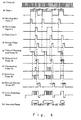
- FIG. 4 is a timing chart showing the operation of each circuit comprised in this device.
- the device of the preferred arrangement comprises a data-length detector 61, a timing controller 62, and a pulse synthesizer 63 as in Arrangement 1 shown in FIG. 1 .
- a basic pulse generator 300 comprises a bottom pulse generation circuit 301 in addition to the basic pulse generator 60 in FIG. 1 .
- a laser driver 304 comprises a bottom pulse current source 302 and a bottom switch 303 in addition to the laser driver 64 in FIG. 1 .
- a bottom pulse delaying circuit 305 is provided for controlling the output timing of the bottom pulses.
- each circuit with the same name as in the basic pulse generator 60 in FIG. 1 has the same function.
- the newly added bottom pulse generation circuit 301 generates a bottom pulse 306 shown in FIG. 4(f) from the end position of the H level period in data 1.
- the data detector 61, the timing controller 62, and the pulse synthesizer 63 have the same function as in Arrangement 1 of FIG. 1 respectively.
- the bottom pulse delaying circuit 305 generates the delayed bottom pulse 307 ( FIG. 4(k) ) obtained by delaying the bottom pulse 306 directly behind the delayed end pulse ( FIG. 4(h) ).
- a laser unit 31 generates an erasing power by a bias current source 32.
- the bias current source 32 is connected in parallel to a series circuit of a recording current source 33 and a switch 34 and further to a series circuit of the bottom pulse current source 302 and the switch 303.
- the switch 34 and the switch 303 control the current of the recording current source 33 and the current of the bottom pulse current source 302 so as to be on either on or off status respectively. Therefore, by controlling the switches 34 and 303 by the recording pulse 30 and the delayed bottom pulse 307 respectively, the laser beam 31 can be switched between the recording power, the erasing power, or the bottom power (see FIG. 4(l) ).
- a bottom pulse is added to Arrangement 1.
- the delay quantity of the end pulse is reduced and therefore the end portion of the intermediate pulse and the end pulse overlap in some cases.
- the power density of laser beams irradiated to the mark-end increases. Therefore, the temperature increases greatly, thus weakening the effect of reducing the heat interference between marks.
- the power level of the laser beams irradiated to a portion behind the recording mark is made lower than the erasing power by the bottom pulse. Therefore, the heat interference caused by conducting heat of the mark-end astern can be suppressed.
- the allowable power level of the laser beam corresponding to the bottom pulse is the level lower than the erasing power level.
- the positions of the starting-edge and the end-edge of a recording mark are changed according to the recording mark length, the space lengths and the mark lengths in front of and behind the recording mark. Therefore, the edge shift due to the heat interference is corrected, and the irradiation power of the laser beams irradiated to a portion behind the recording mark is made lower than the erasing power level for a predetermined period, thus suppressing the heat interference. Consequently, signals can be recorded with small bit errors when being read.
- FIG. 5 shows a block diagram of an optical recording-reading device according to Embodiment 1 of the present invention.
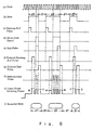
- FIG. 6 is a timing chart showing the operation of each circuit comprised in this device.
- the device of the present embodiment comprises a basic pulse generator 60 and a data-length detector 61 as in Arrangement 1 shown in FIG. 1 .
- a power setting part 70 in FIG. 5 is a circuit for setting the power of a starting-end pulse and an end pulse corresponding to a recording mark.
- the power setting part 70 comprises a starting-end pulse selecting circuit 14, a starting-end power setting circuit 52, an end pulse selecting circuit 21, and an end power setting circuit 55.
- a pulse delaying part 72 in FIG. 5 is a circuit for controlling the timing of a starting-end pulse and an end pulse.
- the pulse delaying part 72 comprises a starting-end delaying circuit 73 and an end delaying circuit 74.
- a laser driver 71 is a circuit for driving the laser unit 31 by the timing of the pulse output from the basic pulse generator 60 and by the laser power that is set in the power setting part 70.
- a bias current source 32 is connected in parallel to series circuits of an end pulse current source 40 and a switch 58, of an intermediate pulse current source 41 and a switch 57, and of a starting-end pulse current source 42 and a switch 58.
- an H level and an L level are changed at a clock length unit in Data 1.
- EFM having an H level period and an L level period that are at least three clock periods, and a code signal of (2-7).
- the H level period and the L level period in the data correspond to marks and spaces, respectively.
- Each of the detectors 40-44 in the data-length detector 61 detects mark lengths or space lengths at the clock length unit respectively. For example, when a space length is 3T or 4T in high-density recording, the heat interference between marks causes edge shift. In addition, the edge shift results in the deterioration of the error rate due to the frequency characteristics in a reading system. In fact, the influence on the error rate is determined by the combination of each mark length and space length. Therefore, the laser power corresponding to each pulse is determined according to each combination.
- the basic pulse generator 60 has the same operation as in Arrangement 1.
- the starting-end pulse selecting circuit 14 determines the laser power (for instance, a peak value) corresponding to a starting-end pulse based on each of the output signals 8, 9, and 10 from a front mark detector 40, a front space detector 41, and a recording mark detector 42 respectively, for example, according to Table 3.
- the laser powers (peak values) a-f corresponding to a starting-end pulse are determined according to the combination of a front mark length and a recording mark length.
- the laser powers g-l corresponding to a starting-end pulse are determined according to the combination of the front mark length and the recording mark length.
- the laser power m corresponding to a starting-end pulse is determined regardless of the recording mark length and the front mark length.
- the starting-end power setting circuit 52 controls the starting-end pulse current source 42 so that the laser unit 31 emits beams at the laser power determined as mentioned above.
- the end pulse selecting circuit 21 determines the laser power (for instance, a peak value) corresponding to an end pulse based on each of the output signals 10, 11, and 12 of the recording mark detector 42, a back space detector 43, and a back mark detector 44 respectively, for example, according to Table 4.
- the laser powers (peak value) n-s corresponding to an end pulse are determined according to the combination of a recording mark length and a back mark length.
- the laser powers t-y corresponding to an end pulse are determined according to the combination of the recording mark length and the back mark length.
- the laser power n corresponding to an end pulse is determined regardless of the recording mark length and the back mark length.
- the end power setting circuit 55 controls the end pulse current source 40 so that the laser unit 31 emits beams at the laser power determined as mentioned above.
- the peak value of the intermediate pulse 29 is fixed to a suitable value.
- a starting-end delaying circuit 73 in FIG. 5 controls the timing for generating starting-end pulses. In FIG. 6 , the delay quantity is set to 1.5T.
- An end delaying circuit 74 controls the timing for generating end pulses. In FIG. 6 , the delay quantity is set to 1T.
- a laser driver 71 in FIG. 5 comprises series circuits of a starting-end pulse current source 42 and a switch 56, of an intermediate pulse current source 41 and a switch 57, and of an end pulse current source 40 and a switch 58, and a bias current source 32 connected in parallel to the series circuits.
- the starting-end pulse, the intermediate pulse, and the end pulse control the three switches 56, 57, and 58, respectively. Consequently, the laser unit 31 can emit laser beams for one recording mark at the starting-end power, the intermediate power, and the end power, each of which has an independent peak value as shown in FIG. 6(i) .
- the peak values of the laser power for recording marks are controlled at the mark starting-end, at the intermediate portion, and at the end independently according to the recording mark length and the space lengths and mark lengths in front of and behind the recording mark. Therefore, the edge shift due to heat interference can be suppressed. As a result, signals can be recorded with small bit errors when being read.
- the laser powers at the starting-end and at the end are set to be constant as to data with a space of at least 5 T.
- the present invention is not limited to this.
- the laser power at the starting-end of a recording pulse is changed according to the recording pulse length, the front space length, and the front mark length.
- the laser power at the end of the recording pulse is changed according to the recording pulse length, the back space length, and the back mark length.
- the laser power only at either end may be changed as mentioned above, and the laser power at the other end may be constant or may be changed by another method.
- FIG. 7 shows a block diagram of an optical recording-reading device according to Embodiment 2 of the present invention.
- FIG. 8 is a timing chart showing the operation of each circuit comprised in this device.
- FIG. 7 comprises a data-length detector 61 and a power setting part 70 as in Embodiment 1 shown in FIG. 5 .
- the present embodiment further comprises a basic pulse generator 300 in which a bottom pulse generation circuit 301 is added, a pulse delaying part 700 in which a bottom pulse delaying circuit 305 is added, and a laser driver 701 in which a bottom pulse current source 302 and a switch 303 are added.
- each circuit with the same name as in the basic pulse generator 60 in FIG. 5 has the same function.
- the newly added bottom pulse generation circuit 301 generates a bottom pulse 306 shown in FIG. 8(f) from the end position of the H level period in data 1.
- the data detector 61 and the power setting part 70 have the same function as in Embodiment 1 shown in FIG. 5 respectively.
- the bottom pulse delaying circuit 305 controls the timing of the bottom pulse, and the delayed bottom pulse 307 ( FIG. 8(j) ) obtained by delaying the bottom pulse 306 is generated just behind the delayed end pulse ( FIG. 8(h) ).
- a laser unit 31 generates an erasing power by a bias current source 32.
- This bias current source 32 is connected in parallel to series circuits of a starting-end pulse current source 42 and a switch 56, of an intermediate pulse current source 41 and a switch 57, of an end pulse current source 40 and a switch 58, and of a bottom current source 302 and a switch 303.
- a delayed starting-end pulse, an intermediate pulse, a delayed end pulse, and a delayed bottom pulse control the on-off status of the four switches respectively. Therefore, the laser unit 31 can emit laser beams for one mark at a starting-end power, an intermediate power, an end power and a bottom power as shown in FIG. 8(k) .
- the use of an optical head 65 containing the laser unit 31 enables the marks and spaces shown in FIG. 8(l) to be formed on an optical recording medium 66.
- the bottom pulse is added to Embodiment 1.
- the power peak values at the starting-end and at the end are decreased to the lower limit of the power for forming a suitable mark by recording characteristics, linear velocity when recording information, and the like in the optical recording medium 66, the heat interference between marks can not be suppressed sufficiently in some cases.
- the laser power irradiated to a portion behind the recording mark is made lower than the erasing power by the bottom pulse. Therefore, the heat interference caused by conducting heat of the mark-end behind can be suppressed efficiently.
- An allowable power level of the laser beam corresponding to the bottom pulse is the level lower than the erasing power level.
- the peak values of the laser power for recording marks are controlled at the mark starting-end, the intermediate portion, and the end independently according to the recording mark length and the space lengths and mark lengths in front of and behind the recording mark. Therefore, the edge shift due to the heat interference is corrected, and the irradiation power of the laser beams irradiated to a portion behind the recording mark is made lower than the erasing power level for a predetermined period, thus suppressing the heat interference. Consequently, signals can be recorded with small bit errors when being read.
- the edge shift of the recording marks can be corrected or controlled, thus reducing bit errors of read signals. Consequently, the data recording density can be further increased and the capacity of an optical recording medium can be increased.
Landscapes
- Physics & Mathematics (AREA)
- Optics & Photonics (AREA)
- Engineering & Computer Science (AREA)
- Signal Processing (AREA)
- Optical Recording Or Reproduction (AREA)
- Optical Head (AREA)
Claims (14)
- Procédé d'enregistrement optique pour enregistrer des informations sur un support d'enregistrement optique ayant un film mince d'enregistrement sur un substrat, l'état du film mince d'enregistrement étant changé en irradiant des faisceaux optiques,
dans lequel afin d'enregistrer les informations sur le film mince d'enregistrement en tant que longueurs de marques et d'espaces, lors de l'irradiation des faisceaux optiques sur le film mince d'enregistrement, la puissance des faisceaux optiques étant modulée en un train d'impulsions incluant une extrémité de début, une portion intermédiaire, et une fin selon les longueurs des marques et d'espaces, la puissance d'un faisceau optique irradié vers l'extrémité de début est modifiée selon la longueur d'un espace directement devant une marque à enregistrer, caractérisé en ce que la puissance dudit faisceau optique irradié vers ladite extrémité de début est également modifiée selon la longueur de la marque à enregistrer. - Procédé d'enregistrement optique de la revendication 1,
dans lequel la puissance du faisceau optique irradié vers l'extrémité de début est également selon modifiée la longueur d'une marque devant l'espace. - Procédé d'enregistrement optique de la revendication 1 où 2,
dans lequel la puissance du faisceau optique irradié vers l'extrémité de début est également modifiée selon la longueur d'au moins un espace et une marque qui est davantage à l'avant. - Procédé d'enregistrement optique pour enregistrer des informations sur un support d'enregistrement optique ayant un film mince d'enregistrement sur un substrat, l'état du film mince d'enregistrement étant changé en irradiant des faisceaux optiques,
dans lequel afin d'enregistrer les informations sur le film mince d'enregistrement en tant que longueurs de marques et d'espaces, lors d'une irradiation de faisceaux optiques sur le film mince d'enregistrement, la puissance des faisceaux optiques étant modulée en un train d'impulsions incluant une extrémité de début, une portion intermédiaire, et une fin selon les longueurs des marques et d'espaces, caractérisé en ce que la puissance d'un faisceau optique irradié vers la fin est modifiée selon les longueurs d'une marque à enregistrer et d'un espace directement derrière la marque. - Procédé d'enregistrement optique de la revendication 4,
dans lequel la puissance du faisceau optique irradié vers la fin est également modifiée selon la longueur d'une marque derrière l'espace. - Support d'enregistrement optique de la revendication 5,
dans lequel la puissance du faisceau optique irradié vers la fin est également modifiée selon la longueur d'au moins un espace et une marque qui est davantage à l'arrière. - Procédé d'enregistrement optique de la revendication 5,
dans lequel la puissance d'irradiation des faisceaux optiques est modulée entre un niveau d'enregistrement et un niveau d'effacement inférieur au niveau d'enregistrement, et la puissance d'un faisceau optique irradié à une portion derrière la marque est rendue inférieure au niveau d'effacement pendant une période prédéterminée. - Procédé d'enregistrement optique de la revendication 4,
dans lequel la puissance d'un faisceau optique irradié vers l'extrémité de début est modifiée selon les longueurs d'une marque à enregistrer et d'un espace directement devant la marque. - Procédé d'enregistrement optique de la revendication 5,
dans lequel la puissance d'un faisceau optique irradié vers l'extrémité de début est modifiée selon les longueurs d'une marque à enregistrer, d'un espace directement devant la marque, et d'une marque devant l'espace. - Dispositif d'enregistrement optique dans lequel afin d'enregistrer des informations sur un support (66) d'enregistrement optique ayant un film mince d'enregistrement sur un substrat, l'état du film mince d'enregistrement étant changé en irradiant des faisceaux optiques sur un substrat, les informations sont enregistrées sur le film mince d'enregistrement en tant que longueurs de marques et d'espaces par des faisceaux optiques, la puissance des faisceaux optiques étant modulée en un train d'impulsions, le dispositif comprenant:un générateur (60) d'impulsions basiques qui génère une impulsion d'extrémité de début correspondant à l'extrémité de début de la marque, et une impulsion de fin correspondant à la fin de la marque, et au moins une impulsion intermédiaire correspondant à la portion intermédiaire de la marque,un détecteur (61) de marque d'enregistrement qui détecte la longueur d'une marque d'enregistrement;un détecteur (41) d'espace avant qui détecte la longueur d'un espace directement devant la marque d'enregistrement;un circuit (52) d'établissement de puissance d'extrémité de début qui établit la puissance de faisceau optique correspondant à l'impulsion d'extrémité de début sur la base du signal délivré en sortie à partir du détecteur (41) d'espace avant; etun pilote laser (71) qui module la puissance de faisceau optique sur la base des signaux délivrés en sortie à partir du générateur (60) d'impulsions basiques et du circuit (52) d'établissement de puissance d'extrémité de début;caractérisé en ce que le circuit (52) d'établissement de puissance d'extrémité de début établit également la puissance de faisceau optique correspondant à l'impulsion d'extrémité de début sur la base du signal délivré en sortie à partir du détecteur (61) de marque d'enregistrement.
- Dispositif d'enregistrement optique selon la revendication 10, comprenant en plus un détecteur (40) de marque avant qui détecte la longueur d'une marque devant l'espace directement devant la marque d'enregistrement, dans lequel le circuit (52) d'établissement de puissance d'extrémité de début établit la puissance de faisceau optique correspondant à l'impulsion d'extrémité de début sur la base de signaux délivrés en sortie à partir du détecteur (61) de marque d'enregistrement, du détecteur (41) d'espace avant, et du détecteur (40) de marque avant.
- Dispositif d'enregistrement optique dans lequel afin d'enregistrer des informations sur un support d'enregistrement optique (66) ayant un film mince d'enregistrement sur un substrat, l'état du film mince d'enregistrement étant changé en irradiant des faisceaux optiques sur un substrat, les informations sont enregistrées sur le film mince d'enregistrement en tant que longueurs de marques et d'espaces par des faisceaux optiques, la puissance des faisceaux optiques étant modulée en un train d'impulsions, le dispositif comprenant:un générateur (60) d'impulsions basiques qui génère une impulsion d'extrémité de début correspondant à l'extrémité de début de la marque, et une impulsion de fin correspondant à la fin de la marque, et au moins une impulsion intermédiaire correspondant à la portion intermédiaire de la marque,un détecteur (61) de marque d'enregistrement qui détecte la longueur d'une marque d'enregistrement;un pilote laser (71) qui module la puissance du faisceau optique sur la base du signal délivré en sortie à partir du générateur (60) d'impulsions basiques;ledit dispositif caractérisé en ce qu'il comprend:un détecteur (41) d'espace arrière qui détecte la longueur d'un espace directement derrière la marque d'enregistrement;un circuit (55) d'établissement de puissance de fin qui établit la puissance de faisceau optique correspondant à l'impulsion de fin sur la base de signaux délivrés en sortie à partir du détecteur (61) de marque d'enregistrement et du détecteur (43) d'espace arrière; etoù le pilote laser (71) module également la puissance de faisceau optique sur la base du signal délivré en sortie à partir du circuit (55) d'établissement de puissance de fin.
- Dispositif d'enregistrement optique selon la revendication 12, comprenant en plus un détecteur (44) de marque arrière qui détecte la longueur d'une marque derrière l'espace directement derrière la marque d'enregistrement,
dans lequel le circuit (55) d'établissement de puissance de fin établit la puissance de faisceau optique correspondant à l'impulsion de fin sur la base de signaux délivrés en sortie à partir du détecteur (61) de marque d'enregistrement, du détecteur (43) d'espace arrière, et du détecteur (44) de marque arrière. - Dispositif d'enregistrement optique selon la revendication 13, comprenant en plus un circuit (305) de retardement d'impulsions de fond qui génère une impulsion de fond retardée obtenue en retardant une impulsion dé fond par une largeur prédéterminée selon le retard de l'impulsion de fin,
dans lequel le générateur (60) d'impulsions basiques génère l'impulsion de fond derrière la marque d'enregistrement, et le pilote laser (71) module la puissance de faisceau optique sur la base d'un signal délivré en sortie à partir du générateur d'impulsions basiques, un signal délivré en sortie à partir du circuit (55) d'établissement de puissance de fin, et l'impulsion de fond retardée.
Applications Claiming Priority (3)
| Application Number | Priority Date | Filing Date | Title |
|---|---|---|---|
| JP34101496 | 1996-12-20 | ||
| JP34101496 | 1996-12-20 | ||
| PCT/JP1997/004663 WO1998028735A1 (fr) | 1996-12-20 | 1997-12-17 | Procede d'enregistrement optique et dispositif d'enregistrement optique |
Publications (3)
| Publication Number | Publication Date |
|---|---|
| EP0957475A1 EP0957475A1 (fr) | 1999-11-17 |
| EP0957475A4 EP0957475A4 (fr) | 2006-08-02 |
| EP0957475B1 true EP0957475B1 (fr) | 2009-03-04 |
Family
ID=18342422
Family Applications (1)
| Application Number | Title | Priority Date | Filing Date |
|---|---|---|---|
| EP97949123A Expired - Lifetime EP0957475B1 (fr) | 1996-12-20 | 1997-12-17 | Procede d'enregistrement optique et dispositif d'enregistrement optique |
Country Status (7)
| Country | Link |
|---|---|
| US (3) | US6345026B1 (fr) |
| EP (1) | EP0957475B1 (fr) |
| KR (1) | KR100358507B1 (fr) |
| CN (2) | CN1178211C (fr) |
| DE (1) | DE69739287D1 (fr) |
| ID (1) | ID21808A (fr) |
| WO (1) | WO1998028735A1 (fr) |
Families Citing this family (43)
| Publication number | Priority date | Publication date | Assignee | Title |
|---|---|---|---|---|
| JP3023310B2 (ja) | 1996-05-31 | 2000-03-21 | 松下電器産業株式会社 | 光学的情報記録媒体の記録再生方法および記録再生装置 |
| US6711105B1 (en) * | 1996-05-31 | 2004-03-23 | Matsushita Electric Industrial Co., Ltd. | Method and apparatus for writing and reading optical recording medium |
| US6243339B1 (en) * | 1997-08-12 | 2001-06-05 | U.S. Philips Corporation | Method and device for writing optical record carriers |
| US7391698B2 (en) | 1997-12-30 | 2008-06-24 | Samsung Electronics Co., Ltd. | Adaptive writing method for high-density optical recording apparatus and circuit thereof |
| US7158461B1 (en) | 1997-12-30 | 2007-01-02 | Samsung Electronics Co., Ltd. | Adaptive writing method for high-density optical recording apparatus and circuit thereof |
| KR100354732B1 (ko) * | 1998-04-03 | 2002-11-18 | 삼성전자 주식회사 | 고밀도광기록기기를위한적응적인기록방법및그장치 |
| KR100342112B1 (ko) * | 1998-11-06 | 2002-06-26 | 마츠시타 덴끼 산교 가부시키가이샤 | 광 디스크의 기록 펄스 조건을 구하는 방법 및 장치 |
| JP4075185B2 (ja) * | 1999-01-29 | 2008-04-16 | 松下電器産業株式会社 | 光学的情報記録再生方法及び光学的情報記録再生装置 |
| WO2001004885A1 (fr) * | 1999-07-07 | 2001-01-18 | Koninklijke Philips Electronics N.V. | Procede et dispositif d'ecriture de marques sur une couche d'information d'un support d'enregistrement optique |
| ID29227A (id) * | 1999-07-15 | 2001-08-16 | Koninkl Philips Electronics Nv | Metode-metode dan alat-alat untuk merekam tanda-tanda dalam satu lapisan informasi dari satu pembawa rekaman optik, dan pembawa-pembawa rekaman yang digunakan |
| US7272094B2 (en) * | 1999-07-15 | 2007-09-18 | Koninklike Philips Electronics N.V. | Methods and devices for recording marks in an information layer of an optical record carrier, and record carriers for use therein |
| DE60133571T2 (de) * | 2000-10-05 | 2009-05-14 | Panasonic Corp., Kadoma | Optisches aufzeichnungsmedium, verfahren zur aufzeichnung auf einem optischen aufzeichnungsmedium und vorrichtung zur aufzeichnung auf einem optischen aufzeichnungsmedium |
| JP4405115B2 (ja) | 2001-09-03 | 2010-01-27 | パイオニア株式会社 | 情報記録装置および情報記録方法 |
| EP1808854B8 (fr) * | 2001-10-22 | 2012-06-27 | Ricoh Company, Ltd. | Unité de commande de source lumineuse et appareil de stockage optique |
| EP1449208A2 (fr) * | 2001-11-15 | 2004-08-25 | Koninklijke Philips Electronics N.V. | Procede d'enregistrement sur support d'enregistrement optique et appareil d'enregistrement |
| JP3740413B2 (ja) * | 2001-12-20 | 2006-02-01 | 株式会社日立製作所 | 高周波重畳方法およびこれを用いた光ディスク装置 |
| JP2003208713A (ja) * | 2002-01-16 | 2003-07-25 | Tdk Corp | 光記録媒体への情報記録方法、光記録媒体及び情報記録/再生装置 |
| US7376064B2 (en) * | 2002-02-25 | 2008-05-20 | Samsung Electronics Co., Ltd. | Method and apparatus for recording data on optical recording medium |
| JP3912664B2 (ja) * | 2002-02-28 | 2007-05-09 | Tdk株式会社 | 光記録媒体への情報記録方法、情報記録装置及び光記録媒体 |
| KR100429884B1 (ko) * | 2002-03-18 | 2004-05-03 | 삼성전자주식회사 | 광 기록매체에 데이터를 기록하는 방법 및 그 장치 |
| DE60326225D1 (de) | 2002-04-19 | 2009-04-02 | Panasonic Corp | Verfahren zum aufzeichnen optischer informationen, aufzeichnungseinrichtung für optische informationen und aufzeichnungsmedium für optische informationen |
| TWI254934B (en) | 2002-04-26 | 2006-05-11 | Tdk Corp | Optical recording medium and method for optically recording data in the same |
| JP3839352B2 (ja) * | 2002-05-22 | 2006-11-01 | 株式会社日立製作所 | 情報記録媒体並びに情報再生方法及び装置 |
| JP4282285B2 (ja) * | 2002-08-12 | 2009-06-17 | Tdk株式会社 | 光記録媒体及び光記録方法 |
| JP2004103100A (ja) * | 2002-09-09 | 2004-04-02 | Tdk Corp | 光記録媒体への情報記録方法、情報記録装置及び光記録媒体 |
| JP2004171642A (ja) | 2002-11-19 | 2004-06-17 | Tdk Corp | 光記録媒体、光記録方法及び光記録装置 |
| US20050213467A1 (en) * | 2002-12-17 | 2005-09-29 | Yoshihiro Noda | Optical recording medium, and recording/reading method and recording/reading apparatus for optical recording medium |
| JP3998643B2 (ja) * | 2003-06-30 | 2007-10-31 | 東芝マイクロエレクトロニクス株式会社 | レーザ制御装置及び光ディスク装置 |
| JP2005038559A (ja) * | 2003-07-18 | 2005-02-10 | Sony Corp | 情報記録装置及び方法 |
| JP3732499B2 (ja) * | 2003-08-26 | 2006-01-05 | 株式会社リコー | 色素系追記型dvd媒体の記録再生方法及び装置 |
| WO2005041175A1 (fr) * | 2003-10-27 | 2005-05-06 | Pioneer Corporation | Dispositif d'enregistrement d'informations et procede d'enregistrement d'informations |
| US7823132B2 (en) * | 2004-09-29 | 2010-10-26 | Microsoft Corporation | Automated test case verification that is loosely coupled with respect to automated test case execution |
| US7006420B1 (en) | 2005-02-17 | 2006-02-28 | Mediatek Incorporation | Method for tuning write strategy parameters of an optical storage device, and system thereof |
| US8369199B2 (en) * | 2005-02-17 | 2013-02-05 | Mediatek Inc. | Methods and systems for tuning at least one write strategy parameter of an optical storage device |
| JP2007141391A (ja) * | 2005-11-21 | 2007-06-07 | Hitachi Ltd | 光ディスク記録方法、光ディスク記録装置及び光ディスク |
| WO2007105139A1 (fr) * | 2006-03-13 | 2007-09-20 | Koninklijke Philips Electronics N. V. | Commande de puissance en temps réel pour des pilotes d'enregistrement optique |
| JP2007317343A (ja) * | 2006-04-28 | 2007-12-06 | Sharp Corp | 記録パラメータ設定装置、そのプログラムおよび該プログラムを記録したコンピュータ読取り可能な記録媒体、情報記録媒体、ならびに記録パラメータ設定方法 |
| US8414637B2 (en) * | 2006-09-08 | 2013-04-09 | Boston Scientific Scimed, Inc. | Stent |
| JP2008097799A (ja) * | 2006-09-14 | 2008-04-24 | Ricoh Co Ltd | 情報記録方法、情報記録媒体、及び情報記録装置 |
| JP5189064B2 (ja) * | 2009-11-26 | 2013-04-24 | 日立コンシューマエレクトロニクス株式会社 | 光ディスク記録方法及び光ディスク記録装置 |
| JP2010118148A (ja) * | 2010-03-05 | 2010-05-27 | Hitachi Ltd | 光ディスク記録方法、光ディスク記録装置及び光ディスク |
| JP2011014237A (ja) * | 2010-10-22 | 2011-01-20 | Hitachi Consumer Electronics Co Ltd | 光ディスク記録方法、光ディスク記録装置及び光ディスク |
| US8837264B2 (en) * | 2011-04-14 | 2014-09-16 | Panasonic Corporation | Optical information device, optical disc driving device, optical information recording device, optical information reproducing device, gap control method, and optical pickup |
Family Cites Families (23)
| Publication number | Priority date | Publication date | Assignee | Title |
|---|---|---|---|---|
| KR910003460B1 (ko) * | 1987-02-12 | 1991-05-31 | 가부시기가이샤 히다찌세이사꾸쇼 | 광학식 정보기록 장치 |
| JPH0810489B2 (ja) | 1987-03-19 | 1996-01-31 | 松下電器産業株式会社 | 光ディスクの記録方法及び光ディスク装置 |
| JP2649923B2 (ja) * | 1987-08-31 | 1997-09-03 | 株式会社日立製作所 | 光学的情報記録装置 |
| JP2684657B2 (ja) * | 1987-11-13 | 1997-12-03 | ヤマハ株式会社 | 光ディスク記録方法 |
| JP2650357B2 (ja) | 1988-09-30 | 1997-09-03 | 松下電器産業株式会社 | 光学情報記録部材の記録方法 |
| JPH0810490B2 (ja) * | 1989-03-20 | 1996-01-31 | 富士通株式会社 | 光ディスク情報書込制御方法およびその装置 |
| US5216657A (en) | 1989-09-19 | 1993-06-01 | Matsushita Electric Industrial Co., Ltd. | Method and apparatus for timing variable optical information recording |
| US5513165A (en) * | 1990-06-29 | 1996-04-30 | Hitachi, Ltd. | Method for controlling the farm of a magnetic domain of a magneto-optical disk using pre-write testing |
| JPH04153919A (ja) | 1990-10-16 | 1992-05-27 | Nippon Telegr & Teleph Corp <Ntt> | 書換型光ディスクの記録方法 |
| JPH05101389A (ja) | 1991-10-02 | 1993-04-23 | Matsushita Electric Ind Co Ltd | 光デイスク装置及び光デイスクの記録方法 |
| JP3165216B2 (ja) * | 1992-02-21 | 2001-05-14 | 株式会社リコー | マークエッジ記録方法及びその装置 |
| US5412626A (en) * | 1992-03-23 | 1995-05-02 | Matsushita Electric Industrial Co., Ltd. | Method of recording optical information with selective correction in pulse waveform and a recording system therefor |
| JPH05274675A (ja) | 1992-03-27 | 1993-10-22 | Hitachi Electron Eng Co Ltd | 光ディスクの検査方法 |
| JP2679596B2 (ja) * | 1993-11-09 | 1997-11-19 | 松下電器産業株式会社 | ディスク記録方法およびディスク記録装置 |
| JP2684952B2 (ja) | 1993-04-07 | 1997-12-03 | 松下電器産業株式会社 | ディスク記録方法およびディスク記録装置 |
| US5490126A (en) * | 1993-04-07 | 1996-02-06 | Matsushita Electric Industrial Co., Ltd. | Apparatus for recording and reproducing data on a disk |
| DE4311683C2 (de) * | 1993-04-08 | 1996-05-02 | Sonopress Prod | Plattenförmiger optischer Speicher und Verfahren zu dessen Herstellung |
| EP0628952B1 (fr) | 1993-06-08 | 2002-02-20 | Matsushita Electric Industrial Co., Ltd. | Disque optique et appareil d'enregistrement et de reproduction d'information |
| EP0648049A1 (fr) | 1993-10-08 | 1995-04-12 | Hitachi, Ltd. | Procédé et appareil d'enregistrement et reproduction d'information |
| JP3138610B2 (ja) * | 1995-04-13 | 2001-02-26 | 株式会社リコー | 相変化型光ディスク用記録方法 |
| DE69618680T2 (de) * | 1995-10-09 | 2002-08-14 | Matsushita Electric Industrial Co., Ltd. | Aufnahmemethode und Aufnahmeeinheit für optische Information |
| US5985604A (en) * | 1997-02-24 | 1999-11-16 | Incyte Pharmaceuticals, Inc. | Human sodium-dependent phosphate cotransporter |
| JP3076033B1 (ja) * | 1998-09-14 | 2000-08-14 | 松下電器産業株式会社 | 光学情報の記録再生装置および情報記録媒体 |
-
1997
- 1997-12-17 EP EP97949123A patent/EP0957475B1/fr not_active Expired - Lifetime
- 1997-12-17 KR KR10-1998-0710186A patent/KR100358507B1/ko not_active Expired - Fee Related
- 1997-12-17 CN CNB971935033A patent/CN1178211C/zh not_active Expired - Fee Related
- 1997-12-17 ID IDW980100D patent/ID21808A/id unknown
- 1997-12-17 CN CNB2004100831590A patent/CN1295686C/zh not_active Expired - Fee Related
- 1997-12-17 DE DE69739287T patent/DE69739287D1/de not_active Expired - Lifetime
- 1997-12-17 WO PCT/JP1997/004663 patent/WO1998028735A1/fr not_active Ceased
- 1997-12-17 US US09/155,661 patent/US6345026B1/en not_active Expired - Lifetime
-
2001
- 2001-12-17 US US10/025,664 patent/US6584054B2/en not_active Expired - Lifetime
-
2003
- 2003-04-28 US US10/425,055 patent/US6762985B2/en not_active Expired - Lifetime
Also Published As
| Publication number | Publication date |
|---|---|
| US20020080703A1 (en) | 2002-06-27 |
| EP0957475A1 (fr) | 1999-11-17 |
| US6762985B2 (en) | 2004-07-13 |
| EP0957475A4 (fr) | 2006-08-02 |
| KR100358507B1 (ko) | 2003-03-03 |
| CN1178211C (zh) | 2004-12-01 |
| KR20000016590A (ko) | 2000-03-25 |
| CN1215493A (zh) | 1999-04-28 |
| CN1591597A (zh) | 2005-03-09 |
| US6584054B2 (en) | 2003-06-24 |
| WO1998028735A1 (fr) | 1998-07-02 |
| US6345026B1 (en) | 2002-02-05 |
| DE69739287D1 (de) | 2009-04-16 |
| CN1295686C (zh) | 2007-01-17 |
| US20030193867A1 (en) | 2003-10-16 |
| ID21808A (id) | 1999-07-29 |
Similar Documents
| Publication | Publication Date | Title |
|---|---|---|
| US6345026B1 (en) | Optical recording method and optical recorder | |
| US5636194A (en) | Method of recording and reproducing data on a disk | |
| EP1282117B1 (fr) | Procédé et circuit d'écriture adaptive pour un appareil d'enregistrement optique à haute densité | |
| EP0991060B1 (fr) | Support d'enregistrement d'informations optiques, appareil d'enregistrement d'informations optiques, et procédé d'enregistrement d'un signal d'essai sur ledit support | |
| US5412626A (en) | Method of recording optical information with selective correction in pulse waveform and a recording system therefor | |
| JP2679596B2 (ja) | ディスク記録方法およびディスク記録装置 | |
| KR20050062464A (ko) | 광 데이터 기록 방법 및 광 데이터 기록 장치 | |
| JP2684952B2 (ja) | ディスク記録方法およびディスク記録装置 | |
| US7116623B2 (en) | Optical information recording method, optical information recording device and optical information recording medium | |
| EP1347444B1 (fr) | Procédé et appareil d'enregistrement de données sur un support d'enregistrement optique | |
| EP0716415B1 (fr) | Méthode d'enregistrement de données sur un disque optique de type à changement de phase | |
| US20030142606A1 (en) | Information recording apparatus and method | |
| EP1811505B1 (fr) | Procédé et appareil d'enregistrement de données sur un support d'enregistrement optique | |
| CN101299336B (zh) | 数据记录方法和数据再现方法 | |
| EP1612779B1 (fr) | Procédé d'enregistrement sur des supports d'enregistrement optiques, et dispositif d'enregistrement optique | |
| KR100996038B1 (ko) | 정보 기록 매체의 기록 장치, 정보 기록 매체, 정보 기록 매체의 기록 방법, 정보 기록 매체의 기록용 프로그램을 기록한 컴퓨터 판독 가능한 기록 매체 | |
| US7193947B1 (en) | Optical information recording method, optical information recording device and optical information recording medium | |
| JPWO1998028735A1 (ja) | 光記録方法及び光記録装置 | |
| JP2005032295A (ja) | 情報の記録方法 |
Legal Events
| Date | Code | Title | Description |
|---|---|---|---|
| PUAI | Public reference made under article 153(3) epc to a published international application that has entered the european phase |
Free format text: ORIGINAL CODE: 0009012 |
|
| 17P | Request for examination filed |
Effective date: 19990305 |
|
| AK | Designated contracting states |
Kind code of ref document: A1 Designated state(s): DE FR GB |
|
| A4 | Supplementary search report drawn up and despatched |
Effective date: 20060629 |
|
| 17Q | First examination report despatched |
Effective date: 20061027 |
|
| 17Q | First examination report despatched |
Effective date: 20061027 |
|
| GRAP | Despatch of communication of intention to grant a patent |
Free format text: ORIGINAL CODE: EPIDOSNIGR1 |
|
| RAP1 | Party data changed (applicant data changed or rights of an application transferred) |
Owner name: PANASONIC CORPORATION |
|
| GRAS | Grant fee paid |
Free format text: ORIGINAL CODE: EPIDOSNIGR3 |
|
| GRAA | (expected) grant |
Free format text: ORIGINAL CODE: 0009210 |
|
| AK | Designated contracting states |
Kind code of ref document: B1 Designated state(s): DE FR GB |
|
| REG | Reference to a national code |
Ref country code: GB Ref legal event code: FG4D |
|
| REF | Corresponds to: |
Ref document number: 69739287 Country of ref document: DE Date of ref document: 20090416 Kind code of ref document: P |
|
| PLBE | No opposition filed within time limit |
Free format text: ORIGINAL CODE: 0009261 |
|
| STAA | Information on the status of an ep patent application or granted ep patent |
Free format text: STATUS: NO OPPOSITION FILED WITHIN TIME LIMIT |
|
| 26N | No opposition filed |
Effective date: 20091207 |
|
| PGFP | Annual fee paid to national office [announced via postgrant information from national office to epo] |
Ref country code: GB Payment date: 20101215 Year of fee payment: 14 |
|
| PGFP | Annual fee paid to national office [announced via postgrant information from national office to epo] |
Ref country code: DE Payment date: 20101215 Year of fee payment: 14 |
|
| PGFP | Annual fee paid to national office [announced via postgrant information from national office to epo] |
Ref country code: FR Payment date: 20111219 Year of fee payment: 15 |
|
| GBPC | Gb: european patent ceased through non-payment of renewal fee |
Effective date: 20121217 |
|
| REG | Reference to a national code |
Ref country code: FR Ref legal event code: ST Effective date: 20130830 |
|
| REG | Reference to a national code |
Ref country code: DE Ref legal event code: R119 Ref document number: 69739287 Country of ref document: DE Effective date: 20130702 |
|
| PG25 | Lapsed in a contracting state [announced via postgrant information from national office to epo] |
Ref country code: DE Free format text: LAPSE BECAUSE OF NON-PAYMENT OF DUE FEES Effective date: 20130702 |
|
| PG25 | Lapsed in a contracting state [announced via postgrant information from national office to epo] |
Ref country code: FR Free format text: LAPSE BECAUSE OF NON-PAYMENT OF DUE FEES Effective date: 20130102 Ref country code: GB Free format text: LAPSE BECAUSE OF NON-PAYMENT OF DUE FEES Effective date: 20121217 |