EP0957509A2 - Procédé de fabricaiton d'un composant comprenant une couche micro-structurée - Google Patents
Procédé de fabricaiton d'un composant comprenant une couche micro-structurée Download PDFInfo
- Publication number
- EP0957509A2 EP0957509A2 EP99107921A EP99107921A EP0957509A2 EP 0957509 A2 EP0957509 A2 EP 0957509A2 EP 99107921 A EP99107921 A EP 99107921A EP 99107921 A EP99107921 A EP 99107921A EP 0957509 A2 EP0957509 A2 EP 0957509A2
- Authority
- EP
- European Patent Office
- Prior art keywords
- layer
- substrate
- sacrificial layer
- microstructured
- central area
- Prior art date
- Legal status (The legal status is an assumption and is not a legal conclusion. Google has not performed a legal analysis and makes no representation as to the accuracy of the status listed.)
- Granted
Links
Images

Classifications
-
- B—PERFORMING OPERATIONS; TRANSPORTING
- B81—MICROSTRUCTURAL TECHNOLOGY
- B81C—PROCESSES OR APPARATUS SPECIALLY ADAPTED FOR THE MANUFACTURE OR TREATMENT OF MICROSTRUCTURAL DEVICES OR SYSTEMS
- B81C99/00—Subject matter not provided for in other groups of this subclass
- B81C99/0075—Manufacture of substrate-free structures
- B81C99/008—Manufacture of substrate-free structures separating the processed structure from a mother substrate
Definitions
- the invention relates to a method for producing a component, which contains a microstructured layer according to the first Claim.
- an auxiliary substrate is used to produce a layer of shape memory alloy, which is then removed.
- the wafer is etched on one side by wet chemical etching From the other side, the remaining silicon forms a thin membrane at the location of the wells, and a layer of TiNi is then dusted, heat-treated and micro-structured on this other side, with electrical contacts made of gold possibly being provided the remaining silicon in the area of the depressions is also removed and the wafer is separated.
- the substrate must be completely removed in two steps.
- Another disadvantage is the maximum elongation of the silicon of approximately 0.1%. This can occur in connection with components from a shape memory alloy that has a maximum exhibit elongation of several percent, lead to problems.
- the invention has for its object to propose a method with the help of a layer of a material, while whose manufacture requires aggressive conditions a substrate that can withstand these aggressive conditions does not necessarily survive in itself.
- the one to propose The process should therefore be carried out regardless of the aggressive conditions a wide range of substrates enable usable materials.
- a method for producing a component is that contains a functional layer.
- the functional layer can in particular be a layer of a shape memory alloy represent. Alternatively, come for example Functional layers made of electro- or magnetostrictive materials into consideration.
- the functional layer can be both micro-structured be unstructured as well. Unstructured layers are used for example as membranes. Microstructured Functional layers are used in particular if multi-component with a single manufacturing step Components are to be manufactured or if in the functional layer should contain other components.
- the process is based on a first substrate that is only available as Auxiliary substrate is used and later separated.
- the first substrate must be sufficiently thermally and / or mechanically resistant be so that the further process steps without damage of the substrate can be performed.
- As the first substrate a substrate made of aluminum oxide is particularly suitable. It is sufficiently resistant to practically all applications high temperatures, mechanical stress and chemical Reagents. It has a similar coefficient of thermal expansion on how the shape memory alloy TiNi; Moreover stick metallic layers, especially layers made of TiNi, good on alumina.
- a sacrificial layer overdrawn. It is particularly suitable as a sacrificial layer Gold because gold is selective to many other metals and metal alloys using an aqueous caustic solution of potassium iodide and let iodine dissolve.
- the sacrificial layer can be applied by any method. Preferably the sacrificial layer is dusted on by a mask. This process step saves subsequent chemical structuring the sacrificial layer.
- a sputtered sacrificial layer is preferred made of gold at elevated temperatures, around 800 ° C, for example annealed for an hour.
- the sacrificial layer is structured in such a way that Edge areas of the surface of the first substrate remain free.
- the sacrificial layer can be in the middle of the surface, for example be arranged so that edge areas around the sacrificial layer remain free. However, it is also sufficient if two isolated, preferably opposite edge regions the surface of the substrate remain free.
- a microstructured layer On the surface of the substrate, the methods of Microstructure technology built a microstructured layer.
- this layer can be applied using the so-called LIGA process by applying an x-ray resist, irradiation, selective Removal of the irradiated areas and subsequent galvanic Filling made with a metal and structured if provided for an electrically conductive substrate as a cathode is taken care of.
- a layer is preferably formed over the entire surface both over the sacrificial layer and over the edge areas dusted.
- Such a layer can, for example, consist of the shape memory alloy TiNi exist.
- a TiNi layer should then at elevated temperature, about 550 ° C to 750 ° C, longer time, e.g. B.
- the layer is either by a Dip or spin coating with a varnish and the varnish exposed through a mask, after which the exposed parts the paint can be removed chemically selectively. The exposed Areas of the layer can then be chemically etched away.
- the pattern with which the layer is microstructured becomes selected according to the desired functional layer, the Microstructuring with simultaneous production of several components the individual functional layers must result. A microstructuring is also required if the functional layer of the component combine several functions should. Will only be a single component with a membrane as a functional layer manufactured, the area of the layer that needs the functional layer does not result in being microstructured.
- the microstructured layer also consists of one peripheral area below which the sacrificial layer does not extend and the - apart from any necessary Coating layers - directly on the substrate lies on. The peripheral area is said to be throughout the manufacturing process adhere securely to the substrate.
- the central and peripheral area of the microstructured Layer are connected to each other via webs.
- the number and the The shape of the webs is of minor importance.
- the Bridges are supposed to be the central one during the manufacturing process and the peripheral region of the microstructured layer safely connect with each other, but later a separation of the areas enable by breaking the webs.
- In the simplest Case can be rod-shaped bars, the number of which is at least should correspond to the number of edge areas. At least part of the webs should be arranged over the sacrificial layer become.
- the sacrificial layer is now selectively removed.
- the etching solution already mentioned is suitable.
- an etching solution made of another material is used, which is the sacrificial layer, but not the microstructured one Layer and attacks the substrate.
- the central area will serve as the functional layer is connected to a second substrate.
- the second Substrate can consist of a plastic, to which no special one Thermal or chemical requirements Stability must be provided.
- a second substrate for Functional layers that represent membranes for example Housing for the membrane can be used.
- the second substrate is made using a suitable technique, for example gluing connected to the central area of the microstructured layer.
- the central area of the microstructured layer can be now easily by breaking the webs together with the associated isolate the second substrate.
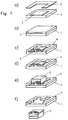
- Fig. 1 the method is shown schematically including various intermediate stages.
- a sacrificial layer 2 was applied to 300 nm thick gold via a mask 3, so that edge areas remained free on three sides of the substrate (step a)) .
- step b) a NiTi layer is applied over the entire surface Dusted substrate, with a central area of the layer over the sacrificial layer 2 and a peripheral area of the layer lie over the edge areas.
- the NiTi layer is then recrystallized in vacuo at 550 ° C for one hour.
- step c) the NiTi layer is electrolytically Structured photoetching. Doing so on this layer Paint either with the help of a dipping process or a spin process applied. The paint is then applied in the usual way exposed and developed, the exposed parts of the varnish be removed. Through the paint mask created with it selectively etched away the exposed parts of the NiTi layer and then the paint is completely removed. Part c) of Fig. 1 shows this state.
- the gold sacrificial layer 2 becomes selective detached. This gives you a cantilevered central area the NiTi layer, which is connected directly to the holding bars peripheral areas of the NiTi layer applied to the edge areas connected is.
- An aqueous was used as the etchant for gold Solution of 200 g / l potassium iodide and 100 g / l iodine used.
- an actuator housing is used as the second substrate 5 glued to the central area of the NiTi layer.
- the Housing 5 already contains a polyimide membrane (not shown), using the capillary adhesive technology with the central Area of the NiTi layer is connected.
- the housing 5 placed on the central area and then the glue dosed from the side to the adhesive gap. He pulls then due to capillary forces in the adhesive gap.
- the amount of adhesive can be the desired size of the adhesive surface can be set.
- step f) the housing 5 with the central one Area of the NiTi layer lifted off.
- the Holding bars are separated manually and then the housing from the substrate 1 removed.
- manual disconnection can be omitted, since here when removing of the housing 5 break the webs by themselves and the component release.
- the micromembrane actuator shows a micromembrane actuator produced using this technique, which are used for micropumps or micro valves can.
- the micromembrane actuator consists of a composite of one Housing 5 made of PMMA and a polyimide membrane 6, on one NiTi microstructure 7 is glued on.
- the microstructure corresponds the structured central area over the whole area microstructured NiTi layer applied to an auxiliary substrate.
Landscapes
- Engineering & Computer Science (AREA)
- Manufacturing & Machinery (AREA)
- Microelectronics & Electronic Packaging (AREA)
- Micromachines (AREA)
- Physical Vapour Deposition (AREA)
- Investigating Or Analyzing Materials By The Use Of Fluid Adsorption Or Reactions (AREA)
Applications Claiming Priority (2)
| Application Number | Priority Date | Filing Date | Title |
|---|---|---|---|
| DE19821841 | 1998-05-15 | ||
| DE1998121841 DE19821841C1 (de) | 1998-05-15 | 1998-05-15 | Verfahren zur Herstellung eines Bauteils, das eine Funktionsschicht enthält |
Publications (3)
| Publication Number | Publication Date |
|---|---|
| EP0957509A2 true EP0957509A2 (fr) | 1999-11-17 |
| EP0957509A3 EP0957509A3 (fr) | 2000-02-09 |
| EP0957509B1 EP0957509B1 (fr) | 2007-09-05 |
Family
ID=7867887
Family Applications (1)
| Application Number | Title | Priority Date | Filing Date |
|---|---|---|---|
| EP19990107921 Expired - Lifetime EP0957509B1 (fr) | 1998-05-15 | 1999-04-22 | Procédé de fabrication d'un composant comprenant une couche micro-structurée en alliage à mémoire de forme |
Country Status (2)
| Country | Link |
|---|---|
| EP (1) | EP0957509B1 (fr) |
| DE (2) | DE19821841C1 (fr) |
Cited By (4)
| Publication number | Priority date | Publication date | Assignee | Title |
|---|---|---|---|---|
| DE10042228A1 (de) * | 2000-08-28 | 2002-03-28 | Epcos Ag | Verfahren zur Beschichtung einer Vielzahl gleicher Grundkörper und Verwendung des Verfahrens |
| WO2007104444A1 (fr) * | 2006-03-14 | 2007-09-20 | Institut Für Mikroelektronik Stuttgart | Procédé pour produire un circuit intégré |
| DE102017102609A1 (de) | 2016-02-09 | 2017-08-10 | Comprisetec Gmbh | Verbindung von Bauteilen mittels Oberflächenstrukturen |
| DE102017115704A1 (de) | 2016-07-12 | 2018-04-12 | Comprisetec Gmbh | Bauteil zur reversiblen adhäsiven Anhaftung an einer glatten Fläche, Bausatz und Fertigungsverfahren |
Families Citing this family (3)
| Publication number | Priority date | Publication date | Assignee | Title |
|---|---|---|---|---|
| DE10321590B4 (de) * | 2003-05-14 | 2006-07-27 | Forschungszentrum Karlsruhe Gmbh | Verfahren zur Mikrostrukturierung von Pd-haltigen Funktionsschichten |
| DE102018112065A1 (de) | 2018-05-18 | 2019-11-21 | Memetis Gmbh | Ventil mit Aktuator aus einer Formgedächtnislegierung in flacher Geometrie |
| DE102019102908A1 (de) * | 2019-02-06 | 2020-08-06 | Fraunhofer-Gesellschaft zur Förderung der angewandten Forschung e.V. | Sensorvorrichtung für Druckmessungen von Fluiden, System für Druckmessungen von Fluiden |
Family Cites Families (1)
| Publication number | Priority date | Publication date | Assignee | Title |
|---|---|---|---|---|
| US4727047A (en) * | 1980-04-10 | 1988-02-23 | Massachusetts Institute Of Technology | Method of producing sheets of crystalline material |
-
1998
- 1998-05-15 DE DE1998121841 patent/DE19821841C1/de not_active Expired - Fee Related
-
1999
- 1999-04-22 DE DE59914487T patent/DE59914487D1/de not_active Expired - Lifetime
- 1999-04-22 EP EP19990107921 patent/EP0957509B1/fr not_active Expired - Lifetime
Cited By (6)
| Publication number | Priority date | Publication date | Assignee | Title |
|---|---|---|---|---|
| DE10042228A1 (de) * | 2000-08-28 | 2002-03-28 | Epcos Ag | Verfahren zur Beschichtung einer Vielzahl gleicher Grundkörper und Verwendung des Verfahrens |
| DE10042228C2 (de) * | 2000-08-28 | 2002-10-17 | Epcos Ag | Verfahren zur Beschichtung einer Vielzahl gleicher Grundkörper und Verwendung des Verfahrens |
| WO2007104444A1 (fr) * | 2006-03-14 | 2007-09-20 | Institut Für Mikroelektronik Stuttgart | Procédé pour produire un circuit intégré |
| US8466037B2 (en) | 2006-03-14 | 2013-06-18 | Institut Fuer Mikroelektronik Stuttgart | Method for producing a thin chip comprising an integrated circuit |
| DE102017102609A1 (de) | 2016-02-09 | 2017-08-10 | Comprisetec Gmbh | Verbindung von Bauteilen mittels Oberflächenstrukturen |
| DE102017115704A1 (de) | 2016-07-12 | 2018-04-12 | Comprisetec Gmbh | Bauteil zur reversiblen adhäsiven Anhaftung an einer glatten Fläche, Bausatz und Fertigungsverfahren |
Also Published As
| Publication number | Publication date |
|---|---|
| DE59914487D1 (de) | 2007-10-18 |
| EP0957509A3 (fr) | 2000-02-09 |
| EP0957509B1 (fr) | 2007-09-05 |
| DE19821841C1 (de) | 1999-06-24 |
Similar Documents
| Publication | Publication Date | Title |
|---|---|---|
| DE69512282T2 (de) | Herstellungsverfahren für ein mikromechanisches Element | |
| DE69933380T2 (de) | Verfahren zum hermetischen Einkapseln von Mikrosystemen vor Ort | |
| DE69634010T2 (de) | Ein verfahren zum herstellen von mikrogefertigten strukturen | |
| DE69313583T2 (de) | Methode zur Herstellung eines integrierten kapazitiven Transduktors | |
| DE69526557T2 (de) | Verfahren zur Herstellung einer Mikrostruktur | |
| DE2512086C3 (de) | Verfahren zur Herstellung freitragender, dünner Metallstrukturen | |
| DE69417725T2 (de) | Micro-bearbeitetes relais und verfahren zur herstellung des relais | |
| DE102005004878B4 (de) | Mikromechanischer kapazitiver Drucksensor und entsprechendes Herstellungsverfahren | |
| DE69015670T2 (de) | Herstellungsmethode für Halbleitermembranen. | |
| DE2901697C3 (de) | Verfahren zur Ausbildung von Leitungsverbindungen auf einem Substrat | |
| EP1167934A1 (fr) | Composant micromécanique, en particulier élément capteur, ayant une membrane stabilisée et procédé pour le produire | |
| EP0957509B1 (fr) | Procédé de fabrication d'un composant comprenant une couche micro-structurée en alliage à mémoire de forme | |
| DE4432725C1 (de) | Verfahren zur Herstellung eines dreidimensionalen Bauteils oder einer Bauteilgruppe | |
| EP0668995A1 (fr) | Procede de fabrication au moins une membrane montee sur un cadre | |
| DE19854803A1 (de) | Verfahren zur Herstellung einer lokal verstärkten metallischen Mikrostruktur | |
| DE60311504T2 (de) | Mikromechanisches relais mit anorganischer isolierung | |
| DE19600399C1 (de) | Herstellverfahren für ein mikromechanisches Bauteil mit einer beweglichen Struktur | |
| DE102014115243B4 (de) | Verfahren zur Herstellung von Dünnschichttransistoren zusammen mit anderen Bauelementen auf einem Substrat | |
| EP3665122B1 (fr) | Dispositif micromécanique et procédé de fabrication correspondant | |
| EP1238311B1 (fr) | Bobine plate et procede lithographique pour produire des microcomposants | |
| DE10333084A1 (de) | Thermogenerator und Verfahren zu dessen Herstellung | |
| EP0946792A1 (fr) | Element de construction micromecanique et procede de fabrication | |
| DE102015213714A1 (de) | Mikromechanisches Bauteil und Verfahren zur Herstellung eines piezoelektrischen mikromechanischen Bauteils | |
| DE2522944C3 (de) | Verfahren zur Herstellung einer elektrischen Dünnfilmschaltung | |
| DE102015102300A1 (de) | Verfahren zum Herstellen eines elektronischen Bauelements |
Legal Events
| Date | Code | Title | Description |
|---|---|---|---|
| PUAI | Public reference made under article 153(3) epc to a published international application that has entered the european phase |
Free format text: ORIGINAL CODE: 0009012 |
|
| AK | Designated contracting states |
Kind code of ref document: A2 Designated state(s): CH DE FR GB IT LI NL |
|
| AX | Request for extension of the european patent |
Free format text: AL;LT;LV;MK;RO;SI |
|
| PUAL | Search report despatched |
Free format text: ORIGINAL CODE: 0009013 |
|
| RIC1 | Information provided on ipc code assigned before grant |
Free format text: 7B 81C 1/00 A, 7B 81B 3/00 B, 7H 01L 21/306 B, 7H 01L 21/308 B |
|
| AK | Designated contracting states |
Kind code of ref document: A3 Designated state(s): AT BE CH CY DE DK ES FI FR GB GR IE IT LI LU MC NL PT SE |
|
| AX | Request for extension of the european patent |
Free format text: AL;LT;LV;MK;RO;SI |
|
| 17P | Request for examination filed |
Effective date: 20000122 |
|
| AKX | Designation fees paid |
Free format text: CH DE FR GB IT LI NL |
|
| GRAP | Despatch of communication of intention to grant a patent |
Free format text: ORIGINAL CODE: EPIDOSNIGR1 |
|
| RTI1 | Title (correction) |
Free format text: METHOD OF MANUFACTURING A DEVICE COMPRISING A MICRO-STRUCTURED LAYER OF SHAPE MEMORY ALLOY |
|
| GRAS | Grant fee paid |
Free format text: ORIGINAL CODE: EPIDOSNIGR3 |
|
| GRAA | (expected) grant |
Free format text: ORIGINAL CODE: 0009210 |
|
| AK | Designated contracting states |
Kind code of ref document: B1 Designated state(s): CH DE FR GB IT LI NL |
|
| REG | Reference to a national code |
Ref country code: GB Ref legal event code: FG4D Free format text: NOT ENGLISH |
|
| REG | Reference to a national code |
Ref country code: CH Ref legal event code: NV Representative=s name: ROTTMANN, ZIMMERMANN + PARTNER AG Ref country code: CH Ref legal event code: EP |
|
| REF | Corresponds to: |
Ref document number: 59914487 Country of ref document: DE Date of ref document: 20071018 Kind code of ref document: P |
|
| GBT | Gb: translation of ep patent filed (gb section 77(6)(a)/1977) |
Effective date: 20071122 |
|
| EN | Fr: translation not filed | ||
| ET | Fr: translation filed | ||
| PLBE | No opposition filed within time limit |
Free format text: ORIGINAL CODE: 0009261 |
|
| REG | Reference to a national code |
Ref country code: FR Ref legal event code: EERR Free format text: CORRECTION DE BOPI 08/18 - BREVETS EUROPEENS DONT LA TRADUCTION N A PAS ETE REMISE A L INPI. IL Y A LIEU DE SUPPRIMER : LA MENTION DE LA NON-REMISE. LA REMISE DE LA TRADUCTION EST PUBLIEE DANS LE PRESENT BOPI. |
|
| STAA | Information on the status of an ep patent application or granted ep patent |
Free format text: STATUS: NO OPPOSITION FILED WITHIN TIME LIMIT |
|
| 26N | No opposition filed |
Effective date: 20080606 |
|
| PG25 | Lapsed in a contracting state [announced via postgrant information from national office to epo] |
Ref country code: FR Free format text: LAPSE BECAUSE OF FAILURE TO SUBMIT A TRANSLATION OF THE DESCRIPTION OR TO PAY THE FEE WITHIN THE PRESCRIBED TIME-LIMIT Effective date: 20080502 |
|
| PGFP | Annual fee paid to national office [announced via postgrant information from national office to epo] |
Ref country code: FR Payment date: 20110427 Year of fee payment: 13 Ref country code: CH Payment date: 20110421 Year of fee payment: 13 |
|
| PGFP | Annual fee paid to national office [announced via postgrant information from national office to epo] |
Ref country code: NL Payment date: 20110420 Year of fee payment: 13 Ref country code: GB Payment date: 20110419 Year of fee payment: 13 |
|
| REG | Reference to a national code |
Ref country code: CH Ref legal event code: PFA Owner name: FORSCHUNGSZENTRUM KARLSRUHE GMBH Free format text: FORSCHUNGSZENTRUM KARLSRUHE GMBH#WEBERSTRASSE 5#76133 KARLSRUHE (DE) -TRANSFER TO- FORSCHUNGSZENTRUM KARLSRUHE GMBH#WEBERSTRASSE 5#76133 KARLSRUHE (DE) |
|
| PGFP | Annual fee paid to national office [announced via postgrant information from national office to epo] |
Ref country code: IT Payment date: 20110427 Year of fee payment: 13 |
|
| PGFP | Annual fee paid to national office [announced via postgrant information from national office to epo] |
Ref country code: DE Payment date: 20110620 Year of fee payment: 13 |
|
| REG | Reference to a national code |
Ref country code: NL Ref legal event code: V1 Effective date: 20121101 |
|
| REG | Reference to a national code |
Ref country code: CH Ref legal event code: PL |
|
| GBPC | Gb: european patent ceased through non-payment of renewal fee |
Effective date: 20120422 |
|
| REG | Reference to a national code |
Ref country code: FR Ref legal event code: ST Effective date: 20121228 |
|
| PG25 | Lapsed in a contracting state [announced via postgrant information from national office to epo] |
Ref country code: LI Free format text: LAPSE BECAUSE OF NON-PAYMENT OF DUE FEES Effective date: 20120430 Ref country code: GB Free format text: LAPSE BECAUSE OF NON-PAYMENT OF DUE FEES Effective date: 20120422 Ref country code: CH Free format text: LAPSE BECAUSE OF NON-PAYMENT OF DUE FEES Effective date: 20120430 |
|
| REG | Reference to a national code |
Ref country code: DE Ref legal event code: R119 Ref document number: 59914487 Country of ref document: DE Effective date: 20121101 |
|
| PG25 | Lapsed in a contracting state [announced via postgrant information from national office to epo] |
Ref country code: FR Free format text: LAPSE BECAUSE OF NON-PAYMENT OF DUE FEES Effective date: 20120430 Ref country code: IT Free format text: LAPSE BECAUSE OF NON-PAYMENT OF DUE FEES Effective date: 20120422 |
|
| PG25 | Lapsed in a contracting state [announced via postgrant information from national office to epo] |
Ref country code: NL Free format text: LAPSE BECAUSE OF NON-PAYMENT OF DUE FEES Effective date: 20121101 |
|
| PG25 | Lapsed in a contracting state [announced via postgrant information from national office to epo] |
Ref country code: DE Free format text: LAPSE BECAUSE OF NON-PAYMENT OF DUE FEES Effective date: 20121101 |