EP0959595A2 - Dispositif d'émission et système de bus pour transmission de données - Google Patents
Dispositif d'émission et système de bus pour transmission de données Download PDFInfo
- Publication number
- EP0959595A2 EP0959595A2 EP99109758A EP99109758A EP0959595A2 EP 0959595 A2 EP0959595 A2 EP 0959595A2 EP 99109758 A EP99109758 A EP 99109758A EP 99109758 A EP99109758 A EP 99109758A EP 0959595 A2 EP0959595 A2 EP 0959595A2
- Authority
- EP
- European Patent Office
- Prior art keywords
- signal
- bus
- converter
- transmitting
- bus system
- Prior art date
- Legal status (The legal status is an assumption and is not a legal conclusion. Google has not performed a legal analysis and makes no representation as to the accuracy of the status listed.)
- Withdrawn
Links
- 230000005540 biological transmission Effects 0.000 title claims description 19
- 230000000630 rising effect Effects 0.000 claims abstract description 7
- 238000004891 communication Methods 0.000 claims description 16
- 238000012546 transfer Methods 0.000 claims description 12
- 238000009499 grossing Methods 0.000 claims description 9
- 230000003321 amplification Effects 0.000 claims description 6
- 238000003199 nucleic acid amplification method Methods 0.000 claims description 6
- 239000004065 semiconductor Substances 0.000 claims description 6
- 230000001174 ascending effect Effects 0.000 claims description 4
- 230000001105 regulatory effect Effects 0.000 claims description 3
- 230000001276 controlling effect Effects 0.000 claims 1
- 230000005670 electromagnetic radiation Effects 0.000 description 15
- 230000006870 function Effects 0.000 description 9
- 238000010586 diagram Methods 0.000 description 5
- 238000011144 upstream manufacturing Methods 0.000 description 4
- 230000005855 radiation Effects 0.000 description 3
- 238000001228 spectrum Methods 0.000 description 3
- 230000009467 reduction Effects 0.000 description 2
- 230000008901 benefit Effects 0.000 description 1
- 230000008859 change Effects 0.000 description 1
- 230000009849 deactivation Effects 0.000 description 1
- 238000011161 development Methods 0.000 description 1
- 230000018109 developmental process Effects 0.000 description 1
- 238000009434 installation Methods 0.000 description 1
- 238000000034 method Methods 0.000 description 1
- 238000012986 modification Methods 0.000 description 1
- 230000004048 modification Effects 0.000 description 1
- 238000005457 optimization Methods 0.000 description 1
- 230000008569 process Effects 0.000 description 1
- 230000000750 progressive effect Effects 0.000 description 1
- 230000001681 protective effect Effects 0.000 description 1
- 230000003595 spectral effect Effects 0.000 description 1
Images

Classifications
-
- H—ELECTRICITY
- H04—ELECTRIC COMMUNICATION TECHNIQUE
- H04L—TRANSMISSION OF DIGITAL INFORMATION, e.g. TELEGRAPHIC COMMUNICATION
- H04L25/00—Baseband systems
- H04L25/02—Details ; arrangements for supplying electrical power along data transmission lines
- H04L25/03—Shaping networks in transmitter or receiver, e.g. adaptive shaping networks
- H04L25/03828—Arrangements for spectral shaping; Arrangements for providing signals with specified spectral properties
- H04L25/03834—Arrangements for spectral shaping; Arrangements for providing signals with specified spectral properties using pulse shaping
-
- H—ELECTRICITY
- H04—ELECTRIC COMMUNICATION TECHNIQUE
- H04L—TRANSMISSION OF DIGITAL INFORMATION, e.g. TELEGRAPHIC COMMUNICATION
- H04L25/00—Baseband systems
- H04L25/02—Details ; arrangements for supplying electrical power along data transmission lines
- H04L25/0264—Arrangements for coupling to transmission lines
- H04L25/028—Arrangements specific to the transmitter end
- H04L25/0286—Provision of wave shaping within the driver
Definitions
- the invention relates to a transmission device and a bus system for serial data transmission of binary data between at least two communication stations that have one individual bus line are coupled together.
- a suitable bus system can be, for example, a CAN bus system (Controller Area Network).
- CAN bus system Controller Area Network
- Such a CAN bus system is described for example in DE 195 230 31 A1.
- the transmission device of this transceiver circuit can be essential Influence on the edge shape of the to be coupled into the bus Signal.
- the frequency spectrum is broadening electromagnetic radiation, if the Edge steepness of those coupled into the bus system Bus signals increases.
- EMC electromagnetic compatibility
- bus system For cost reasons, it is often cheaper to use a bus system to use only a single bus line.
- the bus system is, for example, the single-wire CAN bus (single wire CAN bus).
- single-wire CAN bus single wire CAN bus
- Such one-wire buses have the Disadvantage that the electromagnetic radiation is not as with two-wire or multi-wire bus systems by twisting can be compensated.
- bus systems are connected to passive components. This measure improves the electromagnetic radiation however insufficient and also reduces the bandwidth of the Bus system.
- this task is performed by a bus system type mentioned solved in that the transmitting device has a circuit for edge shape adjustment, the generates an output signal from a data signal to be sent, its rising and falling flanks on the curve are approximated to a sine function, each time one of the edges to the rising sine half wave and the each other edge approximates the falling sine half-wave is.
- Such output signals with edges in the form of a Half-sine waves have a particularly low harmonic content on, theoretically only the fundamental wave.
- a circuit according to the invention for flank shape adjustment advantageously at one One-wire bus system the radiation or the radiation of unwanted electromagnetic radiation to a minimum to reduce.
- edges of the output signals to be transmitted via the bus are supposed to approximate the shape of a sinusoidal function become.
- the ascending flank becomes the ascending flank Sinusoidal half wave and for the falling edge in each case reproduced the falling sine half-wave.
- In the negative Logic creates a rising edge a falling edge Sine half-wave, while a falling edge is one ascending sine half-wave generated.
- the area of the sinusoidal wave between its minimum and maximum is to be understood as the rising sine half-wave.
- the falling sine half-wave is the area of the sinusoidal wave between its maximum and its minimum.
- Any function derived from a sine function or from a cosine function is to be understood as a sinusoidal function. It is particularly advantageous if function (cosx) 2 is selected as the sinusoidal function.
- the circuit for edge shape adjustment is connected in series Clock generation device, counter device and converter device.
- the typically as an Osillator trained clock generator device generates a clock signal.
- the downstream clock-controlled counter device for example an up-down counter, counts continuously the coupled clock pulses of the oscillator and leads a derived from the number of coupled clock pulses Counter status signal of the downstream converter device to.
- the converter device which is usually a digital-to-analog converter (DA converter) is generated based on the meter reading signal an analog signal with step-shaped clock edges.
- DA converter digital-to-analog converter
- step-shaped clock edges in the analog signal are sinusoidal It reproduces half-wave as optimally as possible necessary that the individual stages if possible not the same Have step height.
- the optimal setting of each Step heights and thus the optimization of the sinusoidal Half-wave of the clock edges can be made using a suitable one Dimensioning of the reference elements of the voltage divider of the DA converter.
- This DA converter has a voltage divider with a variety of reference resistors on which on the input side the respective counter reading of the upstream Counter device is supplied.
- the reference resistors are to be set so that the output values of the D / A converter the corresponding discrete value on the sinusoidal Half wave corresponds.
- the step heights of the Remove the analog signal should gradually increase. From the middle of the meter reading, the step heights of the Remove the analog signal accordingly. So you can about the dimensioning of the reference resistors on simple To simulate the sinusoidal half-wave.
- a load resistor with switchable, controllable current sources conceivable.
- the reference elements are then through Current sources, for example as controllable transistors form a diode network.
- the dimensioning of the Reference elements and thus the generation of the optimal step heights in the output signal of the DA converter could then over the W / L ratios of the transistors take place.
- step-shaped Analog signal having clock edges a smoothing filter, in particular a low-pass filter becomes.
- a smoothing filter By means of suitable dimensioning of the filter elements the levels in the clock edges of the analog signal filter out. A continuous, analogue then arises Output signal that optimal to the sinusoidal half wave is approximated.
- the DA converter or the smoothing filter downstream an amplifier device with feedback branch.
- the amplifier device preferably as an analog Operational amplifier is designed, amplifies that output signal to be driven on the bus with a suitable amplification.
- the so-called Wake-up mode can be used to create a so-called wake-up signal impress on the bus line. Compared to the normal signal has this wake-up signal according to the gain a significantly increased amplitude. With this wake-up signal all network nodes on the bus system, that were previously in so-called sleep mode and then selectively activated or back into the Sleep mode controlled.
- the wake-up mode is advantageously used the average current consumption of a bus system significantly reduced since all "sleeping" network nodes that are not addressed during a bus transfer, in the power-saving sleep mode persist.
- the clock generating device or the oscillator in their working frequency adjustable is.
- This is an adjustable resistance of the clock generating device upstream. This allows the oscillator frequency and thus the average slope of the clock edge of the output signal to the desired data transfer rate to adjust.
- the adjustable Resistance which is usually external thus a more or less high data transfer rate of the bus system.
- the Voltage regulating device and the transmitter / receiver device assigned to it a communication station on one single semiconductor chip are integrated monolithically.
- these voltage regulator modules and the transceiver integrated monolithically because the technological Requirements of these modules are very similar.
- the microcontroller along with the one assigned to it Voltage regulating device and transmitting / receiving device also are monolithically integrated on the same semiconductor chip.
- the circuit for flank shape adjustment according to the invention signals to be sent is typically in a transmitting device integrated into a communication station. Especially This transmission device according to the invention is advantageous in a bus system for data transmission.
- the invention is particularly suitable in the automotive field in so-called CAN electrical system.
- a microprocessor controls via an internal bus and a so-called CAN module, which contains the corresponding CAN protocol, via the transceiver circuit transfers data over the one-wire bus.
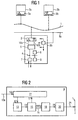
- Figure 1 shows a one-wire bus system for serial transmission of binary data between connected to the bus State-of-the-art communication stations. It will subsequently assumed that the bus system is a so-called CAN bus system (Controller Area Network). Farther it is assumed that a so-called single-wire bus or single-wire bus (SW bus) with a single one Transmission line is provided.
- CAN bus system Controller Area Network
- 1 is the (only) bus line of the bus system designated.
- the bus system has a large number of communication stations 2, 2a, 2b, which are also referred to as network nodes be on.
- the network node 2 consists of a physical transceiver 3.
- the transceiver 3 or the transceiver forms the interface of the network node 2 to bus 1.
- the network node points 2 between an internal bus 4 and the transceiver 3 switched communication interface 5 on a Connection line 10a, 10b connected to the transceiver 3 is.
- the connecting line is 10a with the transmitter and the connecting line 10b with the receiving device of the transceiver 3 connected.
- the communication module 5 is often called CAN module designates and controls according to the CAN protocol data transfer via the bus.
- the network node 2 also has a microprocessor 6, an I / O device 7 and a memory unit 8, which are each coupled to the internal bus 4. Especially It is advantageous, as shown in Figure 1, if the elements 3 to 8 of a network node 2 on a single one Semiconductor chip are integrated monolithically. This is particularly so for cost reasons due to the smaller space requirement advantageous.
- a voltage supply line 8a is also provided Power supply provided.
- the power supply line 8a is typically in the communication device 2 provided voltage control module 8b connected.
- the voltage control module 8b thus draws its supply voltage via the voltage supply line 8a and the supply voltage for all modules of the network node mentioned so far 2 ready. Because the requirements are high currents and high voltages from both the transceiver 3 and the Voltage control module 8b must be met, in particular these modules are advantageously monolithic on one integrated single semiconductor chip.
- three network nodes 2, 2a, 2b are on the bus 1 connected.
- the network node 2 as mentioned above, a transceiver 3, which is both for Sending as well as receiving data is suitable.
- the associated one Network node 2 works as a master-slave unit.
- the network node 2a has a transceiver 3a, which has only one receiving device and is therefore only suitable for receiving data (Receiver).
- the associated network node 2a is therefore one Slave unit.
- the network node 2b has a transceiver 3b, which is designed as a transmitting device and therefore is used exclusively for sending data (transmitter).
- the associated network node 2b is thus a master unit.
- a CAN bus system described above, which instead of a single Bus line is equipped with two bus lines is in Wolfhard Lawrenz (ed.), CAN - Controller Area Network, Fundamentals and practice, Wegig-Verlag, 1997, page 3 ff.
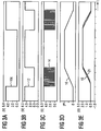
- Figure 2 shows the block diagram of an inventive Circuit for edge shape adjustment for a transmitter of a one-wire bus system.
- the block diagram in Figure 2 only for sending data signals necessary elements.
- 9 is a circuit for edge shape adjustment designated.
- the edge shape adjustment circuit 9 is here between the connecting line 10a and the bus 1 switched.
- the control device 11 generates a control signal 12 that is input to a clock generator 13 is coupled.
- the clock generating device 13, which is typically designed as an oscillator a clock signal 14 at its output, which is connected downstream Counter device 15 is supplied.
- the counter device 15 is in the present example as a 4-bit up-down counter educated.
- the counter device 15 determines clock-controlled depending on the number of injected Cycles of the clock signal 14 each have a counter reading which Counter status signal 16 can be tapped at the output of the counter device 15 is.
- the counter device 15 generates a control signal 17 which feeds back into the control device 11 becomes.
- the counter reading 16 of the counter device 15 is connected downstream Transducer device 18 supplied.
- the exemplary embodiment is the converter device 18 as a digital-to-analog converter (DA converter) trained.
- the converter device 18 generates an analog signal 19 on the output side step-shaped signal edges, which has a smoothing filter 20, for example a low-pass filter.
- the smoothing filter 20 generates an optimized with regard to the shape of the clock edges
- Output signal 21, which is the output of the circuit 9 can be coupled into the bus 1.
- With low bus impedance is an amplifier between the circuit 9 and the bus 1 required as an impedance converter.
- a negative edge (H-L) of the data signal 10c to be sent causes the oscillator 13 by the control signal 12 ( Figure 3 (b)) is started.
- the output side of Oscillator 13 generated clock pulses 14 ( Figure 3 (c)) counted continuously by the up-down counter 15.
- the downstream DA converter 18 has an analog signal 19 generated with step-shaped signal edges (Fig 3 (e)), which corresponds to the respective counter position of the counter 15.
- the analog signal 19 is used to smooth the steps a downstream low-pass filter 20 supplied.
- an output signal 21 (FIG 3 (e)) tapped, the clock edge in the form of sine half-waves having.
- the output signal 21 thus corresponds to one potential given by the converter device 18, the was additionally smoothed.
- the counter device 15 Generated after a predetermined number of clock pulses 14 the counter device 15 a control signal 17, which is in the control device 11 is fed back.
- the control device 11 stops the oscillator via the control signal 12 (FIG. 3 (b)) 13.
- This number of bars typically corresponds to the number of the voltage values that the DA converter 18 can output.
- the oscillator 13 is thus stopped after a maximum of 16 clock periods.
- the counter device 15 thus preferably has the same data depth as the digital-to-analog converter 18th
- a DA converter 18 is advantageously an after DA converter 18 operating in parallel is used.
- Means a suitable dimensioning of the voltage divider of the parallel DA converter 18 are the voltage values of the DA converter 18 each assigned individual converter steps.
- the means the level of the individual stages of the analog signal 19 can be specifically adjusted in this way. So you can due to suitably set reference resistances of the DA converter 18 the edge shape of the output signal 21, such optimize that these correspond to the shape of a sine half-wave Because signals whose edges are in the form of a sine half-wave have a particularly low harmonic content, namely theoretically only the fundamental wave, cause such Output signals 21 on the bus line 1 a minimum or no EMC radiation at all.
- any other DA converter would also be used as converter device 18 18 conceivable.
- the converter device 18 through a load resistor with switchable, controllable power sources can be realized.
- the controllable Current sources could be transistors, for example can be controlled via a logic circuit be.
- Such a diode network also provides one Current with step-shaped edges, however, is circuit-technical more complex than the parallel DA converter described above.
- Figure 4 shows a preferred embodiment of a transceiver circuit for a one-wire bus system, the one according to the invention Circuit for edge shape adjustment accordingly Figure 2 has.
- the circuit for setting the edge shape 9 is preceded by a time-out circuit 30, to which the data signal 10c to be transmitted is fed and which drives the downstream circuit 9.
- a control logic circuit 32 is also provided, to which a first control signal 31 is supplied. In the present case, it is a 2-bit control signal. The control logic circuit 32 then generates a second control signal 32a, which is fed to the time-out circuit 30 and the circuit 9.
- an amplifier device 33 may be connected between the circuit to 9 and bus 1 between the circuit to 9 and bus 1 .
- the exemplary embodiment comprises the amplifier device 33 an analog operational amplifier 34 with negative feedback branch 35.
- the second is also in the negative feedback branch 35 Control signal 32a of the control logic circuit 32 coupled.
- the amplifier device 33 is used here to amplify the Output signal 21 to be impressed on bus 1.
- amplifiers 33 are for generating one Output signals 21, 22 with sinusoidal half-wave edges not mandatory.
- the smoothing filter 20 in particular in the case of a DA converter 18, which has a low Bit width has a great advantage, because it sometimes relatively large steps of the edges of the analog signal 19 largely filtered out. In this way significantly reduce EMC emissions.
- a further control signal 37 can be coupled into the oscillator 13 of the circuit for edge shape adjustment 9.
- this resistor 36 which is typically designed externally, the working frequency and thus the average slope of the clock edges of the output signal 21, 22 can be adapted to the desired data transmission rate.
- a more or less high data transmission rate of the bus system can thus be achieved.
- a line terminating resistor 38 is provided as a load for the amplification device 33.
- the line termination is designed as a high-side switch.
- the base point or the ground potential V GND of the line terminating resistor 38 is connected in parallel via a load base point driver 39 from the output 41 of the transceiver circuit 3 of the bus line 1.
- the load base point driver 39 is a low-side driver, which connects the line terminating resistor 38 to the potential of the reference ground V GND .
- a protective circuit 40 is provided for the load foot point driver 39. This switches off the load foot point driver 39 when the difference in the battery potential and the potential of the reference ground (V BAT -V GND ) decrease. This can occur, for example, in the event of a short-circuit of the supply voltage V BAT to the reference potential V GND or, for example, if the contact of the network node 2 with the potential of the reference ground V GND is cut off or becomes more high-resistance (so-called lost-off ground). This deactivation means that the bus line 1 can never be influenced or even blocked via a raised ground potential V GND in the network.
- the transceiver circuit 3 in Figure 4 has next to the device a device for transmitting a data signal 10c for receiving data signals coupled from bus 1 42 on.
- the output 41 of the transceiver circuit 3 serves a one-wire bus system therefore also as an input.
- a bus 1 is coupled in via the output / input 41 Data signal 42 via an input filter 43 and via an amplification device 44 coupled into the transceiver circuit 3.
- Input filter 43 and amplification device 44 thus form the receiving device of the transceiver circuit 3.
- the filtered and amplified coupled binary data signal 10d can be received by a downstream microprocessor 6 can be tapped.
- the Control logic circuit 32 uses the Control signal 32a the operating mode of the transceiver circuit 3 firm. For example, with a 2-bit control signal 31 maximum 4 different operating modes can be set.
- the following Operating modes can be provided:
- the transceiver circuit sends 3 data signals over the bus with a relatively low transfer rate of typically 25 Kbit / sec.
- the circuit for edge shape adjustment 9 is common in this mode of operation activated.
- a network node 2 At a network node 2 is the corresponding transceiver circuit 3 disabled, i. H. it is not a data transfer to Bus 1 provided, then the transceiver circuit 3 in controlled the sleep mode. The corresponding has in sleep mode Network node 2 then has a very low power consumption.
- the circuit for edge shape adjustment is in wake-up mode 9 activated.
- by a corresponding Control of the feedback branch 35 of the amplifier device 33 increases the amplification of the output signal 21.
- On the bus line 1 thereby becomes a so-called wake-up signal embossed. Compared to the normal signal, this has a wake-up signal a significantly increased amplitude.
- the wake-up signal a master unit, all network nodes 2 on Bus system "woken up” and then selectively activated or switched back to sleep mode. Using this wake-up mode the average current consumption of a bus system becomes clear reduced since all "sleeping" network nodes 2 that are not addressed during a bus transfer, in the Persist in sleep mode.
- the receiving device 43, 44, 10b gives a data packet 42 coming from the bus 1 during sleep mode only then to the downstream microcontroller 6 continue if they have the for a defined minimum time Compared to the normal level, the wake-up voltage level is significantly higher has identified.
- one of the receiving devices occurs during sleep mode 43, 44, 10b registered change in data transfer on bus line 1, then it will be in sleep mode located transceiver circuit 3 or the corresponding Network node 2 woken up again and in the operating state, that means normal operation or high-speed mode, or the Controlled wake-up mode.
- the time-out circuit 30 can be the transceiver circuit 3 switch off in case the one to be sent Data signal 10c for a predetermined period of time, for example a few milliseconds, has not changed. This is particularly advantageous if, for example, the upstream Microprocessor 6 permanently due to an error sends an active data signal.
- the bus 1 can then also permanently through the corresponding network node 2 be blocked because the dominant level can never be blocked by others Network nodes are overwritten. This allows the other network nodes 2 connected to bus 1 no data receive or send more. Bus 1 is thus blocked.
- the time-out circuit 30 is used the corresponding network node 2 according to a predetermined Time decoupled from bus 1 via a time-out signal.
- the invention is particularly advantageous in automotive electronics in an electrical system such as one CAN bus system.
Landscapes
- Engineering & Computer Science (AREA)
- Physics & Mathematics (AREA)
- Spectroscopy & Molecular Physics (AREA)
- Power Engineering (AREA)
- Computer Networks & Wireless Communication (AREA)
- Signal Processing (AREA)
- Dc Digital Transmission (AREA)
- Small-Scale Networks (AREA)
Applications Claiming Priority (2)
| Application Number | Priority Date | Filing Date | Title |
|---|---|---|---|
| DE19822259A DE19822259C2 (de) | 1998-05-18 | 1998-05-18 | Sendeeinrichtung und Bussystem zur Datenübertragung |
| DE19822259 | 1998-05-18 |
Publications (2)
| Publication Number | Publication Date |
|---|---|
| EP0959595A2 true EP0959595A2 (fr) | 1999-11-24 |
| EP0959595A3 EP0959595A3 (fr) | 2003-08-06 |
Family
ID=7868168
Family Applications (1)
| Application Number | Title | Priority Date | Filing Date |
|---|---|---|---|
| EP99109758A Withdrawn EP0959595A3 (fr) | 1998-05-18 | 1999-05-18 | Dispositif d'émission et système de bus pour transmission de données |
Country Status (3)
| Country | Link |
|---|---|
| US (1) | US6484223B1 (fr) |
| EP (1) | EP0959595A3 (fr) |
| DE (1) | DE19822259C2 (fr) |
Cited By (4)
| Publication number | Priority date | Publication date | Assignee | Title |
|---|---|---|---|---|
| WO2013113570A1 (fr) * | 2012-02-03 | 2013-08-08 | Robert Bosch Gmbh | Dispositif récepteur pour un appareil de commande situé dans un véhicule et procédé pour générer une impulsion de synchronisation |
| WO2013117415A1 (fr) * | 2012-02-06 | 2013-08-15 | Robert Bosch Gmbh | Dispositif et procédé de génération d'une impulsion de synchronisation sensiblement sinusoïdale |
| CN104871475A (zh) * | 2012-12-27 | 2015-08-26 | 罗伯特·博世有限公司 | 用于车辆中的控制装置的接收装置及用于产生同步脉冲的方法 |
| CN108010537A (zh) * | 2017-12-30 | 2018-05-08 | 长沙迪普美医疗科技有限公司 | 一种声音报警处理方法、装置、系统 |
Families Citing this family (21)
| Publication number | Priority date | Publication date | Assignee | Title |
|---|---|---|---|---|
| US6760801B1 (en) * | 2001-03-06 | 2004-07-06 | Intel Corporation | Ground referenced voltage source input/output scheme for multi-drop bus |
| CN1659066A (zh) * | 2002-06-10 | 2005-08-24 | 皇家飞利浦电子股份有限公司 | 在子网运行和总网运行之间切换的方法和系统 |
| DE10349600B4 (de) * | 2002-10-25 | 2011-03-03 | Infineon Technologies Ag | Verfahren zur Überprüfung von Leitungsfehlern in einem Bussystem und Bussystem |
| DE102004002771A1 (de) * | 2004-01-20 | 2005-08-11 | Daimlerchrysler Ag | Verfahren und Vorrichtung zur Bewertung von Einstellungen eines CAN-Geräts |
| US8046488B2 (en) * | 2004-05-21 | 2011-10-25 | Intel Corporation | Dynamically modulating link width |
| US20080198908A1 (en) * | 2005-06-09 | 2008-08-21 | Nxp B.V. | Transceiver |
| US7694060B2 (en) * | 2005-06-17 | 2010-04-06 | Intel Corporation | Systems with variable link widths based on estimated activity levels |
| DE102009054168A1 (de) * | 2009-11-23 | 2011-05-26 | Marquardt Gmbh | Schnittstelle für Datenübertragung |
| GB2492389A (en) | 2011-06-30 | 2013-01-02 | Tomtom Int Bv | Pulse shaping is used to modify a timing signal prior to propagation to reduce electromagnetic radiation |
| US8868955B2 (en) | 2011-07-01 | 2014-10-21 | Intel Corporation | Enhanced interconnect link width modulation for power savings |
| US9053244B2 (en) | 2012-06-28 | 2015-06-09 | Intel Corporation | Utilization-aware low-overhead link-width modulation for power reduction in interconnects |
| US9183171B2 (en) | 2012-09-29 | 2015-11-10 | Intel Corporation | Fast deskew when exiting low-power partial-width high speed link state |
| DE102013020663B4 (de) | 2013-12-06 | 2020-08-06 | Elmos Semiconductor Aktiengesellschaft | Vorrichtung und Verfahren zur Slew-Rate-Generierung für LIN-Bus-Treiber |
| DE102013226300B4 (de) * | 2013-12-17 | 2026-03-19 | Robert Bosch Gmbh | Verfahren zum Erzeugen eines Pulses und Schaltungseinrichtung für ein elektronisches Gerät zur Erzeugung eines Pulses |
| RU2653306C1 (ru) | 2014-03-20 | 2018-05-07 | Интел Корпорейшн | Способ, устройство и система для управления потреблением энергии неиспользуемым аппаратным средством канального интерфейса |
| JP6450212B2 (ja) | 2015-02-10 | 2019-01-09 | ルネサスエレクトロニクス株式会社 | 電流出力回路 |
| JP6520414B2 (ja) * | 2015-06-02 | 2019-05-29 | 株式会社デンソー | 流量測定装置 |
| DE102015222334A1 (de) * | 2015-11-12 | 2017-05-18 | Robert Bosch Gmbh | Einrichtung und Verfahren zum selektiven Ausblenden von Busschwingungen beim Datenempfang über ein Bussystem |
| US10812051B2 (en) * | 2017-08-23 | 2020-10-20 | Maxlinear, Inc. | Method and system for a matching circuit for a broadband bus in automotive applications |
| DE102018203708A1 (de) * | 2018-03-12 | 2019-09-12 | Robert Bosch Gmbh | Sende-/Empfangseinrichtung für ein Bussystem und Betriebsverfahren hierfür |
| CN114401161B (zh) * | 2021-12-21 | 2023-08-11 | 珠海格力电器股份有限公司 | 基于二总线的通讯优化设备、方法和通讯系统 |
Family Cites Families (15)
| Publication number | Priority date | Publication date | Assignee | Title |
|---|---|---|---|---|
| US3134098A (en) * | 1960-02-04 | 1964-05-19 | Sperry Gyroscope Company Of Ca | Digital-to-analog converter |
| US3701144A (en) * | 1970-10-28 | 1972-10-24 | Us Navy | High frequency analog-to-digital converter |
| DE2359953C3 (de) * | 1973-12-03 | 1979-03-01 | Siemens Ag, 1000 Berlin Und 8000 Muenchen | Schaltungsanordnung zur Umsetzung digitaler in analoge Sinus- und/oder Cosinuswinkelwerte |
| DE2821023B2 (de) * | 1978-05-12 | 1980-07-24 | Institut Fuer Rundfunktechnik Gmbh, 8000 Muenchen | Schaltungsanordnung zum Erzeugen eines Ausgangssignals |
| US4311921A (en) * | 1979-04-09 | 1982-01-19 | The Grass Valley Group, Inc. | Sine-squared pulse shaping circuit |
| US4410955A (en) * | 1981-03-30 | 1983-10-18 | Motorola, Inc. | Method and apparatus for digital shaping of a digital data stream |
| JPS59141805A (ja) * | 1983-02-02 | 1984-08-14 | Fujitsu Ten Ltd | 繰り返し波形発生回路 |
| US4593206A (en) * | 1984-01-16 | 1986-06-03 | Motorola, Inc. | Fixed slew rate bus driver circuit |
| US4611101A (en) * | 1984-08-29 | 1986-09-09 | Tii Computer Systems, Inc. | Method and apparatus for testing communication systems |
| AU608822B2 (en) * | 1987-06-29 | 1991-04-18 | Digital Equipment Corporation | Bus transmitter having controlled trapezoidal slew rate |
| US5164611A (en) * | 1990-10-18 | 1992-11-17 | Delco Electronics Corporation | Low noise communication bus driver |
| US5410188A (en) * | 1992-12-22 | 1995-04-25 | National Semiconductor Corporation | Enhanced integrated waveshaping circuit |
| US5408497A (en) * | 1993-07-14 | 1995-04-18 | Echelon Corporation | Transceiver for transmitting and receiving stair-stepped sinusoidal waveforms |
| US5732106A (en) * | 1995-06-05 | 1998-03-24 | Itt Corporation | Pulse-shaping filter for modulator monolithic integration |
| DE19523031A1 (de) * | 1995-06-08 | 1996-12-12 | Philips Patentverwaltung | System zum Übertragen von Daten über einen differentiellen Bus |
-
1998
- 1998-05-18 DE DE19822259A patent/DE19822259C2/de not_active Expired - Fee Related
-
1999
- 1999-05-18 US US09/313,894 patent/US6484223B1/en not_active Expired - Lifetime
- 1999-05-18 EP EP99109758A patent/EP0959595A3/fr not_active Withdrawn
Cited By (10)
| Publication number | Priority date | Publication date | Assignee | Title |
|---|---|---|---|---|
| WO2013113570A1 (fr) * | 2012-02-03 | 2013-08-08 | Robert Bosch Gmbh | Dispositif récepteur pour un appareil de commande situé dans un véhicule et procédé pour générer une impulsion de synchronisation |
| KR20140121829A (ko) * | 2012-02-03 | 2014-10-16 | 로베르트 보쉬 게엠베하 | 차량 내 제어 장치용 수신 어셈블리 및 동기화 펄스를 발생시키기 위한 방법 |
| US9937886B2 (en) | 2012-02-03 | 2018-04-10 | Robert Bosch Gmbh | Receiver configuration for a control unit in a vehicle and method for generating a synchronization pulse |
| KR101998908B1 (ko) | 2012-02-03 | 2019-07-10 | 로베르트 보쉬 게엠베하 | 차량 내 제어 장치용 수신 어셈블리 및 동기화 펄스를 발생시키기 위한 방법 |
| WO2013117415A1 (fr) * | 2012-02-06 | 2013-08-15 | Robert Bosch Gmbh | Dispositif et procédé de génération d'une impulsion de synchronisation sensiblement sinusoïdale |
| US9294261B2 (en) | 2012-02-06 | 2016-03-22 | Robert Bosch Gmbh | System and method for generating an essentially sinusoidal synchronization pulse |
| TWI648977B (zh) * | 2012-02-06 | 2019-01-21 | 羅伯特博斯奇股份有限公司 | 車內的控制器具用的接收設備及產生同步脈波的方法(二) |
| CN104871475A (zh) * | 2012-12-27 | 2015-08-26 | 罗伯特·博世有限公司 | 用于车辆中的控制装置的接收装置及用于产生同步脉冲的方法 |
| CN104871475B (zh) * | 2012-12-27 | 2018-06-01 | 罗伯特·博世有限公司 | 用于车辆中的控制装置的接收装置及用于产生同步脉冲的方法 |
| CN108010537A (zh) * | 2017-12-30 | 2018-05-08 | 长沙迪普美医疗科技有限公司 | 一种声音报警处理方法、装置、系统 |
Also Published As
| Publication number | Publication date |
|---|---|
| DE19822259A1 (de) | 1999-11-25 |
| DE19822259C2 (de) | 2000-07-06 |
| EP0959595A3 (fr) | 2003-08-06 |
| US6484223B1 (en) | 2002-11-19 |
Similar Documents
| Publication | Publication Date | Title |
|---|---|---|
| DE19822259C2 (de) | Sendeeinrichtung und Bussystem zur Datenübertragung | |
| DE602005005617T2 (de) | Schneller Controller Area Netzwerk Empfänger mit verbesserter Unanfälligkeit gegen elektromagentische Störungen | |
| DE60206146T2 (de) | Kommunikationsgerät mit einem Treiber zur Steuerung einer Kommunikationsleitung unter Verwendung von einem geschalteten Signal mit gesteuerter Anstiegsgeschwindigkeit | |
| DE69719631T2 (de) | Fernspeisungssystem für Netzwerkelemente | |
| DE69019621T2 (de) | Ein automatisches System zum Anpassen der Ausgangsimpedanz von schnellen CMOS-Treibern. | |
| DE4132557C2 (de) | Vorrichtung zum Übertragen von elektrischen Signalen von einer stationären Steuervorrichtung zu einer instationären Unwuchtausgleichsvorrichtung | |
| DE69737731T2 (de) | Integrierte Schaltung mit adaptivem Eingangs/Ausgangstor | |
| DE69523136T2 (de) | Übertragungsverfahren und Sender mit einem entkoppelten niedrigen Pegel und mit mindestens einem gekoppelten hohen Pegel, Schnittstellenschaltung und Systemkomponente für ein Telekommunikationsnetzwerk, die einen solchen Sender enthalten | |
| DE102010049835A1 (de) | Netzwerk und Verfahren zum Betreiben eines Netzwerks | |
| DE60128380T2 (de) | Dynamische einstellung für einen spannungshub | |
| EP3665871B1 (fr) | Équipement émetteur/récepteur pour un système de bus et procédé de réduction d'une tendance aux oscillations lors du passage entre des états de bits différents | |
| EP3665870A1 (fr) | Dispositif d'émission / réception pour un système de bus et procédé de réduction d'une disposition aux oscillations lors de la transition entre différents états binaires | |
| DE102016101113A1 (de) | Pulsbreitenmodulierte bzw. pwm-sensorschnittstelle mit einer abgeschlossenen symmetrischen bitübertragungsschicht | |
| WO1999007580A1 (fr) | Systeme pour transmettre des donnees dans un vehicule a moteur | |
| DE102014019983B3 (de) | Sensorschnittstellensysteme und -verfahren | |
| DE102010049834A1 (de) | Netzwerk und Verfahren zum Betreiben eines Netzwerks | |
| DE69834854T2 (de) | Differentieller Datenbussender | |
| EP3665869B1 (fr) | Dispositif d'émission/réception pour systeme de bus et procédé de réduction de la tendance à osciller entre differents états binaires | |
| DE112021004851T5 (de) | Bidirektionale Kommunikationsschaltung und Verfahren zum Betreiben einer bidirektionalen Kommunikationsschaltung | |
| EP3665874B1 (fr) | Dispositif d'émission/réception pour systeme de bus et procédé de réduction de la tendance à osciller lors de la transition entre différents état binaires | |
| DE3807418A1 (de) | Datenbus fuer kraftfahrzeuge | |
| CH668151A5 (de) | Verfahren und einrichtung zum senden und zum empfangen von traegerfrequenten telephontaximpulsen. | |
| DE10133509C2 (de) | Übertragung von Daten über das Stromversorgungsnetz | |
| EP3880512B1 (fr) | Siège de véhicule avec un dispositif de ventilation comprenant au moins deux ventilateurs | |
| DE4290570C2 (de) | Datenübertragungseinrichtung |
Legal Events
| Date | Code | Title | Description |
|---|---|---|---|
| PUAI | Public reference made under article 153(3) epc to a published international application that has entered the european phase |
Free format text: ORIGINAL CODE: 0009012 |
|
| AK | Designated contracting states |
Kind code of ref document: A2 Designated state(s): AT BE CH CY DE DK ES FI FR GB GR IE IT LI LU MC NL PT SE |
|
| AX | Request for extension of the european patent |
Free format text: AL;LT;LV;MK;RO;SI |
|
| RAP1 | Party data changed (applicant data changed or rights of an application transferred) |
Owner name: INFINEON TECHNOLOGIES AG |
|
| PUAL | Search report despatched |
Free format text: ORIGINAL CODE: 0009013 |
|
| AK | Designated contracting states |
Designated state(s): AT BE CH CY DE DK ES FI FR GB GR IE IT LI LU MC NL PT SE |
|
| AX | Request for extension of the european patent |
Extension state: AL LT LV MK RO SI |
|
| 17P | Request for examination filed |
Effective date: 20031001 |
|
| 17Q | First examination report despatched |
Effective date: 20031211 |
|
| AKX | Designation fees paid |
Designated state(s): DE FR IT |
|
| STAA | Information on the status of an ep patent application or granted ep patent |
Free format text: STATUS: THE APPLICATION IS DEEMED TO BE WITHDRAWN |
|
| 18D | Application deemed to be withdrawn |
Effective date: 20040622 |