EP0959597A2 - Quantisierer, der die optimalen Entscheidungspegel verwendet - Google Patents
Quantisierer, der die optimalen Entscheidungspegel verwendet Download PDFInfo
- Publication number
- EP0959597A2 EP0959597A2 EP98460065A EP98460065A EP0959597A2 EP 0959597 A2 EP0959597 A2 EP 0959597A2 EP 98460065 A EP98460065 A EP 98460065A EP 98460065 A EP98460065 A EP 98460065A EP 0959597 A2 EP0959597 A2 EP 0959597A2
- Authority
- EP
- European Patent Office
- Prior art keywords
- optimum
- signal
- histogram
- produce
- series
- Prior art date
- Legal status (The legal status is an assumption and is not a legal conclusion. Google has not performed a legal analysis and makes no representation as to the accuracy of the status listed.)
- Withdrawn
Links
Images



Classifications
-
- H—ELECTRICITY
- H04—ELECTRIC COMMUNICATION TECHNIQUE
- H04L—TRANSMISSION OF DIGITAL INFORMATION, e.g. TELEGRAPHIC COMMUNICATION
- H04L25/00—Baseband systems
- H04L25/02—Details ; arrangements for supplying electrical power along data transmission lines
- H04L25/06—DC level restoring means; Bias distortion correction ; Decision circuits providing symbol by symbol detection
- H04L25/061—DC level restoring means; Bias distortion correction ; Decision circuits providing symbol by symbol detection providing hard decisions only; arrangements for tracking or suppressing unwanted low frequency components, e.g. removal of DC offset
- H04L25/062—Setting decision thresholds using feedforward techniques only
Definitions
- the transmission medium may, for example, constitute free space, electrical wires such as coaxial cables and telephone wires, fiber optics, acoustical transmission media, etc.
- Various types of waves can be used to transmit these modulated signals, including electromagnetic waves, magnetic waves, acoustical waves, etc.
- the present invention therefore is designed to obtain the same error rate for different level signals independently of whether noise or other distortions nonproportionately affect the different levels. Additionally, the present invention provides symmetric decision thresholds if the noise is linear, and nonsymmetric decision thresholds when the noise is nonlinear. The use of the present invention therefore does not degrade the performance of the quantizer when nonlinear effects are not present. Hence, there are no tradeoffs in using the present invention. Also, significant decreases in the error rate can be achieved using the present invention. The nonlinear nature of noise and other distortions that can affect a transmitted signal can significantly affect the error rate of a quantized signal. An adaptive modification of the location of the decision threshold can provide significant decreases in the error rate. For example, a small percentage change in the level of the decision threshold may reduce the error rate by several hundred percent. Accordingly, the present invention can provide a substantial benefit in that it provides the ability to correctly quantize an analog signal with a high degree of accuracy.
- Each of these signals, x 1 (t) and x 2 (t) contains frequency double components that are filtered out by low pass filters 42 and 44, respectively, so that the outputs 46, 48 are representative of the information used to modulate the carrier at the transmitter.
- Equalizers 50, 52 condition the analog signals 46 and 48, respectively.
- the equalizers 50, 52 provide filtering and correct for intersymbol interference and other factors.
- the output of the equalizers 50, 52 are applied to quantizers 54, 56 that generate quantized output signals 58, 60.
- the decision threshold levels 34 and 36 are placed midway between the centroids of points 30 and 32.
- the noise that affects point 30 causes excursions of received signals beyond the decision thresholds 34 and 36. Consequently, errors occur which cause point 30 to be detected as point 32 or point 38. Movement of the decision thresholds 34 and 36 can prevent or reduce the errors in the process of quantizing the received signals.
- FIG. 6 is a schematic block diagram illustrating component portions of the quantizer 40 of the present invention.
- an analog signal 42 is applied to a slicer 44 that slices the analog signal into a series of discrete digital signals having a high degree of resolution.
- Each of these digital signals may have a different amplitude and phase, such as the various noise affected signals of point 30 in Figure 5.
- each discrete level of the slicer 44 has an amplitude index that is representative of the amplitude of the analog signal 42 that is sampled at a particular time. This, of course, is performed for both the I and Q waveforms for QAM signals.
- This series of discrete signals from slicer 44 is then applied to a histogram generator 46 that generates histograms from the indices.
- the address signal 70 addresses a memory location in memory 72.
- the value stored in memory at that address location is generated on output 78.
- This value is applied to adder 80.
- the index signal 76 is also applied to an increment generator 82 to enable the increment generator to generate a + 1 signal that is added in adder 80 to the value that was read from the memory, to produce an accumulated value which is the value that was stored in memory that has been incremented by one.
- This accumulated value is indicative of the fact that another signal has been detected at a particular amplitude.
- This accumulated value 74 is then rewritten over the old value stored in memory at the address location indicated by address signal 70. In this manner, the memory 72 accumulates the number of discrete signals that have corresponding indices (amplitudes) to generate a histogram P x (x).
- Figure 8 is a schematic illustration of one example of a series of histograms that may be generated in accordance with the present invention.
- a series of optimum reconstruction levels, y 1 , y 2 , and y 3 are illustrated, which correspond to the centroid of the histograms 82, 84 and 86.
- optimum threshold levels x 1 and x 2 are illustrated that correspond to the average of the adjacent optimum reconstruction levels y 1 and y 2 , and y 2 and y 3 respectively.
- a 64-QAM signal there are seven decision thresholds and eight reconstruction levels.
- the present invention uses a minimum means squared errors technique to determine the centroids y 1 , y 2 , and y 3 using a minimum means squared errors quantizer that is frequently referred to as a Max Quantizer or Lloyd-Max Quantizer.
- the Lloyd-Max Quantizer is disclosed in "Digital Coding of Waveforms, Principles and Applications to Speech and Video", by N.S. Jayant and Peter Noll, pp. 129-135, 1984, Prentice Hall International, Inc., London.
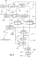
- FIG. 9 is a schematic block diagram of one example of a device for generating the optimum reconstruction level y K and the optimum decision threshold x K .
- a clock 88 generates a clock signal that is applied to a counter 90 that accumulates the clock pulses generated by clock 88.
- the counter signal 92 which constitutes the accumulated clock pulse signal, is applied to memory 94 that stores the histogram P x (x).
- This memory may correspond to the memory 72 of Figure 7 in which the histogram is generated and stored.
- the counter output 92 therefore generates a sequential set of addresses that are applied to memory 94 to generate an output 96 that includes the values of the histogram P x (x) stored at each one of the sequential addresses of memory 94.
- the sequential set of addresses generated by the counter 90 are also applied to a latch 98 that stores each sequential address for one clock signal.
- Latch 98 is reset by reset signal 100 that is generated by a delay 102 that delays the clock signal 104 by one clock cycle.
- Each sequential address signal corresponds to x in equation (1) which is applied to multiplier 106.
- the value that is stored in memory 94 at each address location is also applied to multiplier 106 so that the value of P x (x) at a particular address location x is multiplied by x to produce a series of first results 108.
- the series of first results 108 are accumulated in accumulator 110 and applied to divider 112.
- the output 96 of memory 94 which corresponds to the value of the histogram at each one of the sequential address locations for x, is accumulated in accumulator 114.
- This accumulated value is also applied to divider 112 which divides the accumulated value from accumulator 110 by the accumulated value for accumulator 114.
- the accumulated value for accumulator 110 corresponds to the integrated value of the numerator of equation (1).
- the accumulated value of accumulator 114 corresponds to the integrated value of the denominator of equation (1).
- the output 116 of divider 112 therefore corresponds to the optimum reconstruction level y K .
- a comparator 118 compares the sequential address signal 92 with the value of x K-1 .
- an enable signal 120 is generated that resets accumulator 110, accumulator 114, and counter 90.
- Enable signal 120 is also used to enable divider 112 to generate the output 116 which corresponds to the optimum reconstruction level y K .
- the output 116 is applied to delay device 220 which delays the output 116 by the period of the enable signal 120.
- the output of the delay 220 is applied to latch 122 which latches the output from delay 220 and applies the delayed output to adder 124.
- Adder 124 adds the output y K with a delayed output of the previous division that corresponds to y K-1 .
- the output of the adder 124 is then applied to a divide by two circuit 126 to produce an output 128 that corresponds to the optimum decision threshold x K .
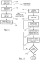
- Figure 10 is a flow chart 130 for determining y K .
- the histogram P x (x) is generated. This step is disclosed in more detail in Figure 12.
- y K is set at zero.
- addresses are generated for x from x K to x K-1 .
- each of these addresses is used to read the value of the histogram P x (x) for address values of x between x K and x K-1 .
- each value of x is multiplied by each corresponding value of P x (x).
- each of the results of the multiplications are accumulated to obtain result number 1.
- each of the values of P x (x) that were read at step 138 are accumulated to obtain result number 2.
- y K is calculated by dividing result number 1 by result number 2.
- the value of K is incremented by 1.
- decision black 150 the value of K is compared with the value of L. If the value of K is greater than L the process is done. If the value of K is less than or equal to L the process is continued at step 134.
- Figure 11 is a flow chart 152 for determining x K .
- the value of y K-1 is determined.
- the value of y K is determined.
- the value of y K and the value of y K-1 are added together.
- the values of y K and y K-1 divided to produce x K are added together.
- step 172 the value stored at address x(nT) is incremented by a value of one.
- decision block 176 it is determined whether the time set on the timer has expired. If it has, the process is done. If the time on the timer has not expired, the process is continued at step 168.
Landscapes
- Engineering & Computer Science (AREA)
- Power Engineering (AREA)
- Computer Networks & Wireless Communication (AREA)
- Signal Processing (AREA)
- Analogue/Digital Conversion (AREA)
- Compression, Expansion, Code Conversion, And Decoders (AREA)
- Digital Transmission Methods That Use Modulated Carrier Waves (AREA)
Applications Claiming Priority (4)
| Application Number | Priority Date | Filing Date | Title |
|---|---|---|---|
| US7006597P | 1997-12-30 | 1997-12-30 | |
| US70065P | 1997-12-30 | ||
| US61510 | 1998-04-16 | ||
| US09/061,510 US6292126B1 (en) | 1997-12-30 | 1998-04-16 | Quantizer that uses optimum decision thresholds |
Publications (2)
| Publication Number | Publication Date |
|---|---|
| EP0959597A2 true EP0959597A2 (de) | 1999-11-24 |
| EP0959597A3 EP0959597A3 (de) | 2000-05-17 |
Family
ID=26741148
Family Applications (1)
| Application Number | Title | Priority Date | Filing Date |
|---|---|---|---|
| EP98460065A Withdrawn EP0959597A3 (de) | 1997-12-30 | 1998-12-30 | Quantisierer, der die optimalen Entscheidungspegel verwendet |
Country Status (4)
| Country | Link |
|---|---|
| US (1) | US6292126B1 (de) |
| EP (1) | EP0959597A3 (de) |
| JP (1) | JPH11251904A (de) |
| CA (1) | CA2256067A1 (de) |
Cited By (2)
| Publication number | Priority date | Publication date | Assignee | Title |
|---|---|---|---|---|
| EP1453238A1 (de) * | 2003-02-25 | 2004-09-01 | CoreOptics, Inc., c/o The Corporation Trust Center | Verfahren und Schaltung zur Einstellung der Abtastphase in einem überabgetasteten Empfänger |
| WO2024256029A1 (en) * | 2023-06-16 | 2024-12-19 | Huawei Technologies Co., Ltd. | Pattern dependent thresholds for slicing a multi-level signal |
Families Citing this family (12)
| Publication number | Priority date | Publication date | Assignee | Title |
|---|---|---|---|---|
| KR100404180B1 (ko) * | 1999-07-06 | 2003-11-03 | 엘지전자 주식회사 | 통신시스템에서의 기지국 신호 복조 장치 |
| KR100364753B1 (ko) * | 1999-11-19 | 2002-12-16 | 엘지전자 주식회사 | 칼라 히스토그램의 빈값 양자화 방법 |
| JP3588092B2 (ja) * | 2002-09-30 | 2004-11-10 | 松下電器産業株式会社 | 受信装置及びブラインド受信方法 |
| US7324611B2 (en) * | 2003-03-18 | 2008-01-29 | The Boeing Company | Symbol decision adjustment in demodulator |
| EP1676193A4 (de) * | 2003-10-24 | 2006-11-08 | Tyco Telecomm Us Inc | System und verfahren zur einstellung von soft-entscheidungs-schwellen in einem soft-entscheidungs-fehlerkorrektursystem |
| JP2006003303A (ja) * | 2004-06-21 | 2006-01-05 | Fujitsu Ten Ltd | レーダ装置 |
| EP1635529A1 (de) * | 2004-09-09 | 2006-03-15 | Daniel Akenine | Verfahren und Computerprodukt zum Belegen der Zeit und des Inhalts von Datensätzen in einem überwachten System |
| US20070199049A1 (en) * | 2005-09-28 | 2007-08-23 | Ubiquitynet, Inc. | Broadband network security and authorization method, system and architecture |
| JP2009515185A (ja) * | 2005-11-09 | 2009-04-09 | コーニンクレッカ フィリップス エレクトロニクス エヌ ヴィ | 流体を検査する装置 |
| WO2008046492A1 (en) * | 2006-10-20 | 2008-04-24 | Dolby Sweden Ab | Apparatus and method for encoding an information signal |
| JP5757446B2 (ja) * | 2011-06-09 | 2015-07-29 | ソニー株式会社 | 画像処理装置および方法 |
| JP2013029953A (ja) * | 2011-07-28 | 2013-02-07 | Sony Corp | 画像処理装置および方法 |
Family Cites Families (7)
| Publication number | Priority date | Publication date | Assignee | Title |
|---|---|---|---|---|
| US3931596A (en) * | 1974-09-30 | 1976-01-06 | Bell Telephone Laboratories, Incorporated | Adaptive quantizer apparatus using training mode |
| JPS56136093A (en) * | 1980-03-26 | 1981-10-23 | Fuji Photo Film Co Ltd | Adaptive quantizer |
| US4381428A (en) * | 1981-05-11 | 1983-04-26 | The United States Of America As Represented By The Secretary Of The Navy | Adaptive quantizer for acoustic binary information transmission |
| US4470146A (en) * | 1982-04-30 | 1984-09-04 | Communications Satellite Corporation | Adaptive quantizer with instantaneous error robustness |
| EP0320511B1 (de) | 1987-06-22 | 1993-08-18 | EASTMAN KODAK COMPANY (a New Jersey corporation) | Blockadaptive prädiktionskodierung mit adaptiver verstärkung und vorspannung |
| US5337373A (en) * | 1991-10-24 | 1994-08-09 | International Business Machines Corporation | Automatic threshold generation technique |
| US5295155A (en) | 1992-10-30 | 1994-03-15 | International Business Machines Corporation | Multi-level digital data regeneration system |
-
1998
- 1998-04-16 US US09/061,510 patent/US6292126B1/en not_active Expired - Lifetime
- 1998-12-24 JP JP10366778A patent/JPH11251904A/ja active Pending
- 1998-12-29 CA CA002256067A patent/CA2256067A1/en not_active Abandoned
- 1998-12-30 EP EP98460065A patent/EP0959597A3/de not_active Withdrawn
Cited By (5)
| Publication number | Priority date | Publication date | Assignee | Title |
|---|---|---|---|---|
| EP1453238A1 (de) * | 2003-02-25 | 2004-09-01 | CoreOptics, Inc., c/o The Corporation Trust Center | Verfahren und Schaltung zur Einstellung der Abtastphase in einem überabgetasteten Empfänger |
| WO2004077737A1 (en) * | 2003-02-25 | 2004-09-10 | Coreoptics Inc. | Self-timing method for adjustment of a sampling phase in an oversampling receiver and circuit |
| JP2006520553A (ja) * | 2003-02-25 | 2006-09-07 | コアオプティックス・インコーポレイテッド | オーバーサンプリングレシーバにおけるサンプリング位相調整のためのセルフタイミング法および回路 |
| US8068572B2 (en) | 2003-02-25 | 2011-11-29 | Cisco Technology, Inc. | Self-timing method for adjustment of a sampling phase in an oversampling receiver and circuit |
| WO2024256029A1 (en) * | 2023-06-16 | 2024-12-19 | Huawei Technologies Co., Ltd. | Pattern dependent thresholds for slicing a multi-level signal |
Also Published As
| Publication number | Publication date |
|---|---|
| EP0959597A3 (de) | 2000-05-17 |
| US6292126B1 (en) | 2001-09-18 |
| JPH11251904A (ja) | 1999-09-17 |
| CA2256067A1 (en) | 1999-06-30 |
Similar Documents
| Publication | Publication Date | Title |
|---|---|---|
| US6292126B1 (en) | Quantizer that uses optimum decision thresholds | |
| US6510188B1 (en) | All digital automatic gain control circuit | |
| EP0769364B1 (de) | Phasenabgleich, insbesondere für HDTV-Empfänger | |
| US6175599B1 (en) | Method and apparatus for transmitting and receiving digital data over a bandpass channel | |
| US5459762A (en) | Variable multi-threshold detection for 0.3-GMSK | |
| US4309772A (en) | Soft quantizer for FM radio binary digital signaling | |
| EP0034383B1 (de) | Kohärenter Empfänger für winkelmodulierte Datensignale | |
| US5214670A (en) | Equalization system and method for equalizing a base-band telecommunication line | |
| KR100544218B1 (ko) | 디지털 데이터 전송 장치, 전송로 부호화 방법, 및 복호방법 | |
| WO2012021299A1 (en) | Digital two way automatic communication system (twacs) outbound receiver and method | |
| EP0572376B1 (de) | Spektral wirksames digital-fm-modulationssystem | |
| KR19980033375A (ko) | 직교 주파수 분할 다중화 방식을 사용하는 수신기에서의 타이밍동기화 | |
| US6317062B1 (en) | Method and apparatus for dynamically generating multiple level decision thresholds of an M-ary coded signal | |
| US6477215B1 (en) | Sampling control loop for a receiver for digitally transmitted signals | |
| US6363111B1 (en) | Control loop for adaptive multilevel detection of a data signal | |
| US4563681A (en) | Tone receiver for digital data communication systems | |
| EP0580482A1 (de) | Digitaler Empfangsfilter | |
| Azizzadeh et al. | Degradation of BER by group delay in digital phase modulation | |
| EP1139619A1 (de) | Kanalschätzung mittels einer wahrscheinlichkeitumsetzungstabelle | |
| AU9701198A (en) | Quantizer that uses optimum decision thresholds | |
| US6463106B1 (en) | Receiver with adaptive processing | |
| US6026131A (en) | Automatic gain control systems | |
| NL8700075A (nl) | Datatransmissiestelsel voorzien van versmeringsfilters. | |
| US4780886A (en) | Device for detecting a data signal energy drop | |
| RU2039416C1 (ru) | Цифровой адаптивный приемник дискретных сигналов |
Legal Events
| Date | Code | Title | Description |
|---|---|---|---|
| PUAI | Public reference made under article 153(3) epc to a published international application that has entered the european phase |
Free format text: ORIGINAL CODE: 0009012 |
|
| AK | Designated contracting states |
Kind code of ref document: A2 Designated state(s): AT BE CH CY DE DK ES FI FR GB GR IE IT LI LU MC NL PT SE |
|
| AX | Request for extension of the european patent |
Free format text: AL;LT;LV;MK;RO;SI |
|
| PUAL | Search report despatched |
Free format text: ORIGINAL CODE: 0009013 |
|
| AK | Designated contracting states |
Kind code of ref document: A3 Designated state(s): AT BE CH CY DE DK ES FI FR GB GR IE IT LI LU MC NL PT SE |
|
| AX | Request for extension of the european patent |
Free format text: AL;LT;LV;MK;RO;SI |
|
| RIC1 | Information provided on ipc code assigned before grant |
Free format text: 7H 04L 25/06 A, 7H 03M 1/08 B, 7H 03M 1/12 B |
|
| 17P | Request for examination filed |
Effective date: 20001115 |
|
| AKX | Designation fees paid |
Free format text: AT BE CH CY DE DK ES FI FR GB GR IE IT LI LU MC NL PT SE |
|
| STAA | Information on the status of an ep patent application or granted ep patent |
Free format text: STATUS: THE APPLICATION IS DEEMED TO BE WITHDRAWN |
|
| 18D | Application deemed to be withdrawn |
Effective date: 20030701 |