EP0961207B1 - Gerät zur Kommunikation zwischen einem Neuronalen Netzwerk und einem Benutzersystem über einen Bus - Google Patents
Gerät zur Kommunikation zwischen einem Neuronalen Netzwerk und einem Benutzersystem über einen Bus Download PDFInfo
- Publication number
- EP0961207B1 EP0961207B1 EP99401228A EP99401228A EP0961207B1 EP 0961207 B1 EP0961207 B1 EP 0961207B1 EP 99401228 A EP99401228 A EP 99401228A EP 99401228 A EP99401228 A EP 99401228A EP 0961207 B1 EP0961207 B1 EP 0961207B1
- Authority
- EP
- European Patent Office
- Prior art keywords
- converter
- output
- converters
- intermediate node
- control circuit
- Prior art date
- Legal status (The legal status is an assumption and is not a legal conclusion. Google has not performed a legal analysis and makes no representation as to the accuracy of the status listed.)
- Expired - Lifetime
Links
Images




Classifications
-
- G—PHYSICS
- G06—COMPUTING OR CALCULATING; COUNTING
- G06N—COMPUTING ARRANGEMENTS BASED ON SPECIFIC COMPUTATIONAL MODELS
- G06N3/00—Computing arrangements based on biological models
- G06N3/02—Neural networks
- G06N3/04—Architecture, e.g. interconnection topology
- G06N3/049—Temporal neural networks, e.g. delay elements, oscillating neurons or pulsed inputs
-
- G—PHYSICS
- G06—COMPUTING OR CALCULATING; COUNTING
- G06N—COMPUTING ARRANGEMENTS BASED ON SPECIFIC COMPUTATIONAL MODELS
- G06N3/00—Computing arrangements based on biological models
- G06N3/02—Neural networks
- G06N3/06—Physical realisation, i.e. hardware implementation of neural networks, neurons or parts of neurons
- G06N3/063—Physical realisation, i.e. hardware implementation of neural networks, neurons or parts of neurons using electronic means
Definitions
- the present invention relates to a device for communication between a neural network of a system perceptual and a user system through a communication bus which must pass through information in the form of asynchronous pulses generated from analog signals produced by neurons in the network.
- the artificial neurons of a network 1 are associated with current / frequency converters 2 which account for neuron activity.
- 3a is symbolized the activity of a neuron which, for example, can be represented by an analog variable (current or voltage) variable at over time.
- This activity is converted by converter 2, into a series of pulses 3b whose frequency is proportional to the amplitude of the quantity analog.
- the outputs of converters 2 are applied, via the encoder 4, to the communication bus 5 according to a code specific to each neuron.
- Figure 2 shows the activity of three neurons coded on the five wires from bus 5, namely: on the first and fourth wires for the first neuron (code 10010), on the second and third son for the second (code 01100) and on the fourth and fifth sons for the third (code 00011).
- Communication bus 5 leads to a circuit of use 6 more or less distant from network 1.
- This circuit includes a decoder 7 and accumulators of activity 8, each accumulator restoring the signal activity of the neuron with which it is associated, as is illustrated in 3c.
- Such an arbitration system can be that described in an article by J. Lazzaro et al. titled “Silicon auditory processors as computer peripherals ", published in the journal IEEE Transaction on Neural Networks, vol. 4 pages 523 to 528, May 1993.
- a neuron wishes to send a impulse it makes a request to the arbitration system who checks if the communication bus is free and who returns a transmit authorization signal to the neuron. Yes so two neurons want to access the bus at the same time, the arbitration system, thanks to an arbitration tree, chooses one of the two neurons and makes the other wait. But if collisions can be avoided, it comes at a price of a remarkable complexity of the circuits. Indeed, it is necessary provide request and authorization drivers for each row and each column of the network, as well as a tree arbitration for rows and columns, which it results in an increased complexity of the circuit. In addition, the transmission speed is considerably scaled down.
- the object of the invention is to provide a device for communication between a neural network and a system user via a transmission bus information that does not complicate the organs mounted in upstream and downstream of the bus and which allows through arbitration improved to ensure transmission speed higher in quality equal to that obtainable, with a system operating without arbitration.
- the invention therefore relates to a device for communication presenting the characteristics of the claim 1.
- the invention exploits for the implementation of arbitration, the presence of a pulse on the converter output corresponding to the neuron active at the time considered to block the operation of all other converters and this that the pulse produced by this neuron lasts.
- the result a very simple assembly which requires only a minimum of simple components, arbitration remaining otherwise perfectly reliable.
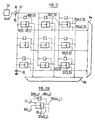
- Figure 3 represents a simplified diagram of a following communication device the invention.
- This scheme which is similar in principle to that of figure 1, corresponds by way of example to a matrix of 3 X 3 neurons.
- a matrix of 3 X 3 neurons can have a very large number of neurons, all connected in the same way, any neuron with coordinates i, j in the matrix being connected according to the detail diagram of the Figure 3A.
- a converter is associated current / frequency 2 (i, j), whose output signal is transmitted both to a line encoder 4a and to a line encoder column 4b, via connections 35a (i, j) and 35b (i, j), respectively.
- Each encoder is connected to a bus communication (not shown). According to the invention, means are provided to arbitrate access to buses communication by converters 2.
- These arbitration means firstly comprise blocking means connected in common to all the converters 2 (i, j) to transmit to them a temporary blocking command.
- These blocking means comprise a voltage source 14 delivering a direct voltage V ref .
- This voltage source is connected to a voltage divider comprising a resistor 15, itself connected to a capacitor 16 which is also connected to ground.
- This capacity 16 can be the parasitic capacity of the node 17 with respect to the mass.
- This node 17 is connected in common to the outputs 20 (i, j) of inhibition control circuits 18 (i, j) associated respectively with each of the voltage / frequency converters 2 (i, j).
- Each inhibition control circuit 18 (i, j) is further connected to the output of its associated converter for that it can detect the presence of an impulse. Through elsewhere the intermediate node 17 is connected to terminals respective blocking 19 (i, j) of converters 2 (i, j).
- the control circuit inhibition 18 when due to the activity of a neuron given 1 (i, j), an impulse appears at the output of the associated converter, the control circuit inhibition 18 (i, j) will activate the blocking means. it amounts to modifying the potential of node 17 which will then take such a value on the blocking terminals 19 (i, j) of voltage / frequency converters that the operation of these is suspended, however the operation of the converter corresponding to the neuron active remains maintained.
- Figures 4 to 6 show a diagram of principle three different embodiments of the circuit inhibition command.
- elements equivalents have been identified by identical references followed by the letters A, B and C. respectively elsewhere, we have taken up some other elements already shown in Figures 3 and 3A.
- these figures show only one converter while of course all the converters are associated with their own muting control circuit arranged as shown respectively in FIGS. 4 to 6.
- the output of the voltage / frequency converter 2A is connected to the gate of a transistor 21 of the inhibition control circuit 18A, the source-drain path of this transistor being connected between a current source 22 and the intermediate node 17. Consequently, when the transistor 21 is made conductive by a pulse produced by the converter 2A (a corresponding neuron of the matrix network is active), a current I H is injected into the node 17 which modifies the potential on the blocking terminals 19A of all converters. This variation in potential is capable of blocking the converters even if their associated neurons are active at the instant considered, with the exception of the one whose corresponding neuron is active.
- control circuit inhibition 18B includes a transistor 23 whose gate is connected to the output of converter 2B and whose path source-drain is connected between ground and node 17. In this case, the inhibition control circuit 18B allows therefore to bring the bounds of blocking of all converters, operation of the converter whose neuron is active at the moment considered, not being influenced by the state of its terminal blocking.
- control circuit inhibition 18C includes a capacity 24 connected between the output of converter 2C and node 17, the latter being further connected to the output of the voltage source 14 by via a diode 25.
- the node 17 follows the charging voltage of capacitor 24.
- FIG. 7 represents an exemplary embodiment of a current / frequency converter and its circuit associated inhibition command which can more particularly be used in the variant of figure 4 to fill the function of block 2A in association with the inhibition command in the version of FIG. 4.
- This converter comprises a Schmitt flip-flop 26 whose input 27 receives a voltage V in from a neuron in the network. This input is connected to ground via a capacitance 28 which can be the parasitic capacitance of the input 27 with respect to ground.
- the Schmitt rocker switches between two voltages called VHP and VHM hysteresis.
- the voltage VHM is fixed and comes from a reference source 29. It is applied to the gate of a transistor 30.
- the other hysteresis voltage VHP of the flip-flop is applied to the blocking terminal 19 of the converter which is in fact the gate of a transistor 31.
- the output of the Schmitt seesaw 26 is connected to a set of two inverters 32 and 33 mounted one after the other.
- the output of the second inverter 33 is connected to the transistor 21 of the inhibition control circuit 18A.
- the output of the inverter 33 is also connected to the gate of a transistor 34 whose source-drain path is connected between ground and an output 35 of converter 2A.
- FIG. 7 also shows in a) a form of the input voltage V IN of the Schmitt flip-flop 26 and in b) the voltage V OUT supplied to the output 35.
- the emission of a pulse at the output 35 also causes the conduction of the transistor 21 of the inhibition control circuit 18A so that the current source 22 can now charge the node 17 where the VHP voltage prevails.
- This increases this voltage and thus the value of the hysteresis voltage of the other converters connected to the other neurons. Consequently, in order to be able to switch, the Schmitt flip-flops of these other converters must receive an input voltage of a value now greater than the initial VHP voltage which was equal to VHP ref (the voltage V ref in FIG. 3).
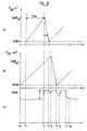
- Figure 8 graphically illustrates what has just been described. It represents in a) the voltage on the input of a any converter 2 (i, j) of figure 3A, this converter now designated by 2A-N1 and that we suppose, for example, to be associated with a neuron called N1.
- Figure 8 shows in b) the input voltage of a other converters (designated by 2A-N2) of which will call the associated neuron N2.
- neurons N1 and N2 are successively active and that the activity of neuron N1 is more intense but later than that of neuron N2.
- this time diagram is not at constant scale, this to facilitate the highlighting the evolution of tensions as a function of time. So by example, the interval between times t1 and t2 can last 1 ms while the time interval between t2 and t3 can only last 50 ns. In general, the rise of the input voltage of a converter is much longer that its descent, this roughly in the proportions that we just indicated.
- Figure 8 shows in c) the evolution of the VHP voltage on node 17 in case the activities of neurons N1 and N2 as defined above coincide partially in time.
- the pulses generated by the converters 2A-N1 and 2A-N2 would overlap at least in part and it so what would have been called above a "collision" which would make it impossible to transmit on the bus 5 the impulses due to the almost simultaneous activity of the two neurons.
- the voltage VHP is maintained at the upper level for the duration of the output pulse of the converter 2A-N2 after which its level decreases again from time t5. It is also assumed that from this moment another neuron is active until time t7 after which the neurons of the network no longer manifest, for a time at least, an activity. As a result, the voltage VHP returns to the reference value VHP ref , no inhibition block being active from time t8.
- Figure 9 shows in a) the shape of the tension input of a converter fitted with a control circuit 18C inhibition designed according to FIG. 6.
- the tension of node 17 has the form shown in b) in FIG. 9, in the event of activity on the neuron considered.
- the timescale is not respected.
- Figure 10 shows the pulses produced at the same time by five neurons on the one hand in a system (in a) devoid of the provisions according to the invention and a system (in b) in which the converters are provided with means arbitration according to one or other of the variants that we just described.
- the impulses appear one after the other by being well separated in time.
Landscapes
- Engineering & Computer Science (AREA)
- Physics & Mathematics (AREA)
- Theoretical Computer Science (AREA)
- Health & Medical Sciences (AREA)
- Life Sciences & Earth Sciences (AREA)
- Biomedical Technology (AREA)
- Biophysics (AREA)
- General Health & Medical Sciences (AREA)
- General Physics & Mathematics (AREA)
- Evolutionary Computation (AREA)
- Computational Linguistics (AREA)
- Molecular Biology (AREA)
- Computing Systems (AREA)
- General Engineering & Computer Science (AREA)
- Data Mining & Analysis (AREA)
- Mathematical Physics (AREA)
- Software Systems (AREA)
- Artificial Intelligence (AREA)
- Neurology (AREA)
- Small-Scale Networks (AREA)
- Arrangements For Transmission Of Measured Signals (AREA)
Claims (7)
- Kommunikationsvorrichtung zwischen einem aus in einer adressierbaren Matrix verbundenen Neuronen zusammengesetzten Neuronennetz (1) und einem Nutzungssystem (6) durch einen Übertragungsbus (5), wobei diese Vorrichtung einen Aktivitäts- / Frequenzumwandler je Neuron (2 (i, j)) umfasst, der dazu bestimmt ist, auf seinem Ausgang Impulse zu liefern, deren Frequenz die Aktivität dieses Neurons darstellt, wobei die Ausgänge der den Neuronen der Matrix zugeordneten Umwandler an einen Codierer (4) angeschlossen sind, durch den die besagten Impulse einem dem Neuron zugehörigen binären Code zugeordnet werden, der ihre Produktion hervorgerufen hat, und wobei der besagte Codierer (4) für die Übertragung der auf diese Weise hergestellten Codes zum Nutzungssystem (6) an den besagten Bus (5) angeschlossen ist, wobei die besagte Vorrichtung ebenfalls Schlichtungsmittel zur Bestimmung der Reihenfolge der verschiedenen von den Neuronen der besagten Kette produzierten Codes auf dem Übertragungsbus (5) umfasst,
dadurch gekennzeichnet, dass
die besagten Schlichtungsmittel für jeden der besagten Umwandler einen Steuerschaltkreis (18 (i, j)) zur Verhinderung der Funktion seines zugeordneten Umwandlers sowie Blockiermittel (14, 15, 16, 17) umfasst, die gemeinsam an alle Umwandler angeschlossen sind, um ihnen einen temporären Blockierbefehl zu übertragen, wobei jeder Schaltkreis zur Verhinderung angeordnet ist, um das Vorhandensein eines Impulses am Ausgang seines zugeordneten Umwandlers festzustellen und um während des Vorhandenseins eines derartigen Impulses die besagten Blockiermittel zu aktivieren, damit sie den besagten temporären Blockierbefehl ihrer Funktion an die anderen Umwandler übertragen. - Kommunikationsvorrichtung gemäß Anspruch 1, dadurch gekennzeichnet, dass die besagten Blockiermittel eine Referenzspannungsquelle (14) umfassen, die an einen Spannungsteiler (15, 16) angeschlossen ist, der einen zwischengeschalteten Knotenpunkt (17) aufweist, der einerseits an jeden der besagten Steuerschaltkreise angeschlossen ist und andererseits an einen Blockiereingang (19, (i, j)) jeder der besagten Umwandler, dass jeder Steuerschaltkreis angeordnet ist, um das Potenzial des besagten zwischengeschalteten Knotenpunktes (17) zu ändern, während ein Impuls am Ausgang des ihm zugeordneten Umwandlers vorhanden ist, wobei die Änderung des Potenzials bei Aktivierung der besagten Blockiereingänge aller anderen Umwandler die Produktion eines Impulses durch diese verhindert.
- Kommunikationsvorrichtung gemäß Anspruch 2, dadurch gekennzeichnet, dass der besagte Spannungsteiler die Reihenschaltung aus einem Widerstand (15) und einer Kapazität (16) umfasst, deren gemeinsamer Punkt den besagten zwischengeschalteten Knotenpunkt (17) bildet, wobei die Reihenschaltung zwischen der besagten Referenzspannungsquelle (14) und der Masse angeschlossen ist.
- Kommunikationsvorrichtung gemäß Anspruch 3, in der jeder Umwandler einen Schmitt-Trigger (26) umfasst, dessen Eingang (27) mit dem aus dem an diesen Umwandler angeschlossenen Neuron stammenden Aktivitätssignal (VIN) beaufschlagt wird und dessen Ausgang (36) an den besagten Codierer (4) angeschlossen ist, wobei dieser Trigger (26) an zwei Hysteresespannungsquellen (VHP, VHM) angeschlossen ist, zwischen denen sich das besagte Aktivitätssignal (VIN) entwickeln muss, um den Trigger (26) zu kippen und somit die Länge und den Abstand der besagten Impulse zu bestimmen, wobei diese Vorrichtung dadurch gekennzeichnet ist, dass eine der zwei Hysteresespannungsquellen (VHM, VHP) der zwischengeschaltete Knoten (17) des besagten Spannungsteilers ist.
- Kommunikationsvorrichtung gemäß Anspruch 4, dadurch gekennzeichnet, dass jede Steuerschaltung zur Verhinderung (18A) einen Transistor (21) umfasst, dessen Gitter an den besagten Ausgang (36A) des zugeordneten Umwandlers (2A) angeschlossen ist und dessen Laufbahn Quelle - Drain zwischen einer Stromquelle (22) und dem besagten zwischengeschalteten Knotenpunkt (17) verbunden ist.
- Kommunikationsvorrichtung gemäß Anspruch 4, dadurch gekennzeichnet, dass jeder Steuerschaltkreis zur Verhinderung (18B) einen Transistor (21) umfasst, dessen Gitter an den besagten Ausgang (36B) des zugeordneten Umwandlers (2B) angeschlossen ist, und dessen Laufbahn Quelle - Drain zwischen dem besagten zwischengeschalteten Knotenpunkt (17) des besagten Teilers und der Masse verbunden ist.
- Kommunikationsvorrichtung gemäß Anspruch 4, dadurch gekennzeichnet, dass jeder Steuerschaltkreis zur Verhinderung (18C) eine Kapazität (24) umfasst, die zwischen dem besagten Ausgang (36C) des Umwandlers und dem besagten zwischengeschalteten Knotenpunkt (17) angebracht ist, und eine Diode (25), die zwischen der besagten Referenzspannungsquelle und dem besagten zwischengeschalteten Knotenpunkt (17) des Teilers angeschlossen ist.
Applications Claiming Priority (2)
| Application Number | Priority Date | Filing Date | Title |
|---|---|---|---|
| FR9806535A FR2778994B1 (fr) | 1998-05-25 | 1998-05-25 | Dispositif de communication entre un reseau neuronal et un systeme utilisateur par l'intermediaire d'un bus |
| FR9806535 | 1998-05-25 |
Publications (2)
| Publication Number | Publication Date |
|---|---|
| EP0961207A1 EP0961207A1 (de) | 1999-12-01 |
| EP0961207B1 true EP0961207B1 (de) | 2002-07-31 |
Family
ID=9526657
Family Applications (1)
| Application Number | Title | Priority Date | Filing Date |
|---|---|---|---|
| EP99401228A Expired - Lifetime EP0961207B1 (de) | 1998-05-25 | 1999-05-21 | Gerät zur Kommunikation zwischen einem Neuronalen Netzwerk und einem Benutzersystem über einen Bus |
Country Status (4)
| Country | Link |
|---|---|
| US (1) | US6567485B1 (de) |
| EP (1) | EP0961207B1 (de) |
| DE (1) | DE69902315T2 (de) |
| FR (1) | FR2778994B1 (de) |
Families Citing this family (3)
| Publication number | Priority date | Publication date | Assignee | Title |
|---|---|---|---|---|
| CH694232A5 (fr) * | 2000-04-27 | 2004-09-30 | Suisse Electronique Microtech | Procédé d'encodage temporel d'une pluralité d'informations pouvant être représentées par des vecteurs. |
| FR2846490B1 (fr) * | 2002-10-24 | 2005-01-14 | Suisse Electronique Microtech | Systeme d'analyse spatiale d'une grandeur physique |
| CA2486949A1 (fr) | 2004-12-09 | 2006-06-09 | Christian Cloutier | Systeme et methode pour la detection des chutes et du suivi des niveaux d'activite a distance chez des personnes en perte d'autonomie |
Family Cites Families (5)
| Publication number | Priority date | Publication date | Assignee | Title |
|---|---|---|---|---|
| US4652873A (en) * | 1984-01-18 | 1987-03-24 | The Babcock & Wilcox Company | Access control for a plurality of modules to a common bus |
| JPH0646733B2 (ja) * | 1987-06-30 | 1994-06-15 | 沖電気工業株式会社 | 1つの伝送媒体を共有する競合制御方式 |
| US4755990A (en) * | 1987-10-08 | 1988-07-05 | Karl Suss America, Inc. | Collision avoidance in a multinode data communication network |
| US5175731A (en) * | 1990-12-11 | 1992-12-29 | International Business Machines Corporation | Arbitration circuit for a multimedia system |
| EP0562222B1 (de) * | 1992-03-27 | 1999-05-12 | Alcatel | Anordnung zur Zugriffssteuerung |
-
1998
- 1998-05-25 FR FR9806535A patent/FR2778994B1/fr not_active Expired - Fee Related
-
1999
- 1999-05-21 DE DE69902315T patent/DE69902315T2/de not_active Expired - Fee Related
- 1999-05-21 EP EP99401228A patent/EP0961207B1/de not_active Expired - Lifetime
- 1999-05-25 US US09/318,663 patent/US6567485B1/en not_active Expired - Fee Related
Also Published As
| Publication number | Publication date |
|---|---|
| FR2778994B1 (fr) | 2001-08-31 |
| DE69902315T2 (de) | 2003-03-13 |
| EP0961207A1 (de) | 1999-12-01 |
| FR2778994A1 (fr) | 1999-11-26 |
| US6567485B1 (en) | 2003-05-20 |
| DE69902315D1 (de) | 2002-09-05 |
Similar Documents
| Publication | Publication Date | Title |
|---|---|---|
| CH692164A5 (fr) | Cellule photoélectrique à amplification stabilisée. | |
| EP0631240A1 (de) | Schaltungsanordnung zur Datenübertragung | |
| WO1990007185A1 (fr) | Dispositif de traitement de donnees comportant une memoire non volatile electriquement effaçable et reprogrammable | |
| FR2682203A1 (fr) | Systeme de transmission de donnees. | |
| FR2623674A1 (fr) | Dispositif de transmission d'informations pour vehicule automobile et procede de mise en oeuvre d'un tel dispositif | |
| EP1107259A1 (de) | Leseschaltung für integrierte Speicherschaltung | |
| EP3248305B1 (de) | Ethernet-switch für faseroptisches netzwerk | |
| EP0961207B1 (de) | Gerät zur Kommunikation zwischen einem Neuronalen Netzwerk und einem Benutzersystem über einen Bus | |
| FR2754957A1 (fr) | Procede de decodage d'un signal numerique ainsi qu'un systeme de bus et une unite peripherique pour sa mise en oeuvre | |
| EP0464778B1 (de) | Frankiermaschine mit einer als Schnittstelle dienenden gedruckten Schaltung | |
| EP0092284B1 (de) | Verfahren und System zur Datenübertragung über eine Energieversorgungsleitung | |
| EP0221786B1 (de) | Anzeigetafel mit Leuchtdioden | |
| FR2792474A1 (fr) | Circuit de sortie de signal numerique | |
| CH660808A5 (fr) | Detecteur de feu de type analogique. | |
| FR2645373A1 (fr) | Procede et dispositif de reduction du bruit sur un signal codable a plusieurs niveaux predetermines | |
| FR2537368A1 (fr) | Systeme d'identification de stations locales par un poste central d'interrogation | |
| WO2020127126A1 (fr) | Procédé de configuration d'un dispositif d'éclairage de l'intérieur de l'habitacle d'un véhicule automobile | |
| FR3090524A1 (fr) | Dispositif d'éclairage de l’intérieur de l’habitacle d’un véhicule automobile comprenant une source lumineuse pourvue d’un contrôleur intégré | |
| FR2671207A1 (fr) | Reseau neuronal a operateurs binaires et procedes pour sa realisation. | |
| EP0849659B1 (de) | Digitale Rücksetzvorrichtung eines integrierten Schaltkreises | |
| EP0549992B1 (de) | Datenringnetz und Verfahren zur Übertragung von Daten über das Netz | |
| EP0848547B1 (de) | Schnittstellenschaltung für Videokamera | |
| EP0404630B1 (de) | Vorrichtung zum Empfang von über zwei kapazitiv gekoppelte Leitungen durchgehenden Informationen, insbesondere für Kraftfahrzeuge | |
| FR2670633A1 (fr) | Procede et circuit de declenchement a seuil. | |
| FR3066667B1 (fr) | " procede et systeme de transmission serie de donnees " |
Legal Events
| Date | Code | Title | Description |
|---|---|---|---|
| PUAI | Public reference made under article 153(3) epc to a published international application that has entered the european phase |
Free format text: ORIGINAL CODE: 0009012 |
|
| AK | Designated contracting states |
Kind code of ref document: A1 Designated state(s): CH DE FR GB LI |
|
| AX | Request for extension of the european patent |
Free format text: AL;LT;LV;MK;RO;SI |
|
| 17P | Request for examination filed |
Effective date: 20000320 |
|
| AKX | Designation fees paid |
Free format text: CH DE FR GB LI |
|
| GRAG | Despatch of communication of intention to grant |
Free format text: ORIGINAL CODE: EPIDOS AGRA |
|
| 17Q | First examination report despatched |
Effective date: 20011009 |
|
| GRAG | Despatch of communication of intention to grant |
Free format text: ORIGINAL CODE: EPIDOS AGRA |
|
| GRAG | Despatch of communication of intention to grant |
Free format text: ORIGINAL CODE: EPIDOS AGRA |
|
| GRAH | Despatch of communication of intention to grant a patent |
Free format text: ORIGINAL CODE: EPIDOS IGRA |
|
| GRAH | Despatch of communication of intention to grant a patent |
Free format text: ORIGINAL CODE: EPIDOS IGRA |
|
| GRAA | (expected) grant |
Free format text: ORIGINAL CODE: 0009210 |
|
| RAP1 | Party data changed (applicant data changed or rights of an application transferred) |
Owner name: CSEM CENTRE SUISSE D'ELECTRONIQUE ET DE MICROTECHN |
|
| AK | Designated contracting states |
Kind code of ref document: B1 Designated state(s): CH DE FR GB LI |
|
| REG | Reference to a national code |
Ref country code: GB Ref legal event code: FG4D Free format text: NOT ENGLISH Ref country code: CH Ref legal event code: EP |
|
| REF | Corresponds to: |
Ref document number: 69902315 Country of ref document: DE Date of ref document: 20020905 |
|
| GBT | Gb: translation of ep patent filed (gb section 77(6)(a)/1977) |
Effective date: 20021004 |
|
| PLBE | No opposition filed within time limit |
Free format text: ORIGINAL CODE: 0009261 |
|
| STAA | Information on the status of an ep patent application or granted ep patent |
Free format text: STATUS: NO OPPOSITION FILED WITHIN TIME LIMIT |
|
| 26N | No opposition filed |
Effective date: 20030506 |
|
| PGFP | Annual fee paid to national office [announced via postgrant information from national office to epo] |
Ref country code: GB Payment date: 20040514 Year of fee payment: 6 |
|
| PGFP | Annual fee paid to national office [announced via postgrant information from national office to epo] |
Ref country code: DE Payment date: 20040526 Year of fee payment: 6 |
|
| PGFP | Annual fee paid to national office [announced via postgrant information from national office to epo] |
Ref country code: FR Payment date: 20040528 Year of fee payment: 6 |
|
| PGFP | Annual fee paid to national office [announced via postgrant information from national office to epo] |
Ref country code: CH Payment date: 20040802 Year of fee payment: 6 |
|
| PG25 | Lapsed in a contracting state [announced via postgrant information from national office to epo] |
Ref country code: GB Free format text: LAPSE BECAUSE OF NON-PAYMENT OF DUE FEES Effective date: 20050521 |
|
| PG25 | Lapsed in a contracting state [announced via postgrant information from national office to epo] |
Ref country code: LI Free format text: LAPSE BECAUSE OF NON-PAYMENT OF DUE FEES Effective date: 20050531 Ref country code: CH Free format text: LAPSE BECAUSE OF NON-PAYMENT OF DUE FEES Effective date: 20050531 |
|
| PG25 | Lapsed in a contracting state [announced via postgrant information from national office to epo] |
Ref country code: DE Free format text: LAPSE BECAUSE OF NON-PAYMENT OF DUE FEES Effective date: 20051201 |
|
| REG | Reference to a national code |
Ref country code: CH Ref legal event code: PL |
|
| GBPC | Gb: european patent ceased through non-payment of renewal fee |
Effective date: 20050521 |
|
| PG25 | Lapsed in a contracting state [announced via postgrant information from national office to epo] |
Ref country code: FR Free format text: LAPSE BECAUSE OF NON-PAYMENT OF DUE FEES Effective date: 20060131 |
|
| REG | Reference to a national code |
Ref country code: FR Ref legal event code: ST Effective date: 20060131 |