EP0961344A1 - Dispositif de radiocommunication et antenne à fente en boucle - Google Patents
Dispositif de radiocommunication et antenne à fente en boucle Download PDFInfo
- Publication number
- EP0961344A1 EP0961344A1 EP99401110A EP99401110A EP0961344A1 EP 0961344 A1 EP0961344 A1 EP 0961344A1 EP 99401110 A EP99401110 A EP 99401110A EP 99401110 A EP99401110 A EP 99401110A EP 0961344 A1 EP0961344 A1 EP 0961344A1
- Authority
- EP
- European Patent Office
- Prior art keywords
- antenna
- slot
- substrate
- patch
- coupling
- Prior art date
- Legal status (The legal status is an assumption and is not a legal conclusion. Google has not performed a legal analysis and makes no representation as to the accuracy of the status listed.)
- Granted
Links
- 239000000758 substrate Substances 0.000 claims abstract description 46
- 230000008878 coupling Effects 0.000 claims abstract description 36
- 238000010168 coupling process Methods 0.000 claims abstract description 36
- 238000005859 coupling reaction Methods 0.000 claims abstract description 36
- 238000012545 processing Methods 0.000 claims description 20
- 239000004020 conductor Substances 0.000 claims description 19
- 239000000463 material Substances 0.000 claims description 6
- 230000001902 propagating effect Effects 0.000 claims description 5
- 230000005855 radiation Effects 0.000 claims description 5
- 210000000056 organ Anatomy 0.000 claims description 3
- 239000008188 pellet Substances 0.000 claims description 2
- 230000005236 sound signal Effects 0.000 claims description 2
- 238000002955 isolation Methods 0.000 claims 1
- 125000006850 spacer group Chemical group 0.000 claims 1
- 239000006260 foam Substances 0.000 abstract description 2
- 238000004519 manufacturing process Methods 0.000 abstract description 2
- 235000010603 pastilles Nutrition 0.000 description 20
- 230000003071 parasitic effect Effects 0.000 description 13
- YFXPPSKYMBTNAV-UHFFFAOYSA-N bensultap Chemical compound C=1C=CC=CC=1S(=O)(=O)SCC(N(C)C)CSS(=O)(=O)C1=CC=CC=C1 YFXPPSKYMBTNAV-UHFFFAOYSA-N 0.000 description 7
- 239000000203 mixture Substances 0.000 description 7
- 238000010586 diagram Methods 0.000 description 4
- 239000000470 constituent Substances 0.000 description 3
- 230000005684 electric field Effects 0.000 description 3
- 244000045947 parasite Species 0.000 description 3
- RYGMFSIKBFXOCR-UHFFFAOYSA-N Copper Chemical compound [Cu] RYGMFSIKBFXOCR-UHFFFAOYSA-N 0.000 description 2
- 241001644893 Entandrophragma utile Species 0.000 description 2
- 240000008042 Zea mays Species 0.000 description 2
- 230000006978 adaptation Effects 0.000 description 2
- 230000005540 biological transmission Effects 0.000 description 2
- 239000002131 composite material Substances 0.000 description 2
- 230000000694 effects Effects 0.000 description 2
- 238000000034 method Methods 0.000 description 2
- 230000000750 progressive effect Effects 0.000 description 2
- 239000007787 solid Substances 0.000 description 2
- 238000012546 transfer Methods 0.000 description 2
- 230000009466 transformation Effects 0.000 description 2
- 208000031968 Cadaver Diseases 0.000 description 1
- 241001080024 Telles Species 0.000 description 1
- 230000009286 beneficial effect Effects 0.000 description 1
- 230000008901 benefit Effects 0.000 description 1
- 230000008859 change Effects 0.000 description 1
- 238000004891 communication Methods 0.000 description 1
- 229910052802 copper Inorganic materials 0.000 description 1
- 239000010949 copper Substances 0.000 description 1
- 230000001186 cumulative effect Effects 0.000 description 1
- 238000011161 development Methods 0.000 description 1
- 238000010292 electrical insulation Methods 0.000 description 1
- 229940082150 encore Drugs 0.000 description 1
- 238000005516 engineering process Methods 0.000 description 1
- 235000021183 entrée Nutrition 0.000 description 1
- 239000003822 epoxy resin Substances 0.000 description 1
- 238000005530 etching Methods 0.000 description 1
- 238000009413 insulation Methods 0.000 description 1
- 230000003993 interaction Effects 0.000 description 1
- 238000005259 measurement Methods 0.000 description 1
- 230000004048 modification Effects 0.000 description 1
- 238000012986 modification Methods 0.000 description 1
- 230000003287 optical effect Effects 0.000 description 1
- 229920000620 organic polymer Polymers 0.000 description 1
- 229920000647 polyepoxide Polymers 0.000 description 1
- 230000035945 sensitivity Effects 0.000 description 1
Images

Classifications
-
- H—ELECTRICITY
- H01—ELECTRIC ELEMENTS
- H01Q—ANTENNAS, i.e. RADIO AERIALS
- H01Q13/00—Waveguide horns or mouths; Slot antennas; Leaky-waveguide antennas; Equivalent structures causing radiation along the transmission path of a guided wave
- H01Q13/10—Resonant slot antennas
- H01Q13/106—Microstrip slot antennas
Definitions
- the present invention relates, in general, to the devices for radiocommunication, in particular portable radiotelephones, and it relates more particularly to the antennas which can be included in such devices.
- Such an antenna is advantageously produced according to a technique planar which applies both to the realization of lines transmitting signals and that of antennas coupling between such lines and radiated waves. It is formed by etching a conductive layer deposited on the upper surface of a dielectric substrate.
- a device more specifically includes an antenna planar with a resonant slit in the form of a loop.
- Such an antenna comprises a patch consisting of a fraction of said conductive layer. Said slot separates this patch from a conductive pad constituted by a another fraction of the same conductive layer. This beach constitutes a mass of the antenna. It almost completely surrounds this patch so that the resonant slit forms an open loop around the patch.
- the antennas produced according to this technique constitute structures resonant capable of being the seat of standing electromagnetic waves. It is through these standing waves that the antenna ensures its function which is to carry out a coupling with electromagnetic waves radiated into space.
- Various forms can be taken by these waves stationary and correspond respectively to various modes of resonance of these structures.
- Each resonance mode can be described as resulting from the superposition of two waves propagating in two opposite directions on the same path and reflecting alternately at both ends of this path. This path is defined by the constituent elements of the antenna. He will be hereinafter called "resonance path". It follows the length of the slit in the form of loop in the case of the normal resonance mode of the antennas previously mentioned.
- the resonant frequency is inversely proportional for each mode at the time during which a traveling wave considered above traverses said resonance path.
- resonance modes can be established on the same path of resonance and then appear several resonance frequencies corresponding respectively to these modes.
- a mode can be defined by a number which will be called hereinafter "number of waves” and which is the number of wavelengths of a wave whose frequency is equal to the frequency of resonance corresponding to this mode, this number of wavelengths being the one contained in the length of this path. For each journey of resonance the resonance frequency is therefore proportional to this number. This number is typically close to a small integer or a fraction whose denominator is two or four.
- the expression "resonance mode” will sometimes be replaced below by the term “resonance”.
- the coupling of an antenna to a signal processing device is to say a transmitter or a receiver, is provided through a set connection which typically includes a connection line external to this antenna and connecting the latter to this member. One end of this line forms a coupling device which is included in this antenna.
- connection line is to carry a radio frequency or microwave signal from the transmitter to the antenna terminals. Throughout such a line the signal is propagates in the form of a traveling wave without undergoing, at least in principle, significant modification of its characteristics.
- the function of the coupling device is to transform the signal supplied by the connection line so that this signal excites a resonance of the antenna, that is to say that the energy of the progressive wave carrying this signal is transferred to a useful standing wave established in the antenna with characteristics defined by the latter.
- the effectiveness of a such transfer is linked to an impedance adaptation which is to be carried out between the connection line and resonant structure.
- This adaptation is generally imperfect, i.e. the coupling device reflects a part of the energy towards the connection line which gives birth in the latter to a parasitic standing wave.
- the amplitude of this wave parasite defines a standing wave rate. This rate varies depending on the frequency and the diagram of this variation defines the bandwidth (s) of the antenna.
- the antenna transfers the energy of the useful standing wave to a wave radiated in space.
- the signal supplied by the transmitter thus undergoes a first transformation to pass from the shape of a progressive wave to that of a standing wave, then a second transformation which gives it the shape of a radiated wave.
- the signal takes the same forms in the same organs but it takes them in reverse order.
- the coupling device typically has the form of a coplanar line formed in the same conductive layer than the antenna.
- This line has a conductor main connecting to the pad and surrounded by two ground conductors connecting to the antenna ground on either side of the opening of the loop.
- the present invention relates to the production of various types of apparatus.
- These devices include portable radiotelephones, radio stations, basis for these, automobiles and airplanes or air missiles.
- the antenna included in such a device can be conformed to this profile so as not to show drag annoying additional aerodynamics.
- antenna transmitting or receiving lobes are directed towards the outside of the device.
- auxiliary conductive layers have been associated with numerous known planar antennas having resonant slots in loop form. Such a layer is typically formed on the surface bottom of the antenna substrate. It then has the effect that the waves emitted by the antenna are directed in the solid angle extending above the plane of the antenna.
- a first such known antenna is described in the document of U.S. Patent 4,063,246 (Greiser). It has a shaped tablet rectangular. It has a resonant, loop-shaped slot that surrounds this pastille. This slot is the seat of a resonance mode established according to its length and corresponding to a number of waves which is approximately the number one.
- the auxiliary conductive layer of this antenna constitutes a lower ground as it is connected through the substrate to ground upper located in the plane of the patch. Coupling with waves radiated is made from the resonant slit. This slot is then said “radiative".
- the mass of the antenna extends over a significant width from the resonant slit. This type of antenna is usually designated under the name "coplanar antenna”.
- a second antenna known differs from the previous one by the use of a resonance mode different. It is described in an article: Microwave and Optical Technology Letters / vol 6, N ° 5, April 1993, page 292-294, A COMPACT SLOT LOOP ANTENNA, M. Cal, P.S. Kooi, and M.S. Leong.
- the number of waves of the resonance mode used is approximately 1/2, i.e. the perimeter of the patch extends over half a wavelength of the wave of this mode, this mode can be called "half-wave resonance".
- the radiative zone is then mainly constituted by the outer edges of the upper mass surrounding the patch and the width of this upper mass must therefore be limited.
- the choice of this width makes it possible to adjust the impedance presented by the antenna for the connection assembly.
- the lower mass layer is advantageously more extensive than the upper mass to avoid the appearance important side lobes in the spatial distribution of emission-reception.
- This type of antenna is called internationally in English "slot loop antenna" for "loop slot antenna”.
- This second known antenna has in particular a drawback which may be common to it with the first known antenna and which is that only a fraction of the power injected into the antenna is useful in certain cases, that is, only this fraction is transferred in these cases to the resonance half wave desired.
- Another fraction of this injected power can be a parasitic fraction which is transferred to parasitic resonance modes. While said half-wave resonance is established on a path constituted by the loop slot with electric field lines extending between the patch and the upper mass, these parasitic modes are the modes which are called in English "parallel plate modes" for "parallel plate modes". They are characterized in particular by electric field lines extending across the substrate enters on the one hand the upper conductive layer including the patch and the upper mass, and on the other hand the lower mass.
- the size of said parasitic power fraction depends on the various propagation speeds of the various waves giving respectively birth to the various modes of resonance. It is known that these speeds depend on the dielectric constants of the materials in which these waves spread. This is why, in order to avoid a loss of power and / or a change in frequency caused by parasitic resonances, a third and fourth known antennas differ from previous ones by the use of several materials with different dielectric constants.
- This third known antenna is described in an article: ELECTRONICS LETTERS, vol.32, n ° 18, 29th August 1996, P. 1633-1635 Forma et al. "Compact Oscillating slot loop antenna with conductor backing".
- dielectric substrate used to carry the conductive layer upper and lower mass it has another dielectric layer which covers the upper conductive layer and which has a constant higher dielectric than that of this substrate.
- This other dielectric layer is added for two purposes: one is to slow down the useful traveling waves which propagate along the loop gap a short distance above and below the antenna plan. The other aim is not to slow down the waves which propagate throughout the thickness of the substrate and which can give rise parasitic modes. The effect of the difference in speeds thus created is favor the desired half-wave resonance.
- the fourth known antenna is described in an article: IEEE TRANSACTIONS ON ANTENNAS AND PROPAGATION, Vol.43 n ° 10, October 1995, p. 1143-1148, Liu et al. "Radiation of Printed Antennas with a Coplanar Waveguide Feed ".
- the purpose of using two dielectric layers is to same as in the third known antenna except that the two layers of different dielectric constants are both interposed between the layer upper conductor and lower mass. That is, the substrate is then composite.
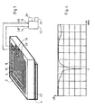
- Figure 1 shows a view of a radiocommunication device produced according to this invention, an antenna of this device being seen in perspective.
- FIG. 2 represents a top view of the antenna of the device of the figure 1.
- FIG. 3 represents a view of the same antenna in section through a vertical plane III-III of figure 2.
- FIG. 4 represents a diagram of the variation of a coefficient of reflection expressed in decibels and measured at the input of this same antenna, in function of the frequency of a signal feeding this antenna, this frequency being expressed in MHz.
- the antenna further includes a coupling device.
- this device has the form of a line of coplanar type transmission. On the one hand it has a main conductor consisting of a longitudinal coupling tape 18 extending over the surface top of the substrate. This ribbon is connected to the patch 6 in the middle of said rear edge 50.
- This device also comprises a ground conductor 20 consisting of a third and a fourth fraction of the conductive layer upper, these two fractions being located on either side of the ribbon 18. The electric field lines of the traveling waves guided by this line of transmission are established through two longitudinal slots separating this ribbon of these two fractions.
- this coupling constitutes all or part of a connection assembly which connects the resonant structure of the antenna to a said signal processing member.
- this assembly also includes a line connection which is external to the antenna.
- such an external connection line to the antenna has been symbolically represented in the form of two conducting wires 28 and 30. These two wires respectively connect the coupling tape 18 and the ground conductor 20 to a signal terminal 14 and to a ground terminal 16 of the signal processor 12. But it should be understood that such a line would in practice be preferably carried out in the form of a line coplanar, a microstrip line or a coaxial line.
- the signal processor 12 is adapted to operate at predetermined operating frequencies that are at least close to the useful resonant frequency of the antenna, i.e. which are included in a bandwidth centered on this resonant frequency. He can be composite and then have an element permanently tuned to each of these operating frequencies. It can also include a tunable element on the various operating frequencies.
- This resonant frequency F is such that the product PxF of this frequency by the said perimeter P of the patch is close to half V / 2 of a speed of mean propagation V of an electromagnetic wave having this frequency and propagating in this antenna along said resonant slot. That is to say that this frequency is that of a so-called half-wave resonance.
- said conductive layer auxiliary is decoupled from said structure resonant and said signal processor at least for any signal having a said radio frequency, the said operating frequencies constituting in particular such frequencies.
- This decoupling allows this layer to reflect the said radiated electromagnetic waves without altering substantially said useful resonant frequency defined by this structure of so that this layer constitutes a wave reflector 4.
- This function of wave reflector is different from that of the mass layers that extend on the lower surface of the substrate of known loop slot antennas.
- This invention takes advantage of the fact that when such a layer of mass lower of known antennas allows the development of parasitic modes of the type of parallel plates, this is because this layer is connected to the antenna mass formed by the upper conductive layer.
- the area which is occupied by the wave reflector on the bottom surface of the substrate includes that occupied by the structure resonant on the upper surface of the substrate. It can be beneficial in some application cases where the area of the reflector extends beyond the area of the resonant structure to very strongly limit the emission of parasitic waves radiated to the areas below the plane of the antenna. He can be advantageous in other cases to make these two areas substantially coincide to make a more compact antenna while limiting enough the emission of such parasitic waves.
- said area which is occupied by the wave reflector excludes the one occupied by said coupling device on the upper surface of the substrate. This arrangement prevents a spurious coupling between the resonant structure and the wave reflector through the coupling.
- Such insulation is ensured both against direct current and with respect to alternating currents. It helps to limit the risk of pairings parasites.
- Means for achieving it are constituted inter alia by the substrate 2 and by a separating layer 22 which will be described below.
- the radio communication device further comprises a spacing means for maintaining a decoupling distance predetermined between said wave reflector 4 and an object approaching this reflector on the side of said lower surface of this reflector.
- said spacing means is constituted by a layer electrically insulating separator 22 fixed to said lower surface of this reflector 4, this layer having a thickness constituting said distance of decoupling.
- said separating layer 22 is made of a material having a relative permittivity less than 2 and preferably still close to unity.
- the thickness of this layer must indeed be chosen sufficiently large and its dielectric constant represented by its relative permittivity must be chosen small enough to avoid or less limit parasitic capacitive coupling between the reflector and all component or conductor subjected to variations in electrical potential at a called radio frequency. Such coupling is to be feared in the event that this component or conductor can come into contact with this separating layer. Of such components or conductors are included in particular in the Signal processing. This is why, preferably still, and with the aim of compactness, said separating layer 22 is interposed between said reflector of waves 4 and said signal processing member 12. It is for example constituted by an organic polymer having the form of a rigid foam, or by a massive material of very small dielectric constant.
- said wave reflector 4 is interposed between said resonant structure 6, 8, 10 of the antenna and at least said listener. It is known that a fraction of the radiation emitted by the antenna of such a terminal can be intercepted by the head of a user of this terminal. This position of wave reflector allows at least to limit such a fraction. More generally the wave reflector is interposed, as is the layer separator, between this resonant structure and the rest of a radiocommunication.
- the diagram in Figure 4 was drawn from measurements made on the antenna whose encrypted characteristics have been indicated above.
- the 0 dB level corresponds to the upper horizontal reference line.
- the difference between two horizontal tracking lines represents 10 dB.
- the extreme frequencies of the scale shown are 700 and 2000 MHz.
- the peak of resonance presented by the diagram corresponds to the resonance frequency useful F previously indicated.
Landscapes
- Waveguide Aerials (AREA)
- Transceivers (AREA)
- Aerials With Secondary Devices (AREA)
- Support Of Aerials (AREA)
- Details Of Aerials (AREA)
- Variable-Direction Aerials And Aerial Arrays (AREA)
- Organic Low-Molecular-Weight Compounds And Preparation Thereof (AREA)
Abstract
Description
- la nécessité de prévoir des moyens de connexion entre la masse inférieure et la masse supérieure complique la réalisation.
- Les dimensions de l'antenne sont supérieures à des valeurs souhaitées dans certains des cas d'application indiqués ci-dessus.
- permettre de réaliser économiquement un dispositif de radiocommunication compact et efficace, et plus particulièrement un terminal mobile limitant la puissance de rayonnement susceptible d'être absorbée par le corps d'un utilisateur de ce terminal,
- permettre pour cela de réaliser une antenne à fente en boucle efficace ayant un angle solide d'émission-réception limité,
- au moins limiter l'amplitude de modes de résonance parasites qui sont susceptibles de s'établir dans une telle antenne,
- permettre un ajustement facile et précis d'une fréquence de résonance de cette antenne, et
- limiter les dimensions de cette antenne.
- une structure résonante définissant une fréquence de résonance utile de cette antenne, cette structure s'étendant dans une surface constituant un plan d'antenne, et
- une couche conductrice auxiliaire s'étendant en regard de ladite structure résonante dans une surface s'étendant à distance dudit plan d'antenne,
ledit dispositif de radiocommunication étant caractérisé par le fait que ladite couche conductrice auxiliaire est découplée de ladite structure résonante et du dit organe de traitement de signal au moins pour tout signal ayant une fréquence radio proche de ladite fréquence de résonance utile.
- un substrat diélectrique ayant une surface inférieure et une surface supérieure
- une couche conductrice auxiliaire s'étendant sur ladite surface inférieure du substrat et ayant une aire sur cette surface inférieure, et
- une couche conductrice supérieure s'étendant sur ladite surface supérieure du substrat et formant :
- une pastille, ladite couche conductrice auxiliaire étant isolée de cette pastille, et
- une masse d'antenne entourant ladite pastille tout en étant séparée de cette pastille par une fente, cette fente constituant une fente résonante, cette pastille, cette fente et cette masse constituant une structure résonante, cette structure ayant une aire sur ladite surface supérieure du substrat, cette aire étant sensiblement incluse dans ladite aire de la couche conductrice auxiliaire,
- Un substrat diélectrique 2 présentant deux surfaces principales mutuellement opposées. Ces deux surfaces principales constituent respectivement une surface inférieure et une surface supérieure. Elles s'étendent selon des directions horizontales définies dans cette antenne et plus précisément selon une direction longitudinale DL et selon une direction verticale DT, ces deux directions étant représentées à la figure 2. La forme de ce substrat est typiquement celle d'une feuille plane rectangulaire de composition et d'épaisseur uniformes. Mais cela n'est nullement une obligation. En particulier les dites surfaces peuvent être incurvées et la nature et l'épaisseur du substrat peuvent varier.
- Une couche conductrice inférieure 4 s'étendant par exemple sur une fraction de cette surface inférieure du substrat et constituant la couche conductrice auxiliaire précédemment mentionnée. Cette couche a une surface supérieure au contact du substrat et une surface inférieure opposée à cette surface supérieure.
- Une première fraction d'une couche conductrice supérieure s'étend sur cette surface supérieure au dessus de la couche 4 et constitue une pastille 6 du type désigné internationalement par le mot anglais patch. Cette pastille a une longueur et une largeur s'étendant selon la direction longitudinale DL et la direction transversale DT, respectivement, et sa périphérie est constituée par quatre bords s'étendant deux à deux sensiblement selon ces deux directions. Quoique les mots longueur et largeur s'appliquent usuellement aux deux dimensions mutuellement perpendiculaires d'un objet rectangulaire, la longueur étant plus grande que la largeur, il doit être compris que la pastille 6 peut s'écarter de la forme d'un tel rectangle sans sortir du cadre de cette invention. Plus particulièrement les directions DL et DT peuvent former un angle différent de 90 degrés, les bords de cette pastille peuvent ne pas être rectilignes et ne pas être séparés par des sommets anguleux et la forme de la pastille peut aussi être circulaire ou elliptique. L'un des bords de la pastille représentée s'étend selon la direction transversale DT et constitue un bord arrière 50. Un bord avant 52 est opposé à ce bord arrière. Deux bords latéraux 54 et 56 joignent ce bord arrière à ce bord avant. La longueur cumulée de ces quatre côtés constitue un périmètre P de la pastille.
- Une deuxième fraction de ladite couche conductrice supérieure entoure la pastille 6. Elle constitue une masse d'antenne 8. Elle est séparée de cette pastille par une fente constituant une fente résonante 10. Elle s'étend sur une distance limitée à partir de cette fente. Ledit substrat, cette pastille et cette masse d'antenne définissent des vitesses de propagation pour des ondes électromagnétiques se propageant dans cette antenne le long de cette fente. La largeur de la fente résonante est typiquement uniforme. Mais cela n'est pas nécessaire. Dans le cas où elle est uniforme et où il en est de même des caractéristiques du substrat et du milieu ambiant au dessus du substrat, la vitesse de propagation d'une onde est constante le long de la fente résonante. Cette vitesse dépend alors seulement de la fréquence de cette onde. La pastille et la masse d'antenne constituent ladite structure résonante. Cette masse présente typiquement la forme d'un ruban dont la largeur est par exemple constante. Un tel ruban constitue un ruban de masse. Sa largeur est limitée pour que le couplage de l'antenne à des ondes rayonnées puisse se faire à partir d'un bord externe de ce ruban.
- ladite pastille,
- ladite masse d'antenne,
- ladite borne de signal de l'organe de traitement de signal,
- ladite borne de masse de cet organe,
- ledit conducteur principal de l'ensemble de raccordement, et
- le dit conducteur de masse de cet ensemble.
- un microphone 24 pour moduler un signal électrique émis par ledit organe de traitement de signal 12 vers ladite antenne à fente en boucle 1, et
- un écouteur 26 pour fournir un signal sonore représentatif d'une modulation d'un signal électrique reçu par ledit organe de traitement de signal en provenance de ladite antenne.
- fréquence de résonance F=1 180 MHz,
- impédance d'entrée : 50 Ohms,
- composition du substrat : résine époxy ayant une permittivité relative er égale à 4,3 et un facteur de dissipation tg d égal à 0,03,
- épaisseur du substrat : 2 mm,
- épaisseur de la couche séparatrice : 8 mm
- composition des couches conductrices : cuivre,
- épaisseur de ces couches : 17 microns,
- longueur du substrat : 42 mm,
- largeur du substrat : 50 mm,
- longueur de la pastille : 26 mm,
- largeur de la pastille : 33 mm,
- longueur du réflecteur d'ondes et de la couche séparatrice : 40 mm,
- largeur de la fente résonante : 0,8 mm,
- largeur du ruban de masse : 5 mm,
- largeur du ruban de couplage : 5 mm,
- largeur des fentes situées des deux côtés de ce ruban : 0,8 mm.
Claims (13)
- Dispositif de radiocommunication, ce dispositif comportant une antenne à fente en boucle (1) apte à coupler des signaux électriques à des ondes électromagnétiques rayonnées, cette antenne comportant :ledit dispositif de radiocommunication comportant encore un organe de traitement de signal (12) pour traiter lesdits signaux électriques,une structure résonante définissant une fréquence de résonance utile de cette antenne, cette structure s'étendant dans une surface constituant un plan d'antenne, etune couche conductrice auxiliaire s'étendant en regard de ladite structure résonante dans une surface s'étendant à distance dudit plan d'antenne,
ledit dispositif de radiocommunication étant caractérisé par le fait que ladite couche conductrice auxiliaire est découplée de ladite structure résonante et du dit organe de traitement de signal au moins pour tout signal ayant une fréquence radio proche de ladite fréquence de résonance utile. - Dispositif de radiocommunication selon la revendication 1, ce dispositif comportant :ledit organe de traitement de signal (12) comportant une borne de signal (14) et une borne de masse (16) et étant accordé pour émettre et/ou recevoir un signal électrique au voisinage de ladite fréquence de résonance utile (F) de l'antenne, le produit (PxF) de cette fréquence de résonance utile par ledit périmètre (P) de la pastille étant voisin de la moitié (V/2) d'une vitesse de propagation moyenne (V) d'une dite onde électromagnétique ayant cette fréquence et se propageant le long de ladite fente résonante,un substrat diélectrique (2) ayant une surface inférieure et une surface supérieure,ladite couche conductrice auxiliaire, cette couche ayant une aire sur ladite surface inférieure du substrat et constituant un réflecteur d'ondes (4), ce réflecteur ayant une surface supérieure au contact dudit substrat et une surface inférieure opposée à cette surface supérieure, etune couche conductrice supérieure s'étendant sur ladite surface supérieure du substrat et formant :une pastille (6) ayant un périmètre (P),une masse d'antenne (8) entourant ladite pastille tout en étant séparée de cette pastille par une fente, cette fente constituant une fente résonante (10), cette masse s'étendant sur une distance limitée à partir de cette fente, cette pastille, cette fente et cette masse d'antenne constituant ladite structure résonante, cette structure ayant une aire sur ladite surface supérieure du substrat, cette aire étant incluse dans ladite aire du réflecteur d'ondes, cette structure définissant des vitesses de propagation pour des ondes électromagnétiques de cette antenne se propageant le long de cette fente, etun dispositif de couplage, ce dispositif de couplage présentant la forme d'une ligne coplanaire ayant une aire sur ladite surface supérieure du substrat, ce dispositif de couplage comportant :un ruban de couplage (18) se raccordant à ladite pastille, etun conducteur de masse (20) se raccordant à ladite masse d'antenne et s'étendant des deux côtés dudit ruban de couplage tout en étant séparé de ce ruban par une fente de chaque dit côté de ce ruban,
ledit dispositif de radiocommunication étant caractérisé par le fait que ladite aire du réflecteur d'ondes (4) exclut ladite aire du dispositif de couplage. - Dispositif de radiocommunication selon la revendication 2, ce dispositif comportant un ensemble de raccordement, cet ensemble comportant :ledit dispositif de radiocommunication étant caractérisé par le fait qu'il comporte des moyens d'isolation électrique (2, 22) entre d'une part ledit réflecteur d'ondes (4) et d'autre part :un conducteur principal incluant ledit ruban de couplage (18) et connectant ladite borne de signal (14) de l'organe de traitement de signal (12) à ladite pastille (6) au moins pour tout signal ayant une dite fréquence radio, etun conducteur de masse incluant ledit conducteur de masse (20) du dispositif de couplage et connectant ladite borne de masse (16) de l'organe de traitement de signal à ladite masse de l'antenne au moins pour tout signal ayant une dite fréquence radio,ladite pastille (6),ladite masse d'antenne (8),ladite borne de signal de l'organe de traitement de signal,ladite borne de masse de cet organe,ledit conducteur principal de l'ensemble de raccordement, etledit conducteur de masse de cet ensemble.
- Dispositif de radiocommunication selon la revendication 2, ce dispositif étant caractérisé par le fait qu'il comporte en outre un moyen d'écartement (22) pour maintenir une distance de découplage prédéterminée entre ledit réflecteur d'ondes (4) et un objet s'approchant de ce réflecteur du côté de ladite surface inférieure de ce réflecteur.
- Dispositif de radiocommunication selon la revendication 4, ce dispositif étant caractérisé par le fait que ladite distance de découplage est comprise entre 5 mm et 10 mm.
- Dispositif de radiocommunication selon la revendication 4, ce dispositif étant caractérisé par le fait que ledit moyen d'écartement est constitué par une couche séparatrice (22) électriquement isolante fixée sur ladite surface inférieure de ce réflecteur (4), cette couche ayant une épaisseur constituant ladite distance de découplage.
- Dispositif de radiocommunication selon la revendication 6, ce dispositif étant caractérisé par le fait que ladite couche séparatrice (22) est constituée d'un matériau ayant une permittivité relative inférieure à 2.
- Dispositif de radiocommunication selon la revendication 6, ce dispositif étant caractérisé par le fait que ladite couche séparatrice (22) est interposée entre ledit réflecteur d'ondes (4) et ledit organe de traitement de signal (12).
- Dispositif de radiocommunication selon la revendication 6, ce dispositif constituant un terminal mobile pour un réseau de radiotéléphonie et comportant en outre :ledit réflecteur d'ondes(4) étant interposé entre ladite structure résonante (6, 8, 10) de l'antenne et au moins ledit écouteur.un microphone (24) pour moduler un signal électrique émis par ledit organe de traitement de signal (12) vers ladite antenne à fente en boucle (1), etun écouteur (26) pour fournir un signal sonore représentatif d'une modulation d'un signal électrique reçu par ledit organe de traitement de signal en provenance de ladite antenne,
- Antenne à fente en boucle, cette antenne comportant :ladite antenne à fente en boucle étant caractérisée par le fait que ladite couche conductrice auxiliaire (4) est isolée en outre de ladite masse d'antenne de manière à constituer un réflecteur d'ondes pour des ondes électromagnétiques rayonnées émises ou reçues par ladite structure résonante.un substrat diélectrique (2) ayant une surface inférieure et une surface supérieureune couche conductrice auxiliaire s'étendant sur ladite surface inférieure du substrat et ayant une aire sur cette surface inférieure, etune couche conductrice supérieure s'étendant sur ladite surface supérieure du substrat et formant :une pastille (6), ladite couche conductrice auxiliaire étant isolée de cette pastille, etune masse d'antenne (8) entourant ladite pastille tout en étant séparée de cette pastille par une fente, cette fente constituant une fente résonante (10), cette pastille, cette fente et cette masse constituant une structure résonante, cette structure ayant une aire sur ladite surface supérieure du substrat, cette aire étant sensiblement incluse dans ladite aire de la couche conductrice auxiliaire,
- Antenne à fente en boucle selon la revendication 10, cette antenne comportant en outre un dispositif de couplage formé par ladite couche conductrice supérieure, ce dispositif de couplage présentant la forme d'une ligne coplanaire ayant une aire sur ladite surface supérieure du substrat, ce dispositif de couplage comportant :ladite antenne à fente en boucle étant caractérisée par le fait que ladite aire du réflecteur d'ondes (4) exclut ladite aire du dispositif de couplage.un ruban de couplage (18) se raccordant à ladite pastille, etun conducteur de masse (20) se raccordant à ladite masse d'antenne et s'étendant des deux côtés dudit ruban de couplage tout en étant séparé de ce ruban par une fente de chaque dit côté de ce ruban,
- Antenne à fente en boucle selon la revendication 10, cette antenne étant caractérisée par le fait que ledit réflecteur d'ondes (4) porte une couche séparatrice (22) électriquement isolante d'un côté de ce réflecteur opposé au dit substrat (2).
- Antenne à fente en boucle selon la revendication 12, cette antenne étant caractérisée par le fait que ladite couche séparatrice (22) a une épaisseur comprise entre 5 et 10mm.
Applications Claiming Priority (2)
| Application Number | Priority Date | Filing Date | Title |
|---|---|---|---|
| FR9806765A FR2779276B1 (fr) | 1998-05-28 | 1998-05-28 | Dispositif de radiocommunication et antenne a fente en boucle |
| FR9806765 | 1998-05-28 |
Publications (2)
| Publication Number | Publication Date |
|---|---|
| EP0961344A1 true EP0961344A1 (fr) | 1999-12-01 |
| EP0961344B1 EP0961344B1 (fr) | 2006-09-06 |
Family
ID=9526834
Family Applications (1)
| Application Number | Title | Priority Date | Filing Date |
|---|---|---|---|
| EP99401110A Expired - Lifetime EP0961344B1 (fr) | 1998-05-28 | 1999-05-06 | Dispositif de radiocommunication et antenne à fente en boucle |
Country Status (10)
| Country | Link |
|---|---|
| US (1) | US20010050651A1 (fr) |
| EP (1) | EP0961344B1 (fr) |
| JP (1) | JP4118449B2 (fr) |
| CN (1) | CN1168182C (fr) |
| AT (1) | ATE339018T1 (fr) |
| AU (1) | AU3125799A (fr) |
| CA (1) | CA2272007A1 (fr) |
| DE (1) | DE69933085T2 (fr) |
| FR (1) | FR2779276B1 (fr) |
| TW (1) | TW431028B (fr) |
Cited By (5)
| Publication number | Priority date | Publication date | Assignee | Title |
|---|---|---|---|---|
| EP1170704A1 (fr) * | 2000-07-04 | 2002-01-09 | acter AG | Dispositif d'autorisation d'accès portable, récepteur GPS et antenne |
| FR2819346A1 (fr) * | 2001-01-05 | 2002-07-12 | Cit Alcatel | Antenne planaire et dispositif de transmission bi-bande incluant cette antenne |
| EP1128467A3 (fr) * | 2000-02-22 | 2004-12-15 | SMARTEQ Wireless AB | Dispositif d'antenne |
| WO2013096880A1 (fr) * | 2011-12-22 | 2013-06-27 | Andrew Llc | Interconnexion capacitive de module pour enfichage à l'aveugle |
| EP2429031A4 (fr) * | 2009-05-08 | 2013-07-03 | Huawei Device Co Ltd | Procédé de conception d'antenne, et plaque unique de carte de données pour terminal radio |
Families Citing this family (38)
| Publication number | Priority date | Publication date | Assignee | Title |
|---|---|---|---|---|
| EP1834667B1 (fr) * | 2001-07-26 | 2017-08-23 | Bayer Healthcare LLC | Capteurs électromagnétiques destinés à des applications sur des tissus biologiques |
| FR2840456A1 (fr) * | 2002-05-31 | 2003-12-05 | Thomson Licensing Sa | Perfectionnement aux antennes planaires de type fente |
| JP2004214821A (ja) * | 2002-12-27 | 2004-07-29 | Honda Motor Co Ltd | 車載アンテナ |
| JP2004214819A (ja) * | 2002-12-27 | 2004-07-29 | Honda Motor Co Ltd | 車載アンテナ |
| TW591821B (en) * | 2003-08-08 | 2004-06-11 | Chien-Jen Wang | A miniaturized CPW-fed slot antenna with the dual-frequency operation |
| US7330155B2 (en) * | 2005-06-28 | 2008-02-12 | Motorola Inc. | Antenna system |
| CN101022187B (zh) * | 2007-02-08 | 2011-01-12 | 上海交通大学 | 单向宽频带毫米波平面缝隙天线 |
| US8174454B2 (en) * | 2007-05-07 | 2012-05-08 | Infineon Technologies Ag | Dual-band antenna |
| JP4904196B2 (ja) * | 2007-05-08 | 2012-03-28 | パナソニック株式会社 | 不平衡給電広帯域スロットアンテナ |
| JP4929438B2 (ja) * | 2007-06-07 | 2012-05-09 | 日本信号株式会社 | アンテナ |
| KR100932008B1 (ko) * | 2007-07-04 | 2009-12-15 | 전남대학교산학협력단 | 이중 공진 특성을 갖는 cpw급전 슬롯 안테나 |
| JP4811807B2 (ja) * | 2007-11-13 | 2011-11-09 | 国立大学法人九州大学 | アンテナ、アンテナ設計装置、アンテナ設計方法及びアンテナを生産する方法 |
| KR100970710B1 (ko) | 2008-03-28 | 2010-07-16 | 전남대학교산학협력단 | 비대칭 슬롯을 갖는 cpw급전 광대역 슬롯 안테나 |
| US7943404B2 (en) * | 2008-08-07 | 2011-05-17 | International Business Machines Corporation | Integrated millimeter wave antenna and transceiver on a substrate |
| US8232920B2 (en) * | 2008-08-07 | 2012-07-31 | International Business Machines Corporation | Integrated millimeter wave antenna and transceiver on a substrate |
| JP4394732B1 (ja) * | 2008-10-17 | 2010-01-06 | 三菱電線工業株式会社 | 広帯域アンテナ |
| TWM368981U (en) * | 2009-07-28 | 2009-11-11 | Inventec Appliances Corp | Electronic device for wireless transmitting |
| JP5526736B2 (ja) * | 2009-11-27 | 2014-06-18 | 日本電気株式会社 | スロットアンテナ及びこれを備えている無線通信端末 |
| CN101719598B (zh) * | 2010-01-07 | 2014-03-12 | 华为终端有限公司 | 缝隙天线及其参数调节方法和终端 |
| EP2901523B1 (fr) * | 2012-09-26 | 2016-09-07 | Omniradar B.V. | Module radiofréquence |
| US9379431B2 (en) * | 2012-10-08 | 2016-06-28 | Taoglas Group Holdings Limited | Electromagnetic open loop antenna with self-coupling element |
| CN103000989A (zh) * | 2012-10-10 | 2013-03-27 | 香港应用科技研究院有限公司 | 提供减小的后瓣菲涅耳区的微带天线 |
| TWI509892B (zh) * | 2013-03-21 | 2015-11-21 | Arcadyan Technology Corp | 天線結構及其製造方法 |
| CN103618136A (zh) * | 2013-11-07 | 2014-03-05 | 中国计量学院 | 圆环包围形宽频共面天线 |
| CN110365422B (zh) * | 2018-04-04 | 2021-01-29 | 京东方科技集团股份有限公司 | 一种信号处理装置及其制备方法 |
| US11128056B2 (en) * | 2018-04-09 | 2021-09-21 | The Boeing Company | Waveguide-fed planar antenna array |
| EP3598082A1 (fr) | 2018-07-20 | 2020-01-22 | VEGA Grieshaber KG | Dispositif de mesure pourvu de dispositif d'interaction de champ proche |
| HUE055122T2 (hu) * | 2018-07-20 | 2021-11-29 | Grieshaber Vega Kg | Elemmel vagy akkumulátorral mûködtetett terepi eszköz idõinformáció átvitellel |
| EP3949007B1 (fr) * | 2019-03-29 | 2026-05-06 | Saint-Gobain Sekurit France | Antenne de vitre |
| CN210535811U (zh) * | 2019-09-27 | 2020-05-15 | 深圳市安拓浦科技有限公司 | 一种蝶形平板天线振子及天线 |
| CN114982066A (zh) * | 2020-02-03 | 2022-08-30 | Agc株式会社 | 天线装置 |
| CN111430881B (zh) * | 2020-03-31 | 2022-04-22 | 联想(北京)有限公司 | 一种电子设备 |
| CN111474411A (zh) * | 2020-04-24 | 2020-07-31 | 京信通信技术(广州)有限公司 | 相对介电常数测试系统、方法、装置和存储介质 |
| CN112306299B (zh) * | 2020-10-30 | 2024-01-26 | 维沃移动通信有限公司 | 集成天线的触控面板和电子设备 |
| US20220238999A1 (en) * | 2021-01-26 | 2022-07-28 | Cypress Semiconductor Corporation | Close-range communication systems for high-density wireless networks |
| US12438394B2 (en) * | 2021-06-22 | 2025-10-07 | Southern Methodist University | Resonant coupler systems and methods for implants |
| CN113937446B (zh) * | 2021-11-26 | 2022-04-19 | 西华大学 | 一种围栏型低损耗宽带负群时延补偿电路及其设计方法 |
| US12407107B2 (en) * | 2022-07-01 | 2025-09-02 | Skyworks Solutions, Inc. | Antenna systems with tunable frequency response circuits |
Citations (1)
| Publication number | Priority date | Publication date | Assignee | Title |
|---|---|---|---|---|
| US4063246A (en) * | 1976-06-01 | 1977-12-13 | Transco Products, Inc. | Coplanar stripline antenna |
-
1998
- 1998-05-28 FR FR9806765A patent/FR2779276B1/fr not_active Expired - Fee Related
-
1999
- 1999-05-06 DE DE69933085T patent/DE69933085T2/de not_active Expired - Lifetime
- 1999-05-06 EP EP99401110A patent/EP0961344B1/fr not_active Expired - Lifetime
- 1999-05-06 AT AT99401110T patent/ATE339018T1/de not_active IP Right Cessation
- 1999-05-11 CA CA002272007A patent/CA2272007A1/fr not_active Abandoned
- 1999-05-25 CN CNB991070364A patent/CN1168182C/zh not_active Expired - Fee Related
- 1999-05-25 AU AU31257/99A patent/AU3125799A/en not_active Abandoned
- 1999-05-26 TW TW088108671A patent/TW431028B/zh active
- 1999-05-27 US US09/320,655 patent/US20010050651A1/en not_active Abandoned
- 1999-05-27 JP JP14781899A patent/JP4118449B2/ja not_active Expired - Fee Related
Patent Citations (1)
| Publication number | Priority date | Publication date | Assignee | Title |
|---|---|---|---|---|
| US4063246A (en) * | 1976-06-01 | 1977-12-13 | Transco Products, Inc. | Coplanar stripline antenna |
Non-Patent Citations (2)
| Title |
|---|
| FORMA ET AL.: "Compact oscillating slot loop antenna with conductor backing", ELECTRONICS LETTERS, vol. 32, no. 18, 29 August 1996 (1996-08-29), pages 1633 - 1635, XP000637802 * |
| LIU ET AL.: "Radiation of printed antennas with a coplanar waveguide feed", IEEE TRANSACTIONS ON ANTENNAS AND PROPAGATION, vol. 43, no. 10, October 1995 (1995-10-01), pages 1143 - 1148, XP000530214 * |
Cited By (9)
| Publication number | Priority date | Publication date | Assignee | Title |
|---|---|---|---|---|
| EP1128467A3 (fr) * | 2000-02-22 | 2004-12-15 | SMARTEQ Wireless AB | Dispositif d'antenne |
| EP1170704A1 (fr) * | 2000-07-04 | 2002-01-09 | acter AG | Dispositif d'autorisation d'accès portable, récepteur GPS et antenne |
| FR2819346A1 (fr) * | 2001-01-05 | 2002-07-12 | Cit Alcatel | Antenne planaire et dispositif de transmission bi-bande incluant cette antenne |
| EP1225655A1 (fr) * | 2001-01-05 | 2002-07-24 | Alcatel | Antenne planaire et dispositif de transmission bi-bande incluant cette antenne |
| US6606062B2 (en) | 2001-01-05 | 2003-08-12 | Alcatel | Planar antenna and a dual band transmission device including it |
| EP2429031A4 (fr) * | 2009-05-08 | 2013-07-03 | Huawei Device Co Ltd | Procédé de conception d'antenne, et plaque unique de carte de données pour terminal radio |
| US8659485B2 (en) | 2009-05-08 | 2014-02-25 | Huawei Device Co., Ltd. | Antenna designing method and data card single board of wireless terminal |
| US9130260B2 (en) | 2009-05-08 | 2015-09-08 | Huawei Device Co., Ltd. | Antenna designing method and data card signal board of wireless terminal |
| WO2013096880A1 (fr) * | 2011-12-22 | 2013-06-27 | Andrew Llc | Interconnexion capacitive de module pour enfichage à l'aveugle |
Also Published As
| Publication number | Publication date |
|---|---|
| EP0961344B1 (fr) | 2006-09-06 |
| JP4118449B2 (ja) | 2008-07-16 |
| DE69933085D1 (de) | 2006-10-19 |
| CN1168182C (zh) | 2004-09-22 |
| DE69933085T2 (de) | 2007-04-12 |
| FR2779276A1 (fr) | 1999-12-03 |
| FR2779276B1 (fr) | 2000-07-13 |
| CA2272007A1 (fr) | 1999-11-28 |
| TW431028B (en) | 2001-04-21 |
| CN1237807A (zh) | 1999-12-08 |
| AU3125799A (en) | 1999-12-09 |
| ATE339018T1 (de) | 2006-09-15 |
| US20010050651A1 (en) | 2001-12-13 |
| JP2000068731A (ja) | 2000-03-03 |
Similar Documents
| Publication | Publication Date | Title |
|---|---|---|
| EP0961344B1 (fr) | Dispositif de radiocommunication et antenne à fente en boucle | |
| EP0924797B1 (fr) | Antenne multifréquence réalisée selon la technique des microrubans, et dispositif incluant cette antenne | |
| EP0954055B1 (fr) | Antenne bifréquence pour la radiocommunication réalisée selon la technique des microrubans | |
| EP0923156B1 (fr) | Antenne à court-circuit réalisée selon la technique des microrubans et dispositif incluant cette antenne | |
| EP0923157B1 (fr) | Antenne réalisée selon la technique des microrubans et dispositif incluant cette antenne | |
| EP1172885B1 (fr) | Antenne à couche conductrice et dispositif de transmission bi-bande incluant cette antenne. | |
| EP1145378B1 (fr) | Dispositif de transmission bi-bande et antenne pour ce dispositif | |
| EP0426972B1 (fr) | Antenne plane | |
| EP1407512B1 (fr) | Antenne | |
| EP1075043A1 (fr) | Antenne à empilement de structures résonantes et dispositif de radiocommunication multifréquence incluant cette antenne | |
| EP2622685B1 (fr) | Reflecteur d'antenne large bande pour une antenne filaire plane a polarisation circulaire et procede de realisation du reflecteur d'antenne | |
| EP1225655B1 (fr) | Antenne planaire et dispositif de transmission bi-bande incluant cette antenne | |
| FR2692404A1 (fr) | Motif élémentaire d'antenne à large bande passante et antenne-réseau le comportant. | |
| FR2888675A1 (fr) | Systeme d'antenne a diversite d'ordre 2 et carte pour appareil de communication sans fil munie d'un tel systeme | |
| EP1683234A2 (fr) | Arrangement d'antenne et vitre munie d'un tel arrangement d'antenne | |
| EP1250729A1 (fr) | Antenne a composite anisotrope | |
| EP3942649B1 (fr) | Antenne directive compacte, dispositif comportant une telle antenne | |
| EP1873864A1 (fr) | Antenne symétrique en technologie micro-ruban |
Legal Events
| Date | Code | Title | Description |
|---|---|---|---|
| PUAI | Public reference made under article 153(3) epc to a published international application that has entered the european phase |
Free format text: ORIGINAL CODE: 0009012 |
|
| AK | Designated contracting states |
Kind code of ref document: A1 Designated state(s): AT DE ES GB IT SE |
|
| AX | Request for extension of the european patent |
Free format text: AL;LT;LV;MK;RO;SI |
|
| 17P | Request for examination filed |
Effective date: 20000602 |
|
| AKX | Designation fees paid |
Free format text: AT DE ES GB IT SE |
|
| 17Q | First examination report despatched |
Effective date: 20050531 |
|
| GRAP | Despatch of communication of intention to grant a patent |
Free format text: ORIGINAL CODE: EPIDOSNIGR1 |
|
| GRAS | Grant fee paid |
Free format text: ORIGINAL CODE: EPIDOSNIGR3 |
|
| GRAA | (expected) grant |
Free format text: ORIGINAL CODE: 0009210 |
|
| AK | Designated contracting states |
Kind code of ref document: B1 Designated state(s): AT DE ES GB IT SE |
|
| PG25 | Lapsed in a contracting state [announced via postgrant information from national office to epo] |
Ref country code: IT Free format text: LAPSE BECAUSE OF FAILURE TO SUBMIT A TRANSLATION OF THE DESCRIPTION OR TO PAY THE FEE WITHIN THE PRESCRIBED TIME-LIMIT;WARNING: LAPSES OF ITALIAN PATENTS WITH EFFECTIVE DATE BEFORE 2007 MAY HAVE OCCURRED AT ANY TIME BEFORE 2007. THE CORRECT EFFECTIVE DATE MAY BE DIFFERENT FROM THE ONE RECORDED. Effective date: 20060906 Ref country code: AT Free format text: LAPSE BECAUSE OF FAILURE TO SUBMIT A TRANSLATION OF THE DESCRIPTION OR TO PAY THE FEE WITHIN THE PRESCRIBED TIME-LIMIT Effective date: 20060906 |
|
| REG | Reference to a national code |
Ref country code: GB Ref legal event code: FG4D Free format text: NOT ENGLISH |
|
| REF | Corresponds to: |
Ref document number: 69933085 Country of ref document: DE Date of ref document: 20061019 Kind code of ref document: P |
|
| PG25 | Lapsed in a contracting state [announced via postgrant information from national office to epo] |
Ref country code: SE Free format text: LAPSE BECAUSE OF FAILURE TO SUBMIT A TRANSLATION OF THE DESCRIPTION OR TO PAY THE FEE WITHIN THE PRESCRIBED TIME-LIMIT Effective date: 20061206 |
|
| REG | Reference to a national code |
Ref country code: HK Ref legal event code: WD Ref document number: 1021915 Country of ref document: HK |
|
| PG25 | Lapsed in a contracting state [announced via postgrant information from national office to epo] |
Ref country code: ES Free format text: LAPSE BECAUSE OF FAILURE TO SUBMIT A TRANSLATION OF THE DESCRIPTION OR TO PAY THE FEE WITHIN THE PRESCRIBED TIME-LIMIT Effective date: 20061217 |
|
| GBT | Gb: translation of ep patent filed (gb section 77(6)(a)/1977) |
Effective date: 20061129 |
|
| RAP2 | Party data changed (patent owner data changed or rights of a patent transferred) |
Owner name: ALCATEL LUCENT |
|
| PLBE | No opposition filed within time limit |
Free format text: ORIGINAL CODE: 0009261 |
|
| STAA | Information on the status of an ep patent application or granted ep patent |
Free format text: STATUS: NO OPPOSITION FILED WITHIN TIME LIMIT |
|
| 26N | No opposition filed |
Effective date: 20070607 |
|
| PGFP | Annual fee paid to national office [announced via postgrant information from national office to epo] |
Ref country code: IT Payment date: 20100520 Year of fee payment: 12 |
|
| PG25 | Lapsed in a contracting state [announced via postgrant information from national office to epo] |
Ref country code: IT Free format text: LAPSE BECAUSE OF NON-PAYMENT OF DUE FEES Effective date: 20110506 |
|
| PGFP | Annual fee paid to national office [announced via postgrant information from national office to epo] |
Ref country code: GB Payment date: 20160520 Year of fee payment: 18 Ref country code: DE Payment date: 20160520 Year of fee payment: 18 |
|
| REG | Reference to a national code |
Ref country code: DE Ref legal event code: R119 Ref document number: 69933085 Country of ref document: DE |
|
| GBPC | Gb: european patent ceased through non-payment of renewal fee |
Effective date: 20170506 |
|
| PG25 | Lapsed in a contracting state [announced via postgrant information from national office to epo] |
Ref country code: DE Free format text: LAPSE BECAUSE OF NON-PAYMENT OF DUE FEES Effective date: 20171201 Ref country code: GB Free format text: LAPSE BECAUSE OF NON-PAYMENT OF DUE FEES Effective date: 20170506 |