EP0961406A2 - Procédé et circuit d'échantillonnage d'un signal à haute fréquence d'échantillonage - Google Patents
Procédé et circuit d'échantillonnage d'un signal à haute fréquence d'échantillonage Download PDFInfo
- Publication number
- EP0961406A2 EP0961406A2 EP99660088A EP99660088A EP0961406A2 EP 0961406 A2 EP0961406 A2 EP 0961406A2 EP 99660088 A EP99660088 A EP 99660088A EP 99660088 A EP99660088 A EP 99660088A EP 0961406 A2 EP0961406 A2 EP 0961406A2
- Authority
- EP
- European Patent Office
- Prior art keywords
- sampler
- input
- sampling
- output
- differential
- Prior art date
- Legal status (The legal status is an assumption and is not a legal conclusion. Google has not performed a legal analysis and makes no representation as to the accuracy of the status listed.)
- Withdrawn
Links
- 238000005070 sampling Methods 0.000 title claims description 131
- 238000000034 method Methods 0.000 title claims description 17
- 230000003139 buffering effect Effects 0.000 claims abstract description 108
- 239000000872 buffer Substances 0.000 claims abstract description 26
- 230000008878 coupling Effects 0.000 claims abstract description 24
- 238000010168 coupling process Methods 0.000 claims abstract description 24
- 238000005859 coupling reaction Methods 0.000 claims abstract description 24
- 239000003990 capacitor Substances 0.000 description 21
- 239000000203 mixture Substances 0.000 description 7
- 230000005540 biological transmission Effects 0.000 description 6
- 238000006243 chemical reaction Methods 0.000 description 6
- 238000010586 diagram Methods 0.000 description 5
- 238000012432 intermediate storage Methods 0.000 description 5
- 238000012545 processing Methods 0.000 description 5
- 238000012546 transfer Methods 0.000 description 5
- 238000013459 approach Methods 0.000 description 4
- 230000000875 corresponding effect Effects 0.000 description 4
- 230000004044 response Effects 0.000 description 4
- 238000001914 filtration Methods 0.000 description 3
- 230000010363 phase shift Effects 0.000 description 3
- 239000000243 solution Substances 0.000 description 3
- 230000003321 amplification Effects 0.000 description 2
- 230000008901 benefit Effects 0.000 description 2
- 230000002596 correlated effect Effects 0.000 description 2
- 230000000694 effects Effects 0.000 description 2
- 230000001965 increasing effect Effects 0.000 description 2
- 238000003199 nucleic acid amplification method Methods 0.000 description 2
- 230000008569 process Effects 0.000 description 2
- 230000009467 reduction Effects 0.000 description 2
- 239000012141 concentrate Substances 0.000 description 1
- 238000010276 construction Methods 0.000 description 1
- 230000001276 controlling effect Effects 0.000 description 1
- 230000003247 decreasing effect Effects 0.000 description 1
- 238000009795 derivation Methods 0.000 description 1
- 238000013461 design Methods 0.000 description 1
- 238000005516 engineering process Methods 0.000 description 1
- 230000002708 enhancing effect Effects 0.000 description 1
- 230000006872 improvement Effects 0.000 description 1
- 230000035945 sensitivity Effects 0.000 description 1
- 238000001228 spectrum Methods 0.000 description 1
- 238000003860 storage Methods 0.000 description 1
- 239000012224 working solution Substances 0.000 description 1
Images


Classifications
-
- H—ELECTRICITY
- H03—ELECTRONIC CIRCUITRY
- H03H—IMPEDANCE NETWORKS, e.g. RESONANT CIRCUITS; RESONATORS
- H03H19/00—Networks using time-varying elements, e.g. N-path filters
- H03H19/004—Switched capacitor networks
-
- H—ELECTRICITY
- H03—ELECTRONIC CIRCUITRY
- H03H—IMPEDANCE NETWORKS, e.g. RESONANT CIRCUITS; RESONATORS
- H03H17/00—Networks using digital techniques
- H03H17/02—Frequency selective networks
- H03H17/0283—Filters characterised by the filter structure
- H03H17/0286—Combinations of filter structures
- H03H17/0291—Digital and sampled data filters
Definitions
- the invention relates generally to the technique of taking discrete samples from a signal, like a received signal at a radio frequency or intermediate frequency in a receiver. Especially the invention relates to reducing the inherent aliasing of noise in the sampling process.
- a transmitted radio signal contains some information modulated onto a radio frequency carrier.
- a multitude of radio receiver architectures are known for receiving the transmitted radio frequency signal and downconverting the received signal into baseband where the information content of the signal may be reconstructed. It is common to use a superheterodyne receiver which converts the received signal first into an intermediate frequency (IF), where some amplification and filtering is performed, and to apply a second downconversion from IF to baseband.
- IF intermediate frequency
- Fig. 1 illustrates a known direct conversion receiver 100, where a radio frequency signal picked up by the antenna 101 is filtered in a band pass filter 102, which is also called a preselection filter, and amplified in a Low Noise Amplifier (LNA) or preamplifier 103 before mixing it into baseband simultaneously in two parallel mixers 104 and 105.
- the mixers share a common local oscillator (LO) 106 but the LO signal is phase shifted by ⁇ /2 radians in a phase shifter 107 before feeding it into one of the mixers to produce a pair of mutually phase shifted mixing results called the I and Q signals.
- the mixing result from each mixer is filtered in a low pass filter 108 or 109 before converting it into a stream of digital samples in an analogue to digital (A/D) converter 110 or 111.
- A/D analogue to digital
- the drawbacks of the arrangement of Fig. 1 are its inferior sensitivity compared to that of a corresponding superheterodyne receiver and LO leakage owing to the fact that the LO frequency is situated in the operational frequency band of the Low Noise Amplifier 103 and the preselection filter 102.
- Fig. 2 illustrates an alternative approach 200 to downconversion into baseband, known as subsampling.
- a radio frequency signal or an intermediate frequency signal is conducted along an input line 201 through a bandpass filter 202 to the input of a switch 203.
- the output of the switch is coupled to the input of an amplifier 204 and to a capacitor 205, the other end of the latter being connected to a reference potential, which is usually ground potential.
- the control signal 206 that controls the state of the switch 203 is a square wave coming from a local oscillator at a frequency which is either an integral multiple or a subharmonic of the radio frequency being downconverted.
- the frequency of the control signal is called the clock frequency or sampling frequency.
- the amplifier 204 acts as an output buffer.
- switch 203 and capacitor 205 The arrangement of switch 203 and capacitor 205 is generally called an "switched-capacitor sampler" and will be denoted as an “SC sampler” from here on.
- the buffered output of an SC sampler on line 207 is a baseband signal. During the time interval when switch 203 is closed the SC sampler is said to be in tracking mode and during the time interval when switch 203 is open the SC sampler is said to be in hold mode.
- CMOS amplifier 204 One of the problems in an arrangement according to Fig. 2 is the limited speed of the amplifier 204. It is commonplace to use a CMOS amplifier because of the advantageous features inherent to CMOS technology. However, a known CMOS amplifier (when driven at a reasonable power level) is so slow to react to the changes in its input that the clock frequency of the arrangement must remain below 100 MHz. The SC sampler itself (the combination of a controllable switch and a capacitor) could operate at a much higher clock frequency.
- NF TOT B n f N NF LNA + NF mix - 1 G LNA
- B n the equivalent noise bandwidth at the LNA output
- f N the Nyquist frequency of the sampler
- NF LNA the noise figure of the LNA
- NF mix the noise figure of the subsampling arrangement (also known as the subsampling mixer)
- G LNA the gain factor of the LNA.
- the first term in (1) shows that to minimize the noise figure it is advantageous to limit the bandwidth before the sampler and maximize the sampling frequency. However, in an integrated circuit it may often be impossible or expensive to reduce B n sufficiently to prevent noise aliasing.
- the usual assumption was made that the total noise power may be expressed as kT/C h .
- NF mix is typically high for subsampling mixers, it may be noted from equation (1) that it is divided by the preceding gain and therefore presents no fundamental limitation.
- a further object of the invention is that the presented method would be equally applicable to direct downconversion from radio frequency and to downconversion from intermediate frequency.
- a still further object if the invention is that the resulting circuit is efficient in terms of pwer consumption.
- the objects of the invention are achieved by placing at least two SC samplers in parallel and using an amplifier to simultaneously buffer the outputs of the parallel SC samplers.
- the electrical circuit according to the invention has an input and an output and is meant for
- the invention also concerns a receiver which is characterised in that it comprises in a sampling downconverter block
- the invention concerns a method for sampling and downconverting a signal.
- the method according to the invention is characterised in that it comprises the steps of
- an SC sampler is capable of operating at a much higher clock frequency than what a conventional buffering CMOS amplifier tolerates.
- An obvious solution to this incongruity would be to use a more elaborate amplifier or some other trick to enhance the frquency tolerance of the amplifier.
- this would easily result in large amounts of power being used in the amplifier. giving rise to temperature problems and untolerably high consumption of energy. The latter is a very serious drawback in battery-powered modern mobile radio apparatuses like mobile telephones.
- the invention approaches the problem from a totally different viewpoint.
- a relatively high first clock frequency for example in the order of several hundreds of MHz - may be used to trigger the sampling event in each SC sampler at a different moment of time.
- a time period during which exactly one clock pulse will be given to each one of the parallel SC samplers is called a sampling cycle.
- a second clock frequency is a fraction of the first clock frequency and it is used to couple the parallel SC samplers to a common output buffer (advantageously a buffering amplifier) simultaneously, once during each sampling cycle.
- the second clock frequency is not higher than what the buffering amplifier can tolerate.
- the effect of the invention on the noise characteristics of a subsampling receiver front-end is significant, as can be seen from the formulae presented previously.
- the sampling frequency that appears in (1) - (3) through the Nyquist frequency f N is the first clock frequency defined above, which is several times higher than the second clock frequency that is limited by the capabilities of the amplifier or by the power budget of the system. As the Nyquist frequency f N gets higher, the first term in equation (1) (the term that dominates the noise figure) gets lower and the maximun Signal-to-Noise Ratio SNR limited by the jitter gets higher.
- a very advantageous further application of the invention may be presented, in which the polarity of a number of samples is additionally inverted before coupling the samples from the parallel SC samplers to the common buffering amplifier.
- every other sample is inverted.
- the inversion is especially simple to implement if the signal to be sampled is differential, wherein an inversion corresponds to simply cross-connecting a pair of signal wires.
- This further application of the invention is applicable e.g. to produce a quasi-direct conversion from radio frequency to baseband, in which the received signal is first converted to IF by sampling and immediately moved to baseband by inverting every other sample.
- a buffering amplifier is used throughout this patent application as an example of an output component; however, the parallel SC sampler branches could as well be connected to some other kind of output component, like an A/D converter or a filter or any other signal processing block accepting an SC input.
- An amplifier is generally an advantageous output component, because it buffers the signal as a voltage and not as a charge, whereby mismatch between the capacitances is not a problem.
- the component to which the parallel SC sampler branches are connected is generally called a buffering component.
- the operation of reading the outputs of the parallel SC sampler branches into the output component is called simply buffering.
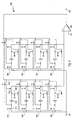
- the circuit arrangement 300 of Fig. 3 comprises an input line 301 and N parallel SC samplers, where N is a positive integer, for graphical clarity only three parallel SC samplers 302, 303 and 304 are shown. Consistently with the prior arl SC samplers each SC sampler 302 to 304 comprises a controllable switch S and a capacitor C. In the model of an SC sampler used here as an example, the switch S is connected between the input and output of the SC sampler and the capacitor C is connected between the output of the SC sampler and a constant reference potential, which is usually the local ground potential as shown in Fig. 3.
- Controllable switch is a general denomination to any circuit arrangement between at least one input and at least one output, which has a conductive state and a nonconductive state and which can be selectively driven into one of the states by applying an electrical control signal.
- the input of each SC sampler is here connected directly to the input line 301 of the whole circuit arrangement.
- the circuit arrangement further comprises N controllable switches of which only the switches 305, 306 and 307 are shown. Of these N switches, each SC sampler has its own switch connected in series with the output of the SC sampler.
- Each of the N switches is further coupled to the input 308 of a buffering amplifier 309.
- the other input 310 of the buffering amplifier 309 is connected to a constant reference potential, here the ground potential.
- the output 311 of the buffering amplifier 309 is the same as the output of the whole circuit arrangement 300.
- a first clock signal f s is used to drive the sampling switches S.
- the first clock signal f s is a square wave signal containing regular consecutive pulses with zero rise time and zero decay time.
- a clock arrangement which is not shown in Fig.
- a second clock signal f s /N is used to simultaneously close and open all the N buffering switches connected in series with the outputs of the SC samplers, of which only buffering switches 305, 306 and 307 are shown.
- the frequency of the second clock signal f s /N is an integral fraction of the frequency of the first clock signal f s .
- the frequency of the second clock signal f s /N is obtained by dividing the frequency of the first clock signal f s by the number of the parallel SC samplers.
- the second clock signal is also ideally a square wave signal containing consecutive pulses, there is one pulse in the second clock signal during each cycle of N pulses in the first clock signal f s .
- the mutual phasing of the first and second clock signals will be explained in more detail below.
- the circuit arrangement of Fig. 3 functions as follows.
- An oscillating input signal is applied to input line 301 and consequently coupled to the input of each parallel SC sampler.
- the sampling switch S of the first SC sampler 302 is closed for the duration of one clock pulse of the first clock signal f s , resulting in a first sample of the input signal being taken and stored in the first SC sampler 302.
- a second sample is taken and stored by the second SC sampler 303 and so on until in the end of the cycle of N pulses a total of N separate samples have been taken and stored in the parallel SC samplers.
- the buffering switches 305, 306, 307 (and all other N-3 buffering switches) are closed simultaneously, causing all the separate samples to be summed together. The sum of all samples is thereby coupled to the first input 308 of the buffering amplifier 309. During the next cycle of N pulses in the first clock signal f s the output of the amplifier 309 will remain essentially constant, consistently with the buffering role of the amplifier.
- NF TOT B n Nf N NF LNA + NF mix - 1 G LNA , where the number N of parallel SC samplers now appears in the denominator of the first term (not to be confused with the N 's in NF TOT , NF LNA and NF mix ).
- the magnitude of the original term B n /f N caused by noise aliasing is significantly reduced even for relatively small N.
- Fig. 4 is a Z-domain representation 400 of the arrangement of Fig. 3.
- input point 401 corresponds to input line 301 of Fig. 3 and the N multiplication elements Z -1 , of which only the two first elements 402 and 403 are shown, correspond to the N parallel SC samplers.
- the outputs of the multiplication elements are combined in adder 405 and the result of the addition is coupled to the decimator 406 which corresponds to the sample rate reduction in the buffer amplifier 309 of Fig. 3.
- FIR Finite Impulse Response
- Fig. 4a illustrates the transfer function of one such filter with 4 taps; in Fig. 4a the vertical axis corresponds to gain in decibels and the transmission zeroes are clearly visible.
- Fig. 5 illustrates a simplified schematic of a practical circuit 500 that can be used to implement the novel and inventive idea presented above.
- input line 501 corresponds to input line 301 of Fig. 3 and output line 502 corresponds to output line 311 of Fig. 3.
- Amplifier 509 is easily seen to correspond to amplifier 309 of Fig. 3.
- the first SC sampler 510 is used as an example.
- the SC sampler 510 comprises two synchronously operating first switches 511 and 512, which together form the sampling switch.
- the signal that controls the operation of the switches 511 and 512 is denoted as 51.
- the SC sampler further comprises a capacitor 513 and two synchronously operating second switches 514 and 515. which together form the buffering switch.
- the signal that controls the operation of the switches 514 and 515 is denoted as A.
- the control inputs for the signals that open and close the switches are not physically shown. However, it is obvious to the person skilled in the art how such inputs are built into switching arrangements handling high-frequency signals.
- Switch 511 is located between the input of the SC sampler 510 and the first plate of the capacitor 513.
- Switch 512 is located between the second plate of capacitor 513 and ground.
- Switch 514 is located between the second plate of capacitor 5 13 and the output of the SC sampler 510 and switch 515 is located between the first plate of capacitor 513 and the output of amplifier 509.
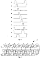
- SC samplers 550 to 580 All other SC samplers are similar to the SC sampler 510 described above, with the exception that in SC samplers 550 to 580 a signal B is used to control the buffering switches instead of signal A as in SC samplers 510 to 540. Also, each SC sampler 510 to 580 has its own signal 51 to 58 respectively for controlling the sampling switch.
- Fig. 6 is a timing diagram that shows the mutual relations in time of signals 51 to 58 that control the operation of the sampling switches as well as signals A and B that control the operation of the buffering switches. It is easily seen that the clock pulses that close and open the sampling switches are given consecutively to each SC sampler so that the duration in time of one clock pulse is one fourth of the sampling cycle.
- the sampling cycle may be understood as the period during which one sample is produced at the output of the buffering component; according to Fig. 6 this happens always after the taking of four consecutive samples at the input.
- the clock generator goes through eight states during the sampling cycle.
- a sampling and storing cycle is on in SC samplers 550 to 580.
- the circuit of Fig. 5 does not take the sum of the samples at the buffering stage but their mean value. In this case it is conceptually more or less the same because the parallel SC sampler branches are equally weighted in taking the mean value.
- This invention is not limited in taking the sum or exact mean value of the samples, although the term "summing" is used for brevity. A more general description of the process would be taking some previously determined combination of the samples.
- the minimum number of separate SC samplers that would be required to implement a circuit where the sampling and buffering operations do not take place simultaneously would actually be six; in general to implement the principle of Fig. 3 for any N the minimum number of SC samplers is considered to be 3N/2.
- the invention does not limit the number of separate SC samplers and their grouping. However, the generation of clock signals is very straightforward with an arrangement of 2N SC samplers arranged in two groups like the two times four SC arrangement in Fig. 5.
- the invention does not restrict the exact timing of the buffering operation in relation to the sampling operations, as long as it can be assured that the buffering (the "reading" of the samples) does not interfere with the sampling itself.
- the invention does not restrict the generation of clock signals for the SC samplers.
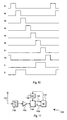
- Fig. 7 shows one exemplary way of producing clock signals to eight SC samplers.
- the clock signal generator 700 comprises eight D-flipflops 701 to 708 in series and eight switch drivers 711 to 718 connected so that each D-flipflop provides the enabling signal EN to one switch driver from its output Q.
- the output Q of each D-flipflop is also coupled to the input D of the next D-flipflop and the output Q of the last D-flipflop 708 is coupled to the input D of the first D-flipflop 701.
- a clock signal CK is coupled to the signal input of the switch drivers 711 to 718 and the inverse CK of the clock signal is coupled to the clock input CLK of the D-flipflops 701 to 708.
- a clock signal for one SC sampler is obtained.
- the flip-flops must be initialized during a reset period so that one of them is set to logical '1' and the others are set to logical '0'.
- the input frequency that will be sampled with a sampling mixer may be limited by other aspects than the achievable clock frequency that was discussed previously. If a prior art sampling mixer according to Fig. 2 is used to downconvert a very high intermediate frequency, the nonlinear switch resistance or the nonlinear switch capacitances inherently associated with the high-frequency switch 203 may give rise to unacceptable distortion in the sampler track-mode. Therefore it may be desirable to use the lowest possible IF determined by the system requirements and raise the sampling frequency above the IF. However, in this case downconversion to baseband can no longer be performed by sampling with a conventional arrangement.
- a further application of the basic inventive idea described above may be presented.
- This further application is based on the suitable multiplication (advantageously inversion) of selected samples before summing them together with the rest of the samples.
- Fig. 8 illustrates this principle applied to a circuit arrangement which has the additional feature that all signals are differential; the considerations of differential signals can as such be applied also to the arrangements according to Figs. 3 and 5. Inverting a number of selected samples is especially easy when the signals are in differential form, but the general idea of inverting does not require the signals to be differential.
- the circuit arrangement 800 of Fig. 8 comprises a differential input consisting of a first input line 801 and a second input line 802 for inputting a signal as an oscillating potential difference between the two input lines.
- N parallel SC samplers connected to the input lines 801 and 802, of which only SC samplers 803 to 806 are shown.
- the internal structure of an SC sampler is illustrated more closely in Fig. 8a.
- the SC samplers have two inputs I1 and I2 and two outputs O1 and O2 for handling differential signals.
- switches S1 and S2 each one of them being located between one input and the corresponding output.
- Each SC sampler also comprises two capacitors C1 and C2, each one of them being located between one output and a constant reference potential, which is most advantageously the ground potential.
- the two switches S1 and S2 function synchronously with each other as a response to a first control signal.
- the circuit arrangement 800 additionally comprises 2N buffering switches of which only buffering switches 811 to 818 are shown. All buffering switches operate synchronously with each other as a response to a second control signal.
- the buffering switches are arranged in pairs so that buffering switches 811 and 812 are coupled between the outputs of SC sampler 803 and the inputs of buffering amplifier 809, buffering switches 813 and 814 are coupled between the outputs of SC sampler 804 and the inputs of buffering amplifier 809 and so on.
- FIG. 8 the output wires of SC samplers 804 and 806 are cross-connected, meaning that the second output of each of these SC samplers is coupled - via the respective buffering switch - to the first input of amplifier 809 and the first output of the SC sampler is coupled - via the respective buffering switch - to the second input of amplifier 809. It has no importance whether the cross-connection takes physically place before or after the buffering switches. The inversion of the samples may be done even before sampling but this may introduce mismatch between signal paths.
- the roles of the first and second control signals in Fig. 8 are the same as those of the first and second clock signals in Fig. 3. Namely, the first control signal contains regular clock pulses at a relatively high frequency, and a clocking arrangement not shown in Fig. 8 will arrange the conduction of said clock pulses cyclically so that during a sampling cycle of N consecutive clock pulses each SC sampler will receive a clock pulse of its own. After the sampling cycle has been completed, a pulse in the second control signal will close the buffering switches, whereby the sum of the samples collected in the SC samplers is read into the buffering amplifier. For enabling continuous sampling that does not interfere with the buffering, many kinds of groupings of the SC samplers is possible; reference is made here to the exemplary grouping of two times four in Fig. 5.
- IQ-phasing may be generated simply by sampling at four times the input frequency and passing every even sample to the I-branch and every odd sample to the Q-branch of the receiver.
- the above-explained principle is illustrated in Fig. 9, which depicts a practical circuit arrangement that can be used to implement the currently discussed further application of the invention.
- the circuit arrangement 900 comprises two physical input lines 901 and 902 which are, as in Fig. 8, actually only the two halves of a single logical input line for differential signals.
- SC samplers 910 to 980 there are eight SC samplers 910 to 980, but is has to be noted that the previous disclaimers about the invention not limiting the number of parallel SC samplers again apply.
- the SC samplers 910, 930, 950 and 970 belong to the I-branch group and the SC samplers 920, 940, 960 and 980 belong to the Q-branch group; if the concept of Fig.
- SC sampler 9 is generalised to include any number of parallel SC samplers, it is most advantageous that there are always as many SC samplers in the I-branch group as in the Q-branch group and that the number of SC samplers in each group is even, although this is not necessary.
- the internal structure of the SC samplers is identical to that described above in connection with Figs. 8 and 8a.
- Each SC sampler has two inputs (i.e. a differential input) which are connected to input lines 901 and 902.
- Each SC sampler has also two outputs (i.e. a differential output).
- the outputs of the SC samplers in the I-branch group are coupled - via their respective buffering switches - to the inputs of the I-branch buffering amplifier 903 and the outputs of the SC samplers in the Q-branch group are coupled - via their respective buffering switches - to the inputs of the Q-branch buffering amplifier 904.
- the outputs of the SC samplers 930, 970, 940 and 980 are cross-connected before coupling them to the inputs of the respective buffering amplifiers. In Fig. 9 the cross-connection takes place physically before the buffering switches; it could as well take place between the buffering switches and the buffering amplifiers.
- a first buffering signal A is used to control the operation of the buffering switches 914, 915, 934, 935, 924, 925, 944 and 945.
- a second buffering signal B is used to control the operation of the buffering switches 954, 955, 974, 975, 964, 965, 984 and 985.
- the first control signals that control the operation of the sampling switches in SC samplers 910 to 980 are numbered from 91 to 98 respectively.
- the timing diagram of Fig. 10 illustrates the mutual timing of the control signals.
- the sampling time base, from which the control signals 91 to 98 are derived has the frequency of four times the input frequency
- the buffering frequency time base from which the control signals A and B are derived, has the same frequency as the input frequency.
- input frequency it is meant the frequency of interest that is coupled to input lines 901 and 902 during the operation of the circuit. If the apparatus of Fig. 9 is used for downconversion from intermediate frequency to baseband, the input frequency is the same as the
- the input frequency is an intermediate frequency in a radio receiver.
- the sampling frequency seen in each branch (I or Q branch) alone is two times the intermediate frequency, which relaxes the anti-alias filtering and sampling jitter requirements as discussed previously.
- the sampling clock or any of its harmonics do not operate on the LO frequency and it is located out of the antialias filter passband.
- the driving circuit sees similar disturbances from the I- and Q sampling clocks which results in good IQ-balance. Additionally, any DC-component passing the sampler (coming with the IF signal or generated by the sampler arrangement) is blocked by the transmission zero at DC.
- the same technique can be used in a subsampling mixer converting a bandlimited RF signal to baseband.
- the RF signal would be first converted to IF by sampling and immediately moved to baseband by the subsequent decimation operation. This kind of downconversion could be called quasi-direct, because there would be no analogue signal processing (filtering or amplification) at the IF.
- the RF signal in the sampler input would be converted directly to baseband in the cross-coupled sampling downconverter block, and the rest of the signal processing could be done at the baseband.
- a similar image problem should be accounted for as in a superheterodyne receiver.
- the further application discussed above with reference to Figs. 8 - 10 is not limited to just inverting selected samples.
- the fundamental idea of the further application is to modify the coefficients determining the FIR transfer function. This way the transmission zeroes can be chosen so that during decimation only a narrow frequency band folds down to DC.
- the coefficients need thus not be exactly - 1 and 1 as in the inversion case, although that is an advantageous selection of coefficients because it maximises the conversion gain.
- the relation of the clock frequency to the intermediate frequency does not need to be an even number. Downconverting for example from a frequency that is one third of the Nyquist frequency, taking the coefficients to be 0.5, -1 and 0.5 and decimating by three would be one working solution.
- Fig. 11 illustrates a receiver 1100 where the present invention is utilized.
- a radio frequency signal picked up by the antenna 1101 is filtered in a band pass filter 1102 and amplified in a Low Noise Amplifier (LNA) 1103 before conducting it to a cross-coupled sampling downconverter block 1104 according to the invention.
- the output from block 1103 is a baseband signal on two branches 1105 and 1106. It is conducted to a baseband signal processing block 1107 which can be a known baseband block with any combination of the known functions for reconstructing the information content of a received signal and possibly presenting it to a user in the form of audible signal and/or on a display.
- Oscillator block 1108 provides the cross-coupled sampling downconverter block 1104 with the necessary clock signals and it may operate under the control of a microprocessor included in the baseband signal processing block 1107.
Landscapes
- Engineering & Computer Science (AREA)
- Power Engineering (AREA)
- Physics & Mathematics (AREA)
- Computer Hardware Design (AREA)
- Mathematical Physics (AREA)
- Analogue/Digital Conversion (AREA)
- Processing Of Color Television Signals (AREA)
- Color Television Systems (AREA)
- Transmission Systems Not Characterized By The Medium Used For Transmission (AREA)
Applications Claiming Priority (2)
| Application Number | Priority Date | Filing Date | Title |
|---|---|---|---|
| FI981209A FI120124B (fi) | 1998-05-29 | 1998-05-29 | Menetelmä ja piiri signaalin näytteistämiseksi suurella näytteistystaajuudella |
| FI981209 | 1998-05-29 |
Publications (2)
| Publication Number | Publication Date |
|---|---|
| EP0961406A2 true EP0961406A2 (fr) | 1999-12-01 |
| EP0961406A3 EP0961406A3 (fr) | 1999-12-29 |
Family
ID=8551847
Family Applications (1)
| Application Number | Title | Priority Date | Filing Date |
|---|---|---|---|
| EP99660088A Withdrawn EP0961406A3 (fr) | 1998-05-29 | 1999-05-25 | Procédé et circuit d'échantillonnage d'un signal à haute fréquence d'échantillonage |
Country Status (3)
| Country | Link |
|---|---|
| US (1) | US6438366B1 (fr) |
| EP (1) | EP0961406A3 (fr) |
| FI (1) | FI120124B (fr) |
Cited By (2)
| Publication number | Priority date | Publication date | Assignee | Title |
|---|---|---|---|---|
| US6847689B1 (en) | 1999-12-16 | 2005-01-25 | Nokia Mobile Phones Ltd. | Method for distinguishing signals from one another, and filter |
| WO2006039949A1 (fr) * | 2004-10-12 | 2006-04-20 | Stmicroelectronics Sa | Procede permettant d'echantillonner un signal rf analogique |
Families Citing this family (44)
| Publication number | Priority date | Publication date | Assignee | Title |
|---|---|---|---|---|
| US7515896B1 (en) | 1998-10-21 | 2009-04-07 | Parkervision, Inc. | Method and system for down-converting an electromagnetic signal, and transforms for same, and aperture relationships |
| US6061551A (en) * | 1998-10-21 | 2000-05-09 | Parkervision, Inc. | Method and system for down-converting electromagnetic signals |
| US7236754B2 (en) | 1999-08-23 | 2007-06-26 | Parkervision, Inc. | Method and system for frequency up-conversion |
| US6813485B2 (en) * | 1998-10-21 | 2004-11-02 | Parkervision, Inc. | Method and system for down-converting and up-converting an electromagnetic signal, and transforms for same |
| US7039372B1 (en) | 1998-10-21 | 2006-05-02 | Parkervision, Inc. | Method and system for frequency up-conversion with modulation embodiments |
| US7027786B1 (en) | 1998-10-21 | 2006-04-11 | Parkervision, Inc. | Carrier and clock recovery using universal frequency translation |
| US6370371B1 (en) | 1998-10-21 | 2002-04-09 | Parkervision, Inc. | Applications of universal frequency translation |
| US6542722B1 (en) | 1998-10-21 | 2003-04-01 | Parkervision, Inc. | Method and system for frequency up-conversion with variety of transmitter configurations |
| US7209725B1 (en) | 1999-01-22 | 2007-04-24 | Parkervision, Inc | Analog zero if FM decoder and embodiments thereof, such as the family radio service |
| US6873836B1 (en) | 1999-03-03 | 2005-03-29 | Parkervision, Inc. | Universal platform module and methods and apparatuses relating thereto enabled by universal frequency translation technology |
| US6853690B1 (en) | 1999-04-16 | 2005-02-08 | Parkervision, Inc. | Method, system and apparatus for balanced frequency up-conversion of a baseband signal and 4-phase receiver and transceiver embodiments |
| US6879817B1 (en) | 1999-04-16 | 2005-04-12 | Parkervision, Inc. | DC offset, re-radiation, and I/Q solutions using universal frequency translation technology |
| US7110435B1 (en) | 1999-03-15 | 2006-09-19 | Parkervision, Inc. | Spread spectrum applications of universal frequency translation |
| US7693230B2 (en) | 1999-04-16 | 2010-04-06 | Parkervision, Inc. | Apparatus and method of differential IQ frequency up-conversion |
| US7065162B1 (en) | 1999-04-16 | 2006-06-20 | Parkervision, Inc. | Method and system for down-converting an electromagnetic signal, and transforms for same |
| US7110444B1 (en) | 1999-08-04 | 2006-09-19 | Parkervision, Inc. | Wireless local area network (WLAN) using universal frequency translation technology including multi-phase embodiments and circuit implementations |
| US8295406B1 (en) * | 1999-08-04 | 2012-10-23 | Parkervision, Inc. | Universal platform module for a plurality of communication protocols |
| SE9903532D0 (sv) * | 1999-09-28 | 1999-09-28 | Jiren Yuan | Versatile charge sampling circuits |
| US7082171B1 (en) | 1999-11-24 | 2006-07-25 | Parkervision, Inc. | Phase shifting applications of universal frequency translation |
| US6959049B2 (en) * | 2000-04-10 | 2005-10-25 | Texas Instruments Incorporated | Multi-tap, digital-pulse-driven mixer |
| US7010286B2 (en) | 2000-04-14 | 2006-03-07 | Parkervision, Inc. | Apparatus, system, and method for down-converting and up-converting electromagnetic signals |
| US6829003B2 (en) * | 2000-06-02 | 2004-12-07 | Pentax Corporation | Sampling pulse generator of electronic endoscope |
| US7554508B2 (en) | 2000-06-09 | 2009-06-30 | Parker Vision, Inc. | Phased array antenna applications on universal frequency translation |
| US7454453B2 (en) | 2000-11-14 | 2008-11-18 | Parkervision, Inc. | Methods, systems, and computer program products for parallel correlation and applications thereof |
| US7010559B2 (en) | 2000-11-14 | 2006-03-07 | Parkervision, Inc. | Method and apparatus for a parallel correlator and applications thereof |
| US7356069B2 (en) * | 2001-04-25 | 2008-04-08 | Texas Instruments Incorporated | Spread spectrum demodulation using a subsampling communication receiver architecture |
| US6963732B2 (en) * | 2001-04-25 | 2005-11-08 | Texas Instruments Incorporated | Subsampling communication receiver architecture with relaxed IFA readout timing |
| US7003276B2 (en) * | 2001-04-25 | 2006-02-21 | Texas Instruments Incorporated | Subsampling communication receiver architecture with gain control and RSSI generation |
| US8027657B2 (en) * | 2001-10-26 | 2011-09-27 | Texas Instruments Incorporated | Sampling mixer with asynchronous clock and signal domains |
| US6643171B2 (en) * | 2001-11-06 | 2003-11-04 | Winbond Electronics Corporation | High dynamic range recording and playback for multilevel storage using differential sampling |
| US7072427B2 (en) | 2001-11-09 | 2006-07-04 | Parkervision, Inc. | Method and apparatus for reducing DC offsets in a communication system |
| US7321640B2 (en) * | 2002-06-07 | 2008-01-22 | Parkervision, Inc. | Active polyphase inverter filter for quadrature signal generation |
| US7460584B2 (en) * | 2002-07-18 | 2008-12-02 | Parkervision, Inc. | Networking methods and systems |
| US7379883B2 (en) | 2002-07-18 | 2008-05-27 | Parkervision, Inc. | Networking methods and systems |
| US7197524B2 (en) * | 2003-05-29 | 2007-03-27 | Texas Instruments Incorporated | Direct RF sampling for cable applications and other broadband signals |
| JP4306515B2 (ja) * | 2003-08-29 | 2009-08-05 | 株式会社デンソー | 同期検波方法及び装置 |
| US7558351B2 (en) * | 2004-02-10 | 2009-07-07 | Wionics Research | Super harmonic filter and method of filtering frequency components from a signal |
| US7339509B2 (en) * | 2006-05-02 | 2008-03-04 | Agilent Technologies, Inc. | Sampling system using sampling apertures of different durations |
| US8000426B2 (en) * | 2008-03-21 | 2011-08-16 | Oracle America, Inc. | Mechanism for constructing an oversampled waveform for a set of signals received by a receiver |
| US7994850B2 (en) * | 2008-06-25 | 2011-08-09 | Qualcomm, Incorporated | Discrete time multi-rate analog filter |
| US9568581B2 (en) * | 2012-07-16 | 2017-02-14 | Fujitsu Limited | Signal sampler with a calibration circuit |
| US8838055B2 (en) | 2012-11-30 | 2014-09-16 | Motorola Solutions, Inc. | Dynamic sub-sampling radio frequency mixer systems and methods |
| EP2974008B1 (fr) * | 2013-03-15 | 2021-01-27 | Hae-Seung Lee | Circuit d'amplificateur tampon |
| JP2015100042A (ja) * | 2013-11-19 | 2015-05-28 | 株式会社東芝 | ノイズ除去装置、および撮像装置 |
Family Cites Families (29)
| Publication number | Priority date | Publication date | Assignee | Title |
|---|---|---|---|---|
| US4253067A (en) * | 1978-12-11 | 1981-02-24 | Rockwell International Corporation | Baseband differentially phase encoded radio signal detector |
| CA1233890A (fr) | 1985-05-27 | 1988-03-08 | Peter Gillingham | Filtre decimateur |
| JPS63318811A (ja) * | 1987-06-22 | 1988-12-27 | Toshiba Corp | ディジタルフィルタ装置 |
| FI91337C (fi) | 1990-04-27 | 1994-06-10 | Nokia Mobile Phones Ltd | Kytkentäjärjestely harhatoiston eliminoimiseksi radiopuhelimen vastaanottimessa |
| FI86120C (fi) | 1990-07-02 | 1992-07-10 | Nokia Mobile Phones Ltd | A/d- eller d/a-omvandlare, a/d- eller d/a-omvandlarsystem samt kalibreringsfoerfarande foer dessa. |
| US5134403A (en) | 1990-12-06 | 1992-07-28 | Hewlett-Packard Co. | High speed sampling and digitizing system requiring no hold circuit |
| FI88980C (fi) | 1991-01-09 | 1993-07-26 | Nokia Mobile Phones Ltd | Sigma-delta-modulator foer d/a-omvandlare |
| US5162723A (en) | 1991-02-11 | 1992-11-10 | Hewlett-Packard Company | Sampling signal analyzer |
| FI88765C (fi) | 1991-04-09 | 1993-06-28 | Nokia Mobile Phones Ltd | Foerfarande och arrangemang foer stabilering av en hoegre grads sigma-delta-modulator |
| US5303404A (en) | 1991-10-17 | 1994-04-12 | Nokia Mobile Phones Ltd. | Adjustable bandwidth in a radiotelephone |
| FI95853C (fi) | 1991-11-08 | 1996-03-25 | Nokia Mobile Phones Ltd | Menetelmä D/A-muuntimen offset-jännitteiden vaihteluiden vaikutuksen korjaamiseksi muuntimen lähtöjännitteestä |
| FI98580C (fi) | 1991-11-14 | 1997-07-10 | Nokia Mobile Phones Ltd | Selektiivisyyssuodatus solukkopuhelimessa |
| GB9318640D0 (en) * | 1993-09-08 | 1993-10-27 | Philips Electronics Uk Ltd | Integrator |
| FI107855B (fi) | 1993-09-10 | 2001-10-15 | Nokia Mobile Phones Ltd | Vt-signaalin demodulointi sigma-delta-muuntimella |
| FI96811C (fi) | 1993-11-30 | 1996-08-26 | Nokia Mobile Phones Ltd | Menetelmä ja piirijärjestely D/A-muuntimen DC-erojännitteen kompensoimiseksi |
| FI950106L (fi) | 1995-01-10 | 1996-07-11 | Nokia Mobile Phones Ltd | Menetelmä ja kytkentä häiriöiden suodattamiseksi radiolaitteen vastaanottimessa |
| FI98020C (fi) | 1995-06-06 | 1997-03-25 | Nokia Mobile Phones Ltd | Digitaalisen signaalin modulointimenetelmä ja modulaattori |
| FI101027B (fi) | 1996-01-05 | 1998-03-31 | Nokia Mobile Phones Ltd | Multipleksoitu signaalimuunnos |
| GB2310115B (en) * | 1996-02-08 | 2000-06-07 | Nokia Mobile Phones Ltd | Method and apparatus for dc compensation |
| US6037887A (en) * | 1996-03-06 | 2000-03-14 | Burr-Brown Corporation | Programmable gain for delta sigma analog-to-digital converter |
| US5691720A (en) * | 1996-03-08 | 1997-11-25 | Burr- Brown Corporation | Delta sigma analog-to-digital converter having programmable resolution/bias current circuitry and method |
| US5892540A (en) | 1996-06-13 | 1999-04-06 | Rockwell International Corporation | Low noise amplifier for passive pixel CMOS imager |
| US5909131A (en) * | 1996-07-31 | 1999-06-01 | Analog Devices, Inc. | Low-distortion technique to bandlimit a switched-capacitor sampling circuit |
| US5914638A (en) * | 1997-06-06 | 1999-06-22 | Omnivision Technologies, Inc. | Method and apparatus for adjusting the common-mode output voltage of a sample-and-hold amplifier |
| US6061008A (en) * | 1997-12-19 | 2000-05-09 | Rockwell Science Center, Inc. | Sigma-delta-sigma modulator for high performance analog-to-digital and digital-to-analog conversion |
| US6243430B1 (en) * | 1998-01-09 | 2001-06-05 | Qualcomm Incorporated | Noise cancellation circuit in a quadrature downconverter |
| US6100834A (en) * | 1998-05-15 | 2000-08-08 | Pairgain Technologies, Inc. | Recursive multi-bit ADC with predictor |
| US6215337B1 (en) * | 1999-01-12 | 2001-04-10 | Qualcomm Incorporated | Linear sampling switch |
| US6194940B1 (en) * | 1999-09-27 | 2001-02-27 | Lucent Technologies Inc. | Automatic clock switching |
-
1998
- 1998-05-29 FI FI981209A patent/FI120124B/fi not_active IP Right Cessation
-
1999
- 1999-05-21 US US09/316,357 patent/US6438366B1/en not_active Expired - Lifetime
- 1999-05-25 EP EP99660088A patent/EP0961406A3/fr not_active Withdrawn
Cited By (3)
| Publication number | Priority date | Publication date | Assignee | Title |
|---|---|---|---|---|
| US6847689B1 (en) | 1999-12-16 | 2005-01-25 | Nokia Mobile Phones Ltd. | Method for distinguishing signals from one another, and filter |
| WO2006039949A1 (fr) * | 2004-10-12 | 2006-04-20 | Stmicroelectronics Sa | Procede permettant d'echantillonner un signal rf analogique |
| US7634247B2 (en) | 2004-10-12 | 2009-12-15 | Stmicroelectronics S.A. | Method of sampling an analogue radiofrequency signal |
Also Published As
| Publication number | Publication date |
|---|---|
| FI120124B (fi) | 2009-06-30 |
| FI981209A0 (fi) | 1998-05-29 |
| EP0961406A3 (fr) | 1999-12-29 |
| US20020098823A1 (en) | 2002-07-25 |
| FI981209L (fi) | 1999-11-30 |
| US6438366B1 (en) | 2002-08-20 |
Similar Documents
| Publication | Publication Date | Title |
|---|---|---|
| US6438366B1 (en) | Method and circuit for sampling a signal at high sampling frequency | |
| US6101226A (en) | Radio receiving apparatus for receiving communication signals of different bandwidths | |
| US7079826B2 (en) | Digitally controlled analog RF filtering in subsampling communication receiver architecture | |
| US6459743B1 (en) | Digital reception with radio frequency sampling | |
| JP3392670B2 (ja) | サンプリング装置 | |
| US4972436A (en) | High performance sigma delta based analog modem front end | |
| US8542616B2 (en) | Simultaneous multiple signal reception and transmission using frequency multiplexing and shared processing | |
| JP5078988B2 (ja) | 離散時間ダイレクトサンプリング回路及び受信機 | |
| Poberezhskiy et al. | Sampling and signal reconstruction circuits performing internal antialiasing filtering and their influence on the design of digital receivers and transmitters | |
| US7003276B2 (en) | Subsampling communication receiver architecture with gain control and RSSI generation | |
| CN111431483B (zh) | 用于从输入信号产生输出信号的混频器和方法 | |
| US7514993B2 (en) | IQ demodulator | |
| US7979047B2 (en) | Sampling filter | |
| US6388600B1 (en) | Asynchronous superconductor serial multiply-accumulator | |
| US7356069B2 (en) | Spread spectrum demodulation using a subsampling communication receiver architecture | |
| US6647075B1 (en) | Digital tuner with optimized clock frequency and integrated parallel CIC filter and local oscillator | |
| US6963732B2 (en) | Subsampling communication receiver architecture with relaxed IFA readout timing | |
| US20090257531A1 (en) | Sampling filter apparatus and wireless communication apparatus | |
| US7634247B2 (en) | Method of sampling an analogue radiofrequency signal | |
| CN118523785B (zh) | 一种具备亚采样功能的超再生接收机 | |
| Lindfors et al. | A novel technique for noise reduction in CMOS subsamplers | |
| Poberezhskiy et al. | Influence of non-ideal integration on sampling circuits with internal antialiasing filtering |
Legal Events
| Date | Code | Title | Description |
|---|---|---|---|
| PUAI | Public reference made under article 153(3) epc to a published international application that has entered the european phase |
Free format text: ORIGINAL CODE: 0009012 |
|
| PUAL | Search report despatched |
Free format text: ORIGINAL CODE: 0009013 |
|
| AK | Designated contracting states |
Kind code of ref document: A2 Designated state(s): DE FR GB IT |
|
| AX | Request for extension of the european patent |
Free format text: AL;LT;LV;MK;RO;SI |
|
| AK | Designated contracting states |
Kind code of ref document: A3 Designated state(s): AT BE CH CY DE DK ES FI FR GB GR IE IT LI LU MC NL PT SE |
|
| AX | Request for extension of the european patent |
Free format text: AL;LT;LV;MK;RO;SI |
|
| 17P | Request for examination filed |
Effective date: 20000505 |
|
| AKX | Designation fees paid |
Free format text: DE FR GB IT |
|
| RAP1 | Party data changed (applicant data changed or rights of an application transferred) |
Owner name: NOKIA CORPORATION |
|
| 17Q | First examination report despatched |
Effective date: 20080402 |
|
| RAP1 | Party data changed (applicant data changed or rights of an application transferred) |
Owner name: NOKIA CORPORATION |
|
| RAP1 | Party data changed (applicant data changed or rights of an application transferred) |
Owner name: NOKIA TECHNOLOGIES OY |
|
| STAA | Information on the status of an ep patent application or granted ep patent |
Free format text: STATUS: THE APPLICATION IS DEEMED TO BE WITHDRAWN |
|
| 18D | Application deemed to be withdrawn |
Effective date: 20171201 |