EP0962957A2 - Lichtemittierende Anzeigevorrichtungen - Google Patents
Lichtemittierende Anzeigevorrichtungen Download PDFInfo
- Publication number
- EP0962957A2 EP0962957A2 EP99304377A EP99304377A EP0962957A2 EP 0962957 A2 EP0962957 A2 EP 0962957A2 EP 99304377 A EP99304377 A EP 99304377A EP 99304377 A EP99304377 A EP 99304377A EP 0962957 A2 EP0962957 A2 EP 0962957A2
- Authority
- EP
- European Patent Office
- Prior art keywords
- diamond
- emitter
- metal
- voltage
- light
- Prior art date
- Legal status (The legal status is an assumption and is not a legal conclusion. Google has not performed a legal analysis and makes no representation as to the accuracy of the status listed.)
- Withdrawn
Links
- 239000000758 substrate Substances 0.000 claims abstract description 10
- 239000010432 diamond Substances 0.000 description 33
- 229910003460 diamond Inorganic materials 0.000 description 33
- 229910052751 metal Inorganic materials 0.000 description 17
- 239000002184 metal Substances 0.000 description 17
- 238000000034 method Methods 0.000 description 9
- OAICVXFJPJFONN-UHFFFAOYSA-N Phosphorus Chemical compound [P] OAICVXFJPJFONN-UHFFFAOYSA-N 0.000 description 8
- UFHFLCQGNIYNRP-UHFFFAOYSA-N Hydrogen Chemical compound [H][H] UFHFLCQGNIYNRP-UHFFFAOYSA-N 0.000 description 5
- RYGMFSIKBFXOCR-UHFFFAOYSA-N Copper Chemical compound [Cu] RYGMFSIKBFXOCR-UHFFFAOYSA-N 0.000 description 4
- 229910052802 copper Inorganic materials 0.000 description 4
- 239000010949 copper Substances 0.000 description 4
- 239000001257 hydrogen Substances 0.000 description 4
- 229910052739 hydrogen Inorganic materials 0.000 description 4
- 239000000843 powder Substances 0.000 description 4
- 239000003054 catalyst Substances 0.000 description 3
- ZOKXTWBITQBERF-UHFFFAOYSA-N Molybdenum Chemical compound [Mo] ZOKXTWBITQBERF-UHFFFAOYSA-N 0.000 description 2
- PXHVJJICTQNCMI-UHFFFAOYSA-N Nickel Chemical compound [Ni] PXHVJJICTQNCMI-UHFFFAOYSA-N 0.000 description 2
- XUIMIQQOPSSXEZ-UHFFFAOYSA-N Silicon Chemical compound [Si] XUIMIQQOPSSXEZ-UHFFFAOYSA-N 0.000 description 2
- RTAQQCXQSZGOHL-UHFFFAOYSA-N Titanium Chemical compound [Ti] RTAQQCXQSZGOHL-UHFFFAOYSA-N 0.000 description 2
- 239000011230 binding agent Substances 0.000 description 2
- 238000000151 deposition Methods 0.000 description 2
- 238000010438 heat treatment Methods 0.000 description 2
- 150000001247 metal acetylides Chemical class 0.000 description 2
- VNWKTOKETHGBQD-UHFFFAOYSA-N methane Chemical compound C VNWKTOKETHGBQD-UHFFFAOYSA-N 0.000 description 2
- 229910052750 molybdenum Inorganic materials 0.000 description 2
- 239000011733 molybdenum Substances 0.000 description 2
- 239000002245 particle Substances 0.000 description 2
- 229910052710 silicon Inorganic materials 0.000 description 2
- 239000010703 silicon Substances 0.000 description 2
- 239000010936 titanium Substances 0.000 description 2
- 229910052719 titanium Inorganic materials 0.000 description 2
- 239000004215 Carbon black (E152) Substances 0.000 description 1
- VYZAMTAEIAYCRO-UHFFFAOYSA-N Chromium Chemical compound [Cr] VYZAMTAEIAYCRO-UHFFFAOYSA-N 0.000 description 1
- 229910001374 Invar Inorganic materials 0.000 description 1
- FYYHWMGAXLPEAU-UHFFFAOYSA-N Magnesium Chemical compound [Mg] FYYHWMGAXLPEAU-UHFFFAOYSA-N 0.000 description 1
- BQCADISMDOOEFD-UHFFFAOYSA-N Silver Chemical compound [Ag] BQCADISMDOOEFD-UHFFFAOYSA-N 0.000 description 1
- 238000005299 abrasion Methods 0.000 description 1
- 239000004411 aluminium Substances 0.000 description 1
- 229910052782 aluminium Inorganic materials 0.000 description 1
- XAGFODPZIPBFFR-UHFFFAOYSA-N aluminium Chemical compound [Al] XAGFODPZIPBFFR-UHFFFAOYSA-N 0.000 description 1
- PNEYBMLMFCGWSK-UHFFFAOYSA-N aluminium oxide Inorganic materials [O-2].[O-2].[O-2].[Al+3].[Al+3] PNEYBMLMFCGWSK-UHFFFAOYSA-N 0.000 description 1
- 238000003491 array Methods 0.000 description 1
- 229910052792 caesium Inorganic materials 0.000 description 1
- TVFDJXOCXUVLDH-UHFFFAOYSA-N caesium atom Chemical compound [Cs] TVFDJXOCXUVLDH-UHFFFAOYSA-N 0.000 description 1
- 230000003197 catalytic effect Effects 0.000 description 1
- 229910052804 chromium Inorganic materials 0.000 description 1
- 239000011651 chromium Substances 0.000 description 1
- 239000011248 coating agent Substances 0.000 description 1
- 238000000576 coating method Methods 0.000 description 1
- 239000002131 composite material Substances 0.000 description 1
- 238000011109 contamination Methods 0.000 description 1
- 238000007796 conventional method Methods 0.000 description 1
- 239000013078 crystal Substances 0.000 description 1
- 230000008021 deposition Effects 0.000 description 1
- 239000002019 doping agent Substances 0.000 description 1
- 238000010894 electron beam technology Methods 0.000 description 1
- 238000001962 electrophoresis Methods 0.000 description 1
- 239000007789 gas Substances 0.000 description 1
- 239000011521 glass Substances 0.000 description 1
- PCHJSUWPFVWCPO-UHFFFAOYSA-N gold Chemical compound [Au] PCHJSUWPFVWCPO-UHFFFAOYSA-N 0.000 description 1
- 229910052737 gold Inorganic materials 0.000 description 1
- 239000010931 gold Substances 0.000 description 1
- 229930195733 hydrocarbon Natural products 0.000 description 1
- 150000002430 hydrocarbons Chemical class 0.000 description 1
- 229910052746 lanthanum Inorganic materials 0.000 description 1
- FZLIPJUXYLNCLC-UHFFFAOYSA-N lanthanum atom Chemical compound [La] FZLIPJUXYLNCLC-UHFFFAOYSA-N 0.000 description 1
- 238000001459 lithography Methods 0.000 description 1
- 239000011777 magnesium Substances 0.000 description 1
- 229910052749 magnesium Inorganic materials 0.000 description 1
- 238000004519 manufacturing process Methods 0.000 description 1
- 239000000463 material Substances 0.000 description 1
- 229910044991 metal oxide Inorganic materials 0.000 description 1
- 150000004706 metal oxides Chemical class 0.000 description 1
- 239000000203 mixture Substances 0.000 description 1
- 229910052759 nickel Inorganic materials 0.000 description 1
- 229920002120 photoresistant polymer Polymers 0.000 description 1
- 238000009832 plasma treatment Methods 0.000 description 1
- 238000005498 polishing Methods 0.000 description 1
- 239000010453 quartz Substances 0.000 description 1
- VYPSYNLAJGMNEJ-UHFFFAOYSA-N silicon dioxide Inorganic materials O=[Si]=O VYPSYNLAJGMNEJ-UHFFFAOYSA-N 0.000 description 1
- 229910052709 silver Inorganic materials 0.000 description 1
- 239000004332 silver Substances 0.000 description 1
- 125000006850 spacer group Chemical group 0.000 description 1
- 239000000126 substance Substances 0.000 description 1
- 238000004381 surface treatment Methods 0.000 description 1
Images

Classifications
-
- C—CHEMISTRY; METALLURGY
- C23—COATING METALLIC MATERIAL; COATING MATERIAL WITH METALLIC MATERIAL; CHEMICAL SURFACE TREATMENT; DIFFUSION TREATMENT OF METALLIC MATERIAL; COATING BY VACUUM EVAPORATION, BY SPUTTERING, BY ION IMPLANTATION OR BY CHEMICAL VAPOUR DEPOSITION, IN GENERAL; INHIBITING CORROSION OF METALLIC MATERIAL OR INCRUSTATION IN GENERAL
- C23C—COATING METALLIC MATERIAL; COATING MATERIAL WITH METALLIC MATERIAL; SURFACE TREATMENT OF METALLIC MATERIAL BY DIFFUSION INTO THE SURFACE, BY CHEMICAL CONVERSION OR SUBSTITUTION; COATING BY VACUUM EVAPORATION, BY SPUTTERING, BY ION IMPLANTATION OR BY CHEMICAL VAPOUR DEPOSITION, IN GENERAL
- C23C16/00—Chemical coating by decomposition of gaseous compounds, without leaving reaction products of surface material in the coating, i.e. chemical vapour deposition [CVD] processes
- C23C16/22—Chemical coating by decomposition of gaseous compounds, without leaving reaction products of surface material in the coating, i.e. chemical vapour deposition [CVD] processes characterised by the deposition of inorganic material, other than metallic material
- C23C16/26—Deposition of carbon only
- C23C16/27—Diamond only
-
- H—ELECTRICITY
- H01—ELECTRIC ELEMENTS
- H01J—ELECTRIC DISCHARGE TUBES OR DISCHARGE LAMPS
- H01J9/00—Apparatus or processes specially adapted for the manufacture, installation, removal, maintenance of electric discharge tubes, discharge lamps, or parts thereof; Recovery of material from discharge tubes or lamps
- H01J9/02—Manufacture of electrodes or electrode systems
-
- B—PERFORMING OPERATIONS; TRANSPORTING
- B24—GRINDING; POLISHING
- B24D—TOOLS FOR GRINDING, BUFFING OR SHARPENING
- B24D18/00—Manufacture of grinding tools or other grinding devices, e.g. wheels, not otherwise provided for
-
- B—PERFORMING OPERATIONS; TRANSPORTING
- B82—NANOTECHNOLOGY
- B82Y—SPECIFIC USES OR APPLICATIONS OF NANOSTRUCTURES; MEASUREMENT OR ANALYSIS OF NANOSTRUCTURES; MANUFACTURE OR TREATMENT OF NANOSTRUCTURES
- B82Y10/00—Nanotechnology for information processing, storage or transmission, e.g. quantum computing or single electron logic
-
- C—CHEMISTRY; METALLURGY
- C09—DYES; PAINTS; POLISHES; NATURAL RESINS; ADHESIVES; COMPOSITIONS NOT OTHERWISE PROVIDED FOR; APPLICATIONS OF MATERIALS NOT OTHERWISE PROVIDED FOR
- C09K—MATERIALS FOR MISCELLANEOUS APPLICATIONS, NOT PROVIDED FOR ELSEWHERE
- C09K3/00—Materials not provided for elsewhere
- C09K3/14—Anti-slip materials; Abrasives
- C09K3/1409—Abrasive particles per se
-
- C—CHEMISTRY; METALLURGY
- C23—COATING METALLIC MATERIAL; COATING MATERIAL WITH METALLIC MATERIAL; CHEMICAL SURFACE TREATMENT; DIFFUSION TREATMENT OF METALLIC MATERIAL; COATING BY VACUUM EVAPORATION, BY SPUTTERING, BY ION IMPLANTATION OR BY CHEMICAL VAPOUR DEPOSITION, IN GENERAL; INHIBITING CORROSION OF METALLIC MATERIAL OR INCRUSTATION IN GENERAL
- C23C—COATING METALLIC MATERIAL; COATING MATERIAL WITH METALLIC MATERIAL; SURFACE TREATMENT OF METALLIC MATERIAL BY DIFFUSION INTO THE SURFACE, BY CHEMICAL CONVERSION OR SUBSTITUTION; COATING BY VACUUM EVAPORATION, BY SPUTTERING, BY ION IMPLANTATION OR BY CHEMICAL VAPOUR DEPOSITION, IN GENERAL
- C23C16/00—Chemical coating by decomposition of gaseous compounds, without leaving reaction products of surface material in the coating, i.e. chemical vapour deposition [CVD] processes
- C23C16/22—Chemical coating by decomposition of gaseous compounds, without leaving reaction products of surface material in the coating, i.e. chemical vapour deposition [CVD] processes characterised by the deposition of inorganic material, other than metallic material
- C23C16/26—Deposition of carbon only
- C23C16/27—Diamond only
- C23C16/278—Diamond only doping or introduction of a secondary phase in the diamond
-
- C—CHEMISTRY; METALLURGY
- C23—COATING METALLIC MATERIAL; COATING MATERIAL WITH METALLIC MATERIAL; CHEMICAL SURFACE TREATMENT; DIFFUSION TREATMENT OF METALLIC MATERIAL; COATING BY VACUUM EVAPORATION, BY SPUTTERING, BY ION IMPLANTATION OR BY CHEMICAL VAPOUR DEPOSITION, IN GENERAL; INHIBITING CORROSION OF METALLIC MATERIAL OR INCRUSTATION IN GENERAL
- C23C—COATING METALLIC MATERIAL; COATING MATERIAL WITH METALLIC MATERIAL; SURFACE TREATMENT OF METALLIC MATERIAL BY DIFFUSION INTO THE SURFACE, BY CHEMICAL CONVERSION OR SUBSTITUTION; COATING BY VACUUM EVAPORATION, BY SPUTTERING, BY ION IMPLANTATION OR BY CHEMICAL VAPOUR DEPOSITION, IN GENERAL
- C23C16/00—Chemical coating by decomposition of gaseous compounds, without leaving reaction products of surface material in the coating, i.e. chemical vapour deposition [CVD] processes
- C23C16/44—Chemical coating by decomposition of gaseous compounds, without leaving reaction products of surface material in the coating, i.e. chemical vapour deposition [CVD] processes characterised by the method of coating
-
- H—ELECTRICITY
- H01—ELECTRIC ELEMENTS
- H01J—ELECTRIC DISCHARGE TUBES OR DISCHARGE LAMPS
- H01J1/00—Details of electrodes, of magnetic control means, of screens, or of the mounting or spacing thereof, common to two or more basic types of discharge tubes or lamps
- H01J1/02—Main electrodes
- H01J1/30—Cold cathodes, e.g. field-emissive cathode
- H01J1/304—Field-emissive cathodes
-
- H—ELECTRICITY
- H01—ELECTRIC ELEMENTS
- H01J—ELECTRIC DISCHARGE TUBES OR DISCHARGE LAMPS
- H01J31/00—Cathode ray tubes; Electron beam tubes
- H01J31/08—Cathode ray tubes; Electron beam tubes having a screen on or from which an image or pattern is formed, picked up, converted, or stored
- H01J31/10—Image or pattern display tubes, i.e. having electrical input and optical output; Flying-spot tubes for scanning purposes
- H01J31/12—Image or pattern display tubes, i.e. having electrical input and optical output; Flying-spot tubes for scanning purposes with luminescent screen
- H01J31/123—Flat display tubes
-
- H—ELECTRICITY
- H01—ELECTRIC ELEMENTS
- H01J—ELECTRIC DISCHARGE TUBES OR DISCHARGE LAMPS
- H01J9/00—Apparatus or processes specially adapted for the manufacture, installation, removal, maintenance of electric discharge tubes, discharge lamps, or parts thereof; Recovery of material from discharge tubes or lamps
- H01J9/02—Manufacture of electrodes or electrode systems
- H01J9/022—Manufacture of electrodes or electrode systems of cold cathodes
- H01J9/025—Manufacture of electrodes or electrode systems of cold cathodes of field emission cathodes
-
- H—ELECTRICITY
- H01—ELECTRIC ELEMENTS
- H01J—ELECTRIC DISCHARGE TUBES OR DISCHARGE LAMPS
- H01J2201/00—Electrodes common to discharge tubes
- H01J2201/30—Cold cathodes
- H01J2201/304—Field emission cathodes
- H01J2201/30403—Field emission cathodes characterised by the emitter shape
-
- H—ELECTRICITY
- H01—ELECTRIC ELEMENTS
- H01J—ELECTRIC DISCHARGE TUBES OR DISCHARGE LAMPS
- H01J2201/00—Electrodes common to discharge tubes
- H01J2201/30—Cold cathodes
- H01J2201/304—Field emission cathodes
- H01J2201/30446—Field emission cathodes characterised by the emitter material
- H01J2201/30453—Carbon types
- H01J2201/30457—Diamond
-
- H—ELECTRICITY
- H01—ELECTRIC ELEMENTS
- H01J—ELECTRIC DISCHARGE TUBES OR DISCHARGE LAMPS
- H01J2201/00—Electrodes common to discharge tubes
- H01J2201/30—Cold cathodes
- H01J2201/316—Cold cathodes having an electric field parallel to the surface thereof, e.g. thin film cathodes
- H01J2201/3165—Surface conduction emission type cathodes
Definitions
- This invention relates to light-emitting displays of the kind including a fluorescent surface and an electron emitter device.
- a light-emitting display of the above-specified kind characterised in that the fluorescent surface is exposed on a surface facing in the same direction as the emitter.
- the electron emitter and the fluorescent surface are preferably mounted on a common substrate.
- the fluorescent surface may be mounted on an anode.
- the electron emitter may have two electrodes at opposite ends, and a source of voltage connected to the electrodes so that the emitter is operated in a voltage-biased conduction mode.
- an electrically-insulative substrate such as of silicon, quartz, alumina or glass
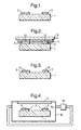
- two metal tracks 2 formed on its upper surface by any conventional technique, such as by deposition through a photo resist mask that is subsequently removed.
- the tracks 2 are about 1-5 ⁇ m thick and may, for example be of nickel, or any other metal effective to produce the catalytic action referred to below, such as silver, copper, titanium, chromium, gold, lanthanum, caesium, magnesium, aluminium or molybdenum.
- a silk screen 3 is placed on the upper surface of the substrate.
- the screen having a pattern of porous regions 13 corresponding to the location of the tracks 2.
- a paste 4 is then wiped over the upper surface of the screen 3 with a squeegee 5 so that the paste is pushed through the porous regions 13 onto the upper surface of the metal tracks 2.
- the paste 4 comprises a low-cost diamond grit, or nanogrit, with a particle size in the range of a few tenths of a micron to a few micron in a binder.
- the screen 3 is then removed and the substrate 1 with its paste-coated tracks 2 is placed in an oven to drive off the binder and leave the diamond grit 6, as shown in Figure 3.
- the density of diamond grit 6 on the tracks 2 is about 10,000 per cm 2 .
- the diamond grit could be deposited by ultrasonic abrasion, to embed it into the upper surface of the metal tracks.
- the pattern of diamond grit could be produced on the surface by any conventional lithography technique, such as using electron-beam or X-ray beam techniques.
- the diamond grit could be coated by a spin-on technique, by printing or by electrophoresis.
- the substrate 1 is placed in a reactor chamber 10.
- the chamber 10 has a 6kW microwave plasma reactor 11 and is connected to a hydrogen gas pump 12.
- the reactor 11 heats the substrate 1 to a temperature in the range 500-1000°C and the pump 12 circulates hydrogen through the chamber 10 at a pressure in the range of a few tenths of a torr to several hundred torr for up to about 1 hour.
- Other forms of hydrogen plasma could be used and the plasma could contain hydrocarbon gases, such as methane.
- Other forms of heating could be used, such as RF heating.
- the metal of the tracks 2 acts as a catalyst in the presence of the hydrogen plasma to cause regrowth of the diamond grit 6 into high quality, faceted, sharp-edged diamond grains of increased size, in the submicron to micron range. It also promotes the interface states formed between the diamond grit and residual metal or carbides, such as carbides formed by reaction between the metal and diamond (this is particularly applicable where the metal is molybdenum or titanium).
- the regrowth of the diamond therefore, leads to an increase in the quality of the diamond because of the increased size and refined shape.
- the adhesion, and hence the electrical contact of the diamond with the underlying surface is also improved.
- the method also has the advantage that the regrowth of the diamond can be achieved relatively quickly.
- the diamond grit 6 may be doped before applying to the tracks, with an n-type or p-type material. Alternatively, the diamond may be doped after applying it to the tracks such as by including the dopant in the hydrogen plasma treatment. This avoids the need for any additional surface treatments or metal coating to enhance electron emission. Diamond grit doped in this way exhibits a desirable depletion layer at the interface between the diamond crystal and the metal layer. Doped diamond grit could be produced by crushing n-type or p-type CVD diamond film. This has been found to enable a ready control of conductivity.
- the metal catalyst could be in powder form mixed with the diamond nanogrit and this powder mixture deposited onto a surface.
- the powder could be a metal oxide or other metal-containing powder.
- the metal layer can be sufficiently thin that it is consumed by the regrowth process. This enables the diamond particle to sink into physical contact with the underlying substrate.
- the completed device may be used in the cathode of a field emission device, such as a display of the kind described in GB2297862.
- the diamond surface could be used in planar emitter arrays, such as in display devices.
- the diamond surface could be applied to a cold cathode electrode such as in an LCD backlight.
- Figures 5 to 8 show a device 20 to 20"' in different arrangements of light-emitting displays.
- the arrangement of Figure 5 is a diode configuration with the device 20 supported on a cathode plate 21 beneath a transparent anode plate 22 having a low voltage phosphor layer 23 on its lower surface.
- the upper, exposed surface of the device 20 faces, and is spaced opposite. the phosphor 23, being separated from it by a vacuum.
- Electrons emitted by the device 20 are attracted to the anode plate 22, by a voltage of between about 500 and 1000volts, and cause the phosphor layer 23 to fluoresce.
- the display would typically incorporate many such devices 20 so that the desired display representation can be produced by appropriately addressing individual devices in a conventional way.
- Figure 6 is similar to that of Figure 5 but is a triode arrangement with a gate plate 24' between the cathode plate 21' and the anode plate 22'. By controlling the voltage on the gate plate 24', the flow of electrons from the device 20' to the anode plate 22' can be controlled.
- the arrangement of Figure 7 has a device 20" operating in a voltage-biased, surface conduction mode.
- Two electrodes 25" and 26" at opposite ends of the device 20" are connected to a low voltage dc source (approximately 14volts), such as a battery 27".
- the arrangement of Figure 8 also has a device 20"' operated in a voltage-biased, surface conduction mode.
- the phosphor 23"' is not located opposite the device 20"' but is mounted on a common insulative plate 28"' with the device, in the same plane.
- the exposed surface of the fluorescent phosphor 23"' therefore, faces in the same direction as that of the device 20"'. Electrons emitted by the device 20"' follow a curved trajectory initially moving away from the plate 28"' and then moving back towards it under the attractive force of the positive voltage on the anode 22"'.
- This configuration has found to have several advantages in electron emitter displays in general compared with conventional configurations where the phosphor is located directly above the electron emitter. In particular.
- the invention could also be used to form diamond surfaces on other devices such as on printed circuit boards where a conventional copper/Invar/copper layer could be replaced with a copper/diamond composite layer.
- the diamond layer has a very high thermal conductivity, making it particularly useful in applications where there is high thermal emission.
- a diamond nanogrit abrasive device formed in this way has an increased effective life compared with conventional diamond grit abrasive devices.
- An abrasive pad formed in this way could be used, for example. in multiple metal layer CMP (chemical metal polishing) planarization processes.
Landscapes
- Chemical & Material Sciences (AREA)
- Engineering & Computer Science (AREA)
- Materials Engineering (AREA)
- Mechanical Engineering (AREA)
- Organic Chemistry (AREA)
- General Chemical & Material Sciences (AREA)
- Chemical Kinetics & Catalysis (AREA)
- Metallurgy (AREA)
- Manufacturing & Machinery (AREA)
- Nanotechnology (AREA)
- Inorganic Chemistry (AREA)
- Mathematical Physics (AREA)
- Crystallography & Structural Chemistry (AREA)
- Theoretical Computer Science (AREA)
- Physics & Mathematics (AREA)
- Crystals, And After-Treatments Of Crystals (AREA)
- Cold Cathode And The Manufacture (AREA)
- Cathode-Ray Tubes And Fluorescent Screens For Display (AREA)
- Control Of Indicators Other Than Cathode Ray Tubes (AREA)
- Chemical Vapour Deposition (AREA)
Applications Claiming Priority (3)
| Application Number | Priority Date | Filing Date | Title |
|---|---|---|---|
| GBGB9626221.7A GB9626221D0 (en) | 1996-12-18 | 1996-12-18 | Diamond surfaces |
| GB9626221 | 1996-12-18 | ||
| EP97949056A EP0946959B1 (de) | 1996-12-18 | 1997-12-12 | Diamantfilmdepositionsmethode |
Related Parent Applications (1)
| Application Number | Title | Priority Date | Filing Date |
|---|---|---|---|
| EP97949056A Division EP0946959B1 (de) | 1996-12-18 | 1997-12-12 | Diamantfilmdepositionsmethode |
Publications (2)
| Publication Number | Publication Date |
|---|---|
| EP0962957A2 true EP0962957A2 (de) | 1999-12-08 |
| EP0962957A3 EP0962957A3 (de) | 2000-02-02 |
Family
ID=10804599
Family Applications (2)
| Application Number | Title | Priority Date | Filing Date |
|---|---|---|---|
| EP97949056A Expired - Lifetime EP0946959B1 (de) | 1996-12-18 | 1997-12-12 | Diamantfilmdepositionsmethode |
| EP99304377A Withdrawn EP0962957A3 (de) | 1996-12-18 | 1997-12-12 | Lichtemittierende Anzeigevorrichtungen |
Family Applications Before (1)
| Application Number | Title | Priority Date | Filing Date |
|---|---|---|---|
| EP97949056A Expired - Lifetime EP0946959B1 (de) | 1996-12-18 | 1997-12-12 | Diamantfilmdepositionsmethode |
Country Status (8)
| Country | Link |
|---|---|
| US (1) | US6284556B1 (de) |
| EP (2) | EP0946959B1 (de) |
| JP (2) | JP4176838B2 (de) |
| KR (1) | KR100372597B1 (de) |
| AU (1) | AU7740098A (de) |
| DE (1) | DE69719214T2 (de) |
| GB (1) | GB9626221D0 (de) |
| WO (1) | WO1998027568A1 (de) |
Families Citing this family (31)
| Publication number | Priority date | Publication date | Assignee | Title |
|---|---|---|---|---|
| US9238207B2 (en) | 1997-04-04 | 2016-01-19 | Chien-Min Sung | Brazed diamond tools and methods for making the same |
| US9199357B2 (en) | 1997-04-04 | 2015-12-01 | Chien-Min Sung | Brazed diamond tools and methods for making the same |
| US9868100B2 (en) | 1997-04-04 | 2018-01-16 | Chien-Min Sung | Brazed diamond tools and methods for making the same |
| US9221154B2 (en) | 1997-04-04 | 2015-12-29 | Chien-Min Sung | Diamond tools and methods for making the same |
| US9463552B2 (en) | 1997-04-04 | 2016-10-11 | Chien-Min Sung | Superbrasvie tools containing uniformly leveled superabrasive particles and associated methods |
| US9409280B2 (en) | 1997-04-04 | 2016-08-09 | Chien-Min Sung | Brazed diamond tools and methods for making the same |
| DE19757141A1 (de) * | 1997-12-20 | 1999-06-24 | Philips Patentverwaltung | Array aus Diamant/wasserstoffhaltigen Elektroden |
| GB2350925A (en) * | 1999-03-06 | 2000-12-13 | Smiths Industries Plc | Making an electron-emitter by ink-jet printing |
| US6350680B1 (en) | 2000-05-26 | 2002-02-26 | Taiwan Semiconductor Manufacturing Company | Pad alignment for AlCu pad for copper process |
| KR20010113402A (ko) * | 2000-06-19 | 2001-12-28 | 김대옥 | 합성보석의 파빌리온면 표면처리방법 및 표면코팅구조 |
| US6727117B1 (en) * | 2002-11-07 | 2004-04-27 | Kyocera America, Inc. | Semiconductor substrate having copper/diamond composite material and method of making same |
| US20070267291A1 (en) * | 2004-03-09 | 2007-11-22 | Hall Clive E | Electrochemical Sensor Comprising Diamond Particles |
| US7384436B2 (en) * | 2004-08-24 | 2008-06-10 | Chien-Min Sung | Polycrystalline grits and associated methods |
| US9138862B2 (en) | 2011-05-23 | 2015-09-22 | Chien-Min Sung | CMP pad dresser having leveled tips and associated methods |
| US8678878B2 (en) | 2009-09-29 | 2014-03-25 | Chien-Min Sung | System for evaluating and/or improving performance of a CMP pad dresser |
| US8622787B2 (en) | 2006-11-16 | 2014-01-07 | Chien-Min Sung | CMP pad dressers with hybridized abrasive surface and related methods |
| US8393934B2 (en) | 2006-11-16 | 2013-03-12 | Chien-Min Sung | CMP pad dressers with hybridized abrasive surface and related methods |
| US9724802B2 (en) | 2005-05-16 | 2017-08-08 | Chien-Min Sung | CMP pad dressers having leveled tips and associated methods |
| US8398466B2 (en) | 2006-11-16 | 2013-03-19 | Chien-Min Sung | CMP pad conditioners with mosaic abrasive segments and associated methods |
| CN100444697C (zh) * | 2006-06-07 | 2008-12-17 | 东南大学 | 平面式场发射三极结构及其制备方法 |
| JP2009099367A (ja) * | 2007-10-16 | 2009-05-07 | Fuji Heavy Ind Ltd | 発光装置 |
| CN101903131B (zh) | 2007-11-13 | 2013-01-02 | 宋健民 | Cmp垫修整器 |
| JP4303308B2 (ja) * | 2007-11-20 | 2009-07-29 | シャープ株式会社 | 電子放出素子、電子放出装置、自発光デバイス、画像表示装置、送風装置、冷却装置、帯電装置、画像形成装置、電子線硬化装置、および電子放出素子の製造方法 |
| TWI388402B (en) | 2007-12-06 | 2013-03-11 | Methods for orienting superabrasive particles on a surface and associated tools | |
| CN101540260B (zh) * | 2008-03-19 | 2011-12-14 | 清华大学 | 场发射显示器 |
| US20100139885A1 (en) * | 2008-12-09 | 2010-06-10 | Renewable Thermodynamics, Llc | Sintered diamond heat exchanger apparatus |
| US8299700B2 (en) | 2009-02-05 | 2012-10-30 | Sharp Kabushiki Kaisha | Electron emitting element having an electron acceleration layer, electron emitting device, light emitting device, image display device, cooling device, and charging device |
| JP4732533B2 (ja) | 2009-05-19 | 2011-07-27 | シャープ株式会社 | 電子放出素子及びその製造方法、並びに、電子放出装置、帯電装置、画像形成装置、電子線硬化装置、自発光デバイス、画像表示装置、送風装置、冷却装置 |
| JP4880740B2 (ja) | 2009-12-01 | 2012-02-22 | シャープ株式会社 | 電子放出素子及びその製造方法、並びに、電子放出装置、帯電装置、画像形成装置、電子線硬化装置、自発光デバイス、画像表示装置、送風装置、冷却装置 |
| CN103221180A (zh) | 2010-09-21 | 2013-07-24 | 铼钻科技股份有限公司 | 具有基本平坦颗粒尖端的超研磨工具及其相关方法 |
| WO2012162430A2 (en) | 2011-05-23 | 2012-11-29 | Chien-Min Sung | Cmp pad dresser having leveled tips and associated methods |
Family Cites Families (9)
| Publication number | Priority date | Publication date | Assignee | Title |
|---|---|---|---|---|
| ATE193156T1 (de) * | 1990-12-28 | 2000-06-15 | Canon Kk | Bilderzeugungsgerät |
| DE69229485T2 (de) * | 1991-02-01 | 1999-10-21 | Fujitsu Ltd., Kawasaki | Anordnung für Feldemissions-Mikrokathoden |
| US5345141A (en) | 1993-03-29 | 1994-09-06 | Motorola, Inc. | Single substrate, vacuum fluorescent display |
| US5340997A (en) * | 1993-09-20 | 1994-08-23 | Hewlett-Packard Company | Electrostatically shielded field emission microelectronic device |
| US5504385A (en) * | 1994-08-31 | 1996-04-02 | At&T Corp. | Spaced-gate emission device and method for making same |
| US5637950A (en) * | 1994-10-31 | 1997-06-10 | Lucent Technologies Inc. | Field emission devices employing enhanced diamond field emitters |
| US5709577A (en) * | 1994-12-22 | 1998-01-20 | Lucent Technologies Inc. | Method of making field emission devices employing ultra-fine diamond particle emitters |
| US5616368A (en) * | 1995-01-31 | 1997-04-01 | Lucent Technologies Inc. | Field emission devices employing activated diamond particle emitters and methods for making same |
| US5648699A (en) * | 1995-11-09 | 1997-07-15 | Lucent Technologies Inc. | Field emission devices employing improved emitters on metal foil and methods for making such devices |
-
1996
- 1996-12-18 GB GBGB9626221.7A patent/GB9626221D0/en active Pending
-
1997
- 1997-12-12 WO PCT/GB1997/003445 patent/WO1998027568A1/en not_active Ceased
- 1997-12-12 AU AU77400/98A patent/AU7740098A/en not_active Abandoned
- 1997-12-12 DE DE69719214T patent/DE69719214T2/de not_active Expired - Lifetime
- 1997-12-12 KR KR10-1999-7005165A patent/KR100372597B1/ko not_active Expired - Fee Related
- 1997-12-12 EP EP97949056A patent/EP0946959B1/de not_active Expired - Lifetime
- 1997-12-12 EP EP99304377A patent/EP0962957A3/de not_active Withdrawn
- 1997-12-12 US US09/308,271 patent/US6284556B1/en not_active Expired - Lifetime
- 1997-12-12 JP JP52745098A patent/JP4176838B2/ja not_active Expired - Fee Related
-
1999
- 1999-08-16 JP JP22982699A patent/JP2001101985A/ja active Pending
Also Published As
| Publication number | Publication date |
|---|---|
| DE69719214T2 (de) | 2003-07-24 |
| GB9626221D0 (en) | 1997-02-05 |
| WO1998027568A1 (en) | 1998-06-25 |
| JP4176838B2 (ja) | 2008-11-05 |
| US6284556B1 (en) | 2001-09-04 |
| EP0946959B1 (de) | 2003-02-19 |
| JP2001101985A (ja) | 2001-04-13 |
| EP0946959A1 (de) | 1999-10-06 |
| KR100372597B1 (ko) | 2003-02-17 |
| KR20000057490A (ko) | 2000-09-15 |
| AU7740098A (en) | 1998-07-15 |
| DE69719214D1 (en) | 2003-03-27 |
| JP2001506959A (ja) | 2001-05-29 |
| EP0962957A3 (de) | 2000-02-02 |
Similar Documents
| Publication | Publication Date | Title |
|---|---|---|
| EP0962957A2 (de) | Lichtemittierende Anzeigevorrichtungen | |
| EP0709870B1 (de) | Verfahren und Vorrichtung zur Herstellung von teilchenförmigen und verbesserten Feldemittern und so erhaltene Produkte | |
| US6626724B2 (en) | Method of manufacturing electron emitter and associated display | |
| US6462467B1 (en) | Method for depositing a resistive material in a field emission cathode | |
| US5982095A (en) | Plasma displays having electrodes of low-electron affinity materials | |
| EP1111647A2 (de) | Elektronenemissionsvorrichtung, Kaltkathoden-Feldemissionsvorrichtung und Verfahren zu deren Herstellung, Anzeigevorrichtung mit Kaltkathodenfeldemitter und Verfahren zu deren Herstellung | |
| US6645402B1 (en) | Electron emitting device, electron emitting source, image display, and method for producing them | |
| US7741764B1 (en) | DLC emitter devices and associated methods | |
| US6538368B1 (en) | Electron-emitting devices | |
| JP3737688B2 (ja) | 電子放出素子及びその製造方法 | |
| US7358658B2 (en) | Amorphous diamond materials and associated methods for the use and manufacture thereof | |
| US20060017368A1 (en) | Transparent light-emitting conductive layer and electron emission device including transparent light-emitting conductive layer | |
| WO1998045868A1 (en) | Electron emitting device and method of manufacturing the same | |
| US6777169B2 (en) | Method of forming emitter tips for use in a field emission display | |
| JPH09185942A (ja) | 冷陰極素子及びその製造方法 | |
| JP3724145B2 (ja) | 電子放出素子およびその製造方法、および画像表示装置およびその製造方法 | |
| US6504311B1 (en) | Cold-cathode cathodoluminescent lamp | |
| JP3387005B2 (ja) | 電子放出素子及びその製造方法 | |
| KR20010104960A (ko) | 전계방출소자용 캐소드 및 그 제조방법 | |
| KR100357348B1 (ko) | 전계방출표시소자 및 그 제조방법 | |
| KR100450025B1 (ko) | 탄소나노튜브를 이용한 3극구조를 가지는 평판형전계방출램프 및 그 제조방법 | |
| JPH11265654A (ja) | ダイヤモンド/水素を含む電極アレー | |
| JP2004031090A (ja) | 電子放出素子 | |
| JP2002289089A (ja) | 電界放射冷陰極及びその製造方法 | |
| GB2350925A (en) | Making an electron-emitter by ink-jet printing |
Legal Events
| Date | Code | Title | Description |
|---|---|---|---|
| PUAI | Public reference made under article 153(3) epc to a published international application that has entered the european phase |
Free format text: ORIGINAL CODE: 0009012 |
|
| AC | Divisional application: reference to earlier application |
Ref document number: 946959 Country of ref document: EP |
|
| AK | Designated contracting states |
Kind code of ref document: A2 Designated state(s): DE FR GB |
|
| PUAL | Search report despatched |
Free format text: ORIGINAL CODE: 0009013 |
|
| AK | Designated contracting states |
Kind code of ref document: A3 Designated state(s): DE FR GB |
|
| 17P | Request for examination filed |
Effective date: 20000524 |
|
| STAA | Information on the status of an ep patent application or granted ep patent |
Free format text: STATUS: THE APPLICATION IS DEEMED TO BE WITHDRAWN |
|
| 18D | Application deemed to be withdrawn |
Effective date: 20020703 |