EP0963036A2 - Circuit amplificateur de puissance et procédé de commande automatique de puissance - Google Patents
Circuit amplificateur de puissance et procédé de commande automatique de puissance Download PDFInfo
- Publication number
- EP0963036A2 EP0963036A2 EP99110637A EP99110637A EP0963036A2 EP 0963036 A2 EP0963036 A2 EP 0963036A2 EP 99110637 A EP99110637 A EP 99110637A EP 99110637 A EP99110637 A EP 99110637A EP 0963036 A2 EP0963036 A2 EP 0963036A2
- Authority
- EP
- European Patent Office
- Prior art keywords
- efficiency
- control
- amplifier
- power
- value
- Prior art date
- Legal status (The legal status is an assumption and is not a legal conclusion. Google has not performed a legal analysis and makes no representation as to the accuracy of the status listed.)
- Withdrawn
Links
Images


Classifications
-
- H—ELECTRICITY
- H03—ELECTRONIC CIRCUITRY
- H03F—AMPLIFIERS
- H03F1/00—Details of amplifiers with only discharge tubes, only semiconductor devices or only unspecified devices as amplifying elements
- H03F1/02—Modifications of amplifiers to raise the efficiency, e.g. gliding Class A stages, use of an auxiliary oscillation
- H03F1/0205—Modifications of amplifiers to raise the efficiency, e.g. gliding Class A stages, use of an auxiliary oscillation in transistor amplifiers
- H03F1/0261—Modifications of amplifiers to raise the efficiency, e.g. gliding Class A stages, use of an auxiliary oscillation in transistor amplifiers with control of the polarisation voltage or current, e.g. gliding Class A
-
- H—ELECTRICITY
- H03—ELECTRONIC CIRCUITRY
- H03F—AMPLIFIERS
- H03F1/00—Details of amplifiers with only discharge tubes, only semiconductor devices or only unspecified devices as amplifying elements
- H03F1/02—Modifications of amplifiers to raise the efficiency, e.g. gliding Class A stages, use of an auxiliary oscillation
- H03F1/0205—Modifications of amplifiers to raise the efficiency, e.g. gliding Class A stages, use of an auxiliary oscillation in transistor amplifiers
- H03F1/0211—Modifications of amplifiers to raise the efficiency, e.g. gliding Class A stages, use of an auxiliary oscillation in transistor amplifiers with control of the supply voltage or current
-
- H—ELECTRICITY
- H03—ELECTRONIC CIRCUITRY
- H03G—CONTROL OF AMPLIFICATION
- H03G3/00—Gain control in amplifiers or frequency changers
- H03G3/20—Automatic control
- H03G3/30—Automatic control in amplifiers having semiconductor devices
- H03G3/3036—Automatic control in amplifiers having semiconductor devices in high-frequency amplifiers or in frequency-changers
- H03G3/3042—Automatic control in amplifiers having semiconductor devices in high-frequency amplifiers or in frequency-changers in modulators, frequency-changers, transmitters or power amplifiers
Definitions
- the present invention relates to a power amplifying circuit having an automatic power control function for use in radio transmitters and the like.
- a portable radio apparatus for instance, is controlled to raise its transmission power when the level of signals received from it at the base station is not high enough. Or if the level of signals received from a portable radio apparatus is unnecessarily high at the base station, control is effected to reduce the transmission power of that portable unit. Therefore, radio transmitters are provided with an automatic power control (APC) function to match the transmission power of each to an individually set level.
- APC automatic power control
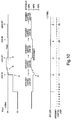
- Fig. 15 is a block diagram illustrating a power amplifying circuit with an APC function according to the prior art, described in the Gazette of the Japanese Utility Model Laid-open No. Hei 3-9522.
- a preamplifier 41 and an amplifier 42 consisting of field effect transistors (FETs) amplify input signals inputted to an input terminal 1.
- FETs field effect transistors
- the level of output power is detected by a detecting circuit 4.
- the output power level detected by the detecting circuit 4 and a set output power level inputted to a set input terminal 10 are inputted to an APC circuit 9.
- the drain voltage of the preamplifier 41 and the amplifier 42 is determined to make the output power level identical with the set output power level, and this voltage is applied to the drain terminals of the preamplifier 41 and the amplifier 42.
- the set output power level and the drain voltage determined by the APC circuit 9 are inputted to an idle current control circuit 43, which determines the idle current during the absence of radio signals so as to maximize the power efficiency on the basis of the set output power level and drain voltage at the time, and applies a voltage matching the idle current to the gates of the preamplifier 41 and the amplifier 42.
- the idle current control circuit 43 controls the gate bias of the preamplifier 41 and the amplifier 42 so as to enhance the power efficiency.
- the power amplifying circuit referred to above controls the idle current according to the set output power level of each unit, but does not actually measure or calculate the efficiency and performs control on that basis.
- it is an open loop control arrangement to determine the gate bias according to the control output of the APC function.
- the gate bias value is determined indiscriminately according to the set output power level of each.
- the gate bias value to give the maximum efficiency may vary with the input power level, temperature and frequency among other factors. Therefore the above-cited power amplifying circuit involves the problem that the gate bias value to provide the maximum efficiency may deviate from the optimal value.
- the performance characteristics of an amplifiers (including the input/output characteristic, temperature characteristic, frequency characteristic, output power versus drain voltage characteristic, efficiency versus gate current characteristic and static characteristic) generally tend to fluctuate.
- the input/output characteristic, temperature characteristic, frequency characteristic, output power versus drain voltage characteristic, efficiency versus gate current characteristic and static characteristic generally tend to fluctuate.
- an object of the present invention is to provide a power amplifying circuit having an APC function which can provide a high power efficiency all the time even if such conditions of operation as the output power level, input power level, temperature and frequency vary, and can automatically keep the power efficiency high even if amplifier characteristics are not constant.
- a power amplifying circuit is provided with an APC loop for causing the output power level to comply with the set output power level and an efficiency control loop for detecting the power efficiency (output power/power consumption) and controlling the bias value of an amplifier arranged in the power amplifying circuit so as to maximize the power efficiency.
- the efficiency control loop may have a configuration comprising an arithmetic means for calculating the power efficiency of the power amplifying circuit by introducing the input current, the input voltage and the output power level of the power amplifying circuit, and a bias control means for controlling the bias value of the amplifier on the basis of an efficiency value outputted from the arithmetic means.
- the arithmetic means intended to calculate the efficiency value at prescribed intervals of time
- the bias control means may have a configuration wherein the efficiency value currently outputted from the arithmetic means and the efficiency value outputted from the arithmetic means at the preceding control timing are compared, and the bias value of the amplifier is altered if the two efficiency values are not identical.
- the bias control means may have a configuration wherein, if the efficiency value currently outputted from the arithmetic means is greater than the preceding efficiency value, the bias value is varied in the same direction in which it was varied at the preceding control timing, or if the efficiency value currently outputted from the arithmetic means is smaller than the preceding efficiency value, the bias value is varied in the direction reverse to that in which it was varied at the preceding control timing.
- the amplifier is a FET, and the configuration may be such that the APC loop controls the drain bias value of the FET and the efficiency control loop controls the gate bias value of the FET.
- the response of the APC loop should be quicker than that of the efficiency control loop.
- the efficiency control loop may have a configuration wherein control is effected when the output power level of the amplifier is identical with the set output power level.
- the power amplifying circuit may have a configuration wherein a presetting means stores control setpoints to give the maximum efficiency at different set output power levels and, when the set output power level changes, outputs a control setpoint matching the changed level to the amplifier.
- the power amplifying circuit may have a configuration wherein an input level detecting means for detecting the input power level of the amplifier is provided, and the presetting means has control setpoints to give the maximum efficiency at different input power levels and, when the input power level changes, outputs a control setpoint matching the changed level to the amplifier.
- the power amplifying circuit may have a configuration wherein a temperature detecting means for detecting the temperature is provided, and the presetting means stores bias value to give the maximum efficiency at different temperatures and, when the temperature changes, outputs a control setpoint matching the changed temperature to the amplifier.
- the presetting means may as well have a configuration to store control setpoints to give the maximum efficiency at different frequencies and, when the frequency of signals inputted to the amplifier changes, to output a control setpoint matching the changed frequency to the amplifier.
- a power amplifying circuit having any of the foregoing configurations may amplify constant-envelope-modulated signals.
- An automatic power control method is so composed as to detect the output power level of a power amplifying circuit, to control an amplifier provided in the power amplifying circuit so as to make the detected output power level identical with a set output power level, to measure the power efficiency of the power amplifying circuit, and to control the bias value of the amplifier so as to maximize the power efficiency.
- the automatic power control method may as well have a composition wherein the power efficiency of an amplifier is measured intermittently, each measured efficiency value is compared with the efficiency value measured at the preceding measurement timing and, if the two efficiency values are not identical, the bias value of the amplifier is varied in the direction of enhancing the power efficiency.
- composition may as well be such that, if the currently measured efficiency value is greater than the preceding efficiency value, the bias value is varied in the same direction in which it was varied at the preceding measurement timing, or if the currently measured efficiency value is smaller than the preceding efficiency value, the bias value is varied in the direction reverse to that in which it was varied at the preceding measurement timing.
- constant envelope-modulated signals may be the objects of power control.
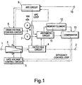
- Fig. 1 is a block diagram illustrating a power amplifying circuit which is a first embodiment of the present invention.
- an amplifier 3 consisting of a MOSFET amplifies input signals inputted to an input terminal 1. Whereas output signals from the amplifier 3 are outputted from an output terminal 2, the output power level is detected by a detecting circuit 4.
- To an APC circuit 9 are inputted the output power level detected by the detecting circuit 4 and a set output power level inputted to a set input terminal 10.
- the drain voltage of the amplifier 3 is determined so as to make the output power level identical with the set output power level, and a control command value is outputted to a drain voltage control circuit 6, which applies a voltage matching the control command value to the drain terminal of the amplifier 3.
- Fig. 2 is a circuit diagram illustrating one example of the configuration of the amplifier 3 and the drain voltage control circuit 6.
- the amplifier 3 uses a FET 31 which introduces input signals to the gate via a capacitor Cin.
- a gate bias voltage which is controlled by a gate voltage control circuit 5.
- a drain bias voltage which is controlled by the drain voltage control circuit 6.
- the output of the FET 31 is taken out via the resistor RD and a capacitor Cout.
- a source voltage Vdd controlled by an N-ch MOSFET 61 is applied to the drain of the amplifier 3.
- To the gate of the MOSFET 61 is applied via an operational amplifier 62 a voltage matching the control command value determined by the APC circuit 9.
- an ammeter 8 and a voltmeter 7 Between the drain voltage control circuit 6 and the power source are provided an ammeter 8 and a voltmeter 7. To an arithmetic circuit 11 are inputted the amperage from the ammeter 8, the voltage from the voltmeter 7 and the output power level detected by the detecting circuit 4. On their basis, the arithmetic circuit 11 calculates the power efficiency, and outputs the calculated efficiency value to a memory element 12 and a comparator 13.
- the comparator 13 compares the efficiency value of a round before written in the memory element 12 and the current efficiency value delivered from the arithmetic circuit 11, and determines the gate voltage on the basis of the result of comparison so as to maximize the power efficiency, and outputs the determined value to the gate voltage control circuit 5 as the control command value.
- the gate voltage control circuit 5 applies to the gate terminal of the amplifier 3 a voltage matching the control command value.
- a "round” in this context means an interval of intermittent control over the gate voltage of the amplifier 3.
- the output power level is kept at the set output power level because the drain voltage of the amplifier 3 is controlled by the APC circuit 9.
- the arithmetic means is realized by the arithmetic circuit 11, and the bias control means, by the comparator 13 and the gate voltage control circuit 5.
- the APC circuit 9, the arithmetic circuit 11, the memory element 12 and the comparator 13 can be realized, for instance, by a single microprocessor. In that case, processing by the APC loop and that by the efficiency control loop are realized by software.
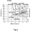
- Fig. 3 is a diagram for explaining the dependence of the power efficiency and the gate voltage on the drain voltage when the input power level, temperature and frequency are kept constant, with the output power level of the amplifier 3 consisting of a MOSFET being used as the parameter.
- the combination of drain voltage and gate voltage that gives the maximum efficiency is that of the two voltages at point a .
- the combination of drain voltage and gate voltage that gives the maximum efficiency is that of the two voltages at point b .
- the drain current will have to be increased by raising the gate voltage to achieve the prescribed output power level.
- the operating class of the amplifier 3 will come closer to "A" and its power efficiency will drop.
- the saturation output power of the amplifier 3 will also rise, resulting in an enlarged difference between the saturation output power and the prescribed output power level.
- an increase output back-off will invite a drop in efficiency.
- a tradeoff between the operating class and the output back-off determines only one combination of drain voltage and gate voltage that gives the maximum efficiency.
- the power amplifying circuit of this embodiment includes an APC loop and an efficiency control loop.
- Fig. 4 is a flow chart showing the operation of the APC loop.
- the APC loop as indicated by broken lines in Fig. 1, comprises the amplifier 3, the detecting circuit 4, the APC circuit 9 and the drain voltage control circuit 6.
- one round of the APC loop is accomplished in 1 ms.
- the APC circuit 9 effects control over the drain voltage control circuit 6 every millisecond.
- the detecting circuit 4 obtains the output power of the amplifier 3 on the basis of the detection voltage (step S1). For instance, the detecting circuit 4, having a table of detection voltage versus output power, obtains the output power by searching the table on the basis of the detection voltage, and actuates a 1 ms timer (step S2).
- the drain voltage control circuit 6 raises, reduces or maintains the gate voltage of the amplifier 3 according to the control command value from the APC circuit 9 (step S7). After that, when the timer has completed counting 1 ms (step S8), a counter is counted up by +1 (step S9). This counter is used for determining the control timing of the efficiency control loop.
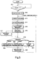
- Fig. 5 is a flow chart showing the operation off the efficiency control loop.
- the efficiency control loop as indicated by broken lines in Fig. 1, comprises the amplifier 3, the arithmetic circuit 11, the memory element 12, the comparator 13 and the gate voltage control circuit 5.
- the efficiency control loop operates in parallel with the APC loop.
- the response speed of the efficiency control loop is set to be 1/7 of that of the APC loop. Therefore, when the count of the aforementioned counter comes to 7, the arithmetic circuit 11 calculates the power efficiency, and the comparator 13 controls the gate voltage control circuit 5.
- the arithmetic circuit 11 waits until the counter counts 7 (step S22), and initializes the counter when its count comes to 7 (step 12).
- the counter is counted up under the control of the APC loop as stated above.
- To the arithmetic circuit 11 are inputted the amperage detected by the ammeter 8, the voltage detected by the voltmeter 7, and the output power level detected by the detecting circuit 4 (steps S13 to S15). It calculates the input power from the detected voltage and amperage, and also calculates the power efficiency of the amplifier 3 from the input power and output power level (step S16).
- the arithmetic circuit 11 outputs the calculated efficiency value to the comparator 13 and stores it into the memory element 12 (step S17).
- the power efficiency here also reflects power consumption by the drain voltage control circuit 6 and the gate voltage control circuit 5.
- the comparator 13 compares the inputted efficiency value and the efficiency value stored into the memory element 12 one round before (step S18).
- the comparator 13 controls the gate voltage control circuit 5 in the direction reverse to that in which it effected control in the preceding round (step S20). If the current efficiency value is equal to the efficiency value of the round before, the comparator 13 controls the gate voltage control circuit 5 to maintain the gate voltage of the round before (step S21).
- the gate voltage control circuit 5 raises, reduces or maintains the gate voltage of the amplifier 3 according to the control command value from the comparator 13 (step S22).
- the efficiency control loop might reduce the gate voltage to its lower limit before the output power level is controlled, making it impossible for the output power level to be controlled, It is for this reason that the response of the efficiency control loop is set to be slower than that of the APC loop.
- the response speed of the APC loop is set to be seven times as high as that of the efficiency control loop, Whereas the response speed of the efficiency control loop is set to be about 5 ms when the data transfer speed is 5.6 kbps for instance, this can be readily realized by appropriately changing the setpoint of the aforementioned timer.
- the ratio between the response speed of the APC loop and that of the efficiency control loop can also be readily changed by varying the criterion count of the counter (7 in this instance).
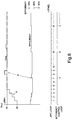
- Fig. 6 is a timing chart showing how a bias point which gives the maximum efficiency is converged upon by above-described control,
- the set output power value changes from 32 dBm to 34 dBm, and the response speed of the APC loop is seven times as high as that of the efficiency control loop.
- FIG. 7 is a diagram for explaining the operation that takes place when the set output voltage level has varied from 32 dBm to 34 dBm. In this illustration, the control steps of the gate voltage are shown bigger than the steps in practical use. Further to facilitate description, the comparator 13 is supposed to be able to detected even infinitesimal differences, and the response speed of the APC loop, to be sufficiently higher than that of the efficiency control loop.
- the bias point is set at point 101, where the maximum efficiency is achieved. Further, it is supposed that the bias point which gives the maximum efficiency when the output power level is 34 dBm is point 106. As the set output power level varies to 34 dBm, the drain voltage rises under the control of the APC loop, and the bias point shifts to point 102.
- the arithmetic circuit 11 in the efficiency control loop calculates the efficiency value under the bias condition at point 102, and outputs the efficiency value to the memory element 12 and the comparator 13.
- the comparator 13 compares the efficiency value under the bias condition at point 102 and the efficiency value of one round before, stored in the memory element 12. As the current efficiency value here differs from the efficiency value of one round before, the comparator 13 instructs the gate voltage control circuit 5 to alter the gate voltage. Accordingly, the bias point shifts to point 103 or point 111.
- the comparator 13 instructs the gate voltage control circuit 5 to effect control in the reverse direction, i.e. to lower the gate voltage. Then the bias point shifts to point 111. If the current efficiency value is lower than that of one round before and control was effected at the timing of one round before to lower the gate voltage, the comparator 13 instructs the gate voltage control circuit 5 to effect control in the reverse direction, i.e. to raise the gate voltage, Then the bias point shifts to point 103. In short, the bias point shifts to either point 103 or point 111 depending on the then prevailing conditions (the input power level, output power level, temperature, frequency, characteristic of the amplifier 3, and variation of the output power level).
- the comparator 13 effects control either to raise or to lower the gate voltage.
- the bias point shifts to point 103 (the control is in the direction of raising the gate voltage)
- the bias point immediately shifts to point 104 under the control of the APC loop.
- the arithmetic circuit 11 in the efficiency control loop calculates the efficiency value under the bias condition at point 104, and outputs the efficiency value to the memory element 12 and the comparator 13.
- the comparator 13 instructs the gate voltage control circuit 5 to control the gate voltage in the same direction as before. Since the control was in the direction of raising the gate voltage in the preceding round, the gate voltage control circuit 5 raises the gate voltage. Accordingly, the bias point shifts to point 105. Then the bias point immediately shifts to point 106 under the control of the APC loop.
- the arithmetic circuit 11 in the efficiency control loop then calculates the efficiency value under the bias condition at point 106, and outputs the efficiency value to the memory element 12 and the comparator 13.
- the comparator 13 instructs the gate voltage control circuit 5 to control the gate voltage in the same direction as before. Since the control was in the direction of raising the gate voltage in the preceding round, the gate voltage control circuit 5 raises the gate voltage. Accordingly, the bias point shifts to point 107, but the bias point immediately shifts to point 108 under the control of the APC loop.
- the gate voltage is controlled this time in the reverse direction, and therefore the bias point shifts to point 109. However, the bias point immediately shifts to point 106 under the control of the APC loop.
- the gate voltage is controlled in the same direction, and the bias point shifts to point 110, but the bias point immediately shifts to point 104 under the control of the APC loop.
- bias point repeats shifting to points 104, 105, 106, 107, 108, 109, 106, 110 and 104, and substantially converges on point 106, which is the bias point giving the maximum efficiency.
- the bias point shifts to point 110 (the control is in the direction of lowering the gate voltage) when the set output power level has been altered to 34 dBm, the bias point immediately shifts to point 112 under the control of the APC loop.
- the gate voltage is controlled in the direction reverse to the preceding round (in the direction of raising the gate voltage in this instance), and the bias point shifts to point 113, but the bias point immediately shifts to point 102 under the control of the APC loop.
- the gate voltage is controlled in the same direction as in the preceding round, and the bias point shifts to point 103, but the bias point immediately shifts to point 104 under the control of the APC loop.
- the bias point repeats shifting to points 104, 105, 106, 107, 108, 109, 106, 110 and 104, and substantially converges on the bias point giving the maximum efficiency.
- the efficiency will greatly vary in a step, but the comparator 13 may be unable to detect the difference and judge that the efficiency has not varied. If it does, the convergence may deviate from the bias point which should provide the maximum efficiency. Or if the control steps of the gate voltage are too small and if the criterion of judgment by the comparator 13 is relatively loose, the efficiency will hardly vary in a step, and the comparator 13 may be unable to detect the difference and judge that convergence has taken place before the bias point which should provide the maximum efficiency is reached.
- the size of control steps of the gate voltage and the resolution of the comparator 13 are set so as to make it impossible to detect any difference in efficiency between point 106 and the adjoining points 104 and 108.
- the control step size is set to be a few millivolts and the resolution of efficiency by the comparator 13, about ⁇ 0.05%.
- the comparator 13 in the efficiency control loop detects any drop in power efficiency, and automatically instructs the gate voltage control circuit 5 so as to set the gate voltage which gives the maximum efficiency.
- the efficiency control loop will automatically function to cause bias points to converge the point where the maximum efficiency is achieved.
- Fig. 8 is a timing chart showing an example for comparison of the operation of the efficiency control loop,
- the response speed of the efficiency control loop is higher than that of the APC loop.
- the set output power value is altered from 32 dBm to 34 dBm, as the APC loop does not work at first, the efficiency control loop maintains the maximum efficiency at 32 dBm (see A in Fig. 8).
- the APC loop begins to work, the output power level of the amplifier 3 rises and, along with that, the efficiency drops (see B in Fig. 8).
- Fig. 9 is a block diagram illustrating a power amplifying circuit which is a second embodiment of the present invention. As shown in Fig. 9, in this embodiment, the APC circuit 9 and the arithmetic circuit 11 are connected by a setting level identity signal line 14. While other aspects of the configuration are the same as the corresponding ones of the first embodiment, the arithmetic circuit 11 in this embodiment either operates or interrupts operation depending on the signal emerging on the setting level identity signal line 14.
- the APC loop performs control similar to that in the first embodiment, and makes the output power level of the amplifier 3 identical with the set output power level, Then the APC circuit 9 outputs an ON signal via the setting level identity signal line 14 if the output power level is identical with the set output power level as controlled by the APC loop. If the output power level is not identical with the set output power level, the APC circuit 9 outputs an OFF signal.
- the arithmetic circuit 11 calculates the power efficiency from the drain amperage, drain voltage and power output level of the amplifier 3 only when an ON signal is on the setting level identify signal line 14, and outputs the calculated efficiency value to the memory element 12 and the comparator 13.
- the comparator 13 and the gate voltage control circuit 5, operating in the same manner as in the first embodiment, provides a gate voltage that gives the maximum efficiency to the gate terminal of the amplifier 3.
- the arithmetic circuit 11 When an OFF signal is on the setting level identify signal line 14, the arithmetic circuit 11 does not calculate the power efficiency. As no updated efficiency value is inputted to the comparator 13, the comparator 13 continues to control the gate voltage control circuit 5 so as to keep the gate voltage of the amplifier 3 as it is. Thus, when an OFF signal is on the setting level identify signal line 14, no control by the efficiency control loop takes place.
- the efficiency control loop operates only when the APC loop is converging on the set output power level. Therefore, if has the advantage of permitting the response speed of the APC loop and that of the efficiency control loop to be set separately and as desired.
- Fig. 10 is a timing chart showing an example of how a bias point which gives the maximum efficiency is converged upon in this embodiment,
- the set output power level varies from 32 dBm to 34 dBm, and the response speed of the APC loop is lower than that of the efficiency control loop.
- the APC loop operates to change the output power level of the amplifier 3 to 34 dBm.
- the efficiency drops along with that.
- the efficiency control loop begins to work (see A of Fig. 10).
- the efficiency control loop serves to enhance the efficiency.
- the output power level deviates from 34 dBm along with that (see B of Fig. 10).
- the output power level returns to 34 dBm (see C of Fig. 10). After that, efficiency enhancement by the efficiency control loop and output power control by the APC loop are repeated to settle the output of the amplifier 3 at 34 dBm, where the maximum efficiency is achieved.
- the output power level of the amplifier 3 can be brought back to the set level. Therefore, even if the gate voltage is reduced by the efficiency control loop, the output power level is brought back toward the set level the moment the APC loop begins to work.
- the response speed of the APC loop and that of the efficiency control loop can be set separately and as desired, and moreover the response speed of the APC loop may be lower than that of the efficiency control loop.
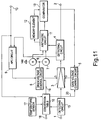
- Fig. 11 is a block diagram illustrating a power amplifying circuit which is a third embodiment of the present invention.
- a detecting circuit 15 for input power level detection is inserted on the input side of the amplifier 3.
- the detecting circuit 15 outputs the input power level to a conversion table 16.
- a temperature sensor 17 is further provided, To the conversion table 16 are also connected the output of the temperature sensor 17, a channel terminal 18 and the set input terminal 10, so that temperature information from the temperature sensor 17, frequency information from the channel terminal 18 and the set output power level from the set input terminal 10 are also inputted.
- the conversion table 16 is connected to the drain voltage control circuit 6 via a drain voltage presetting line 19 and to the gate voltage control circuit 5 via a gate voltage presetting line 20.
- the conversion table 16 are set in advance information on the drain voltage-gate voltage combination to maximize the efficiency for different set output power levels, information on the drain voltage-gate voltage combination to maximize the efficiency for different input voltage levels, information on the drain voltage-gate voltage combination to maximize the efficiency for different temperatures, and information on the drain voltage-gate voltage combination to maximize the efficiency for different frequencies.
- a presetting means is realized by the conversion table 16.
- Fig. 12 is a diagram for explaining one example of the conversion table 16.
- information on the drain voltage-gate voltage combination to maximize the efficiency for different temperatures (30°C and 0°C) and that for different frequencies (880 MHz and 890 MHz) in the range of -10 dBm to 10 dBm are set.
- This example is merely a simplified one for illustration, and more information is set in actual use as the purpose requires.
- a drain voltage and a gate voltage are outputted from the conversion table 16, and set in the drain voltage control circuit 6 and the gate voltage control circuit 5, respectively, via the drain voltage presetting line 19 and the gate voltage presetting line 20.
- the drain voltage and the gate voltage outputted from the conversion table 16 are those to maximize the efficiency under the condition which has changed.
- the drain voltage and the gate voltage to give the maximum efficiency at the changed set output power level are outputted from the conversion table 16. It the input power level from the detecting circuit 15, the detected temperature from the temperature sensor or the frequency information inputted to the channel terminal 18 has changed, the drain voltage and the gate voltage to give the maximum efficiency under the changed condition are outputted from the conversion table 16.
- the drain voltage and the gate voltage to give the maximum efficiency under the changed condition are reset in the amplifier 3.
- the APC loop and the efficiency control loop operate in the same manner as in the first embodiment.
- the bias point that is preset (the gate voltage and the drain voltage) may be caused by a fluctuation in the amplifier 3 or some other factor to deviate from the bias point that really gives the maximum efficiency.
- the APC loop and the efficiency control loop will bring the bias point to where the maximum efficiency is provided.
- the combination of the drain voltage and the gate voltage to give the maximum efficiency when the set output power level, input power level, temperature or frequency changes is preset in the amplifier 3, the time taken by the APC loop and the efficiency control loop for convergence is shortened. Especially when the set output power level, input power level, temperature and/or frequency change greatly, there is an effect to substantially reduce the convergence time taken by the APC loop and the efficiency control loop.
- the drain voltage and the gate voltage to maximize the efficiency are reset, and after that the APC loop and the efficiency control loop operate in the same manner as in the first embodiment.
- Fig. 13 is a block diagram illustrating such am embodiment. Therefore, in the configuration shown in Fig. 13, the APC circuit 9 and the arithmetic circuit 11 are connected by the setting level identify signal line 14, and the detecting circuit 15 for input power level detection is inserted on the input side of the amplifier 3.
- the temperature sensor 17 is further provided. To the conversion table 16 are also inputted temperature information from the temperature sensor 17, frequency information from the channel terminal 18 and the set output power level from the set input terminal 10.
- the amplifier 3 in every one of the aforementioned embodiments consists of a MOSFET
- the amplifier 3 may as well consist of a GaAsFET.
- Fig. 14 is a block diagram illustrating an example of the configuration of a power amplifying circuit using a bipolar transistor as the amplifier 3.
- the example shown in Fig. 14 uses, as the amplifier 3, an NPN transistor 32 to whose base are introduced input signals via a capacitor Cin.
- a base bias voltage RA controlled by a base voltage control circuit 5A, via a resistor RA.
- a collector bias voltage controlled by a collector voltage control circuit 6A, via a resistor RC.
- the output of the transistor 32 is taken out via the resistor RC and a capacitor Cout.
- the arithmetic circuit 11 and the comparator 13 operate in the same way as in any of the above-described embodiments
- the base voltage control circuit 5A operates similarly to the gate voltage control circuit 5 in any of the foregoing embodiments, and provides the transistor 32 with a base bias voltage that maximizes the efficiency.
- the APC circuit 9 operates in the same way as its counterparts in the foregoing embodiments.
- the collector voltage control circuit 6A operates similarly to the drain voltage control circuit 6 in any of the foregoing embodiments, and provides the transistor 32 with a collector bias voltage that makes the output power identical with the set level.
- the present invention provides the benefit that the output power level is identical with the set level when the output power level, input power level, temperature or frequency has changed, even if the characteristic of the amplifier fluctuates, the bias voltage accurately and automatically converges on a bias point that provides the maximum efficiency, resulting in a saving in power consumption, and moreover low-cost power amplifier circuits which require no adjustment and permit ready mass production are made available.
- the invention according to which an automatic power control method is so configured that a currently measured efficiency value and an efficiency value measure at the preceding measurement timing are compared and, if the two efficiency values are not identical, the bias value of the amplifier is varied in the direction of enhancing the power efficiency, provides the further benefit that the output power level is identical with the set level when the output power level, input power level, temperature or frequency in the power amplifying circuit has changed, even if the characteristic of the amplifier fluctuates, and the bias voltage accurately and automatically converges on a bias point that provides the maximum efficiency.
Landscapes
- Engineering & Computer Science (AREA)
- Power Engineering (AREA)
- Amplifiers (AREA)
- Control Of Amplification And Gain Control (AREA)
- Transmitters (AREA)
Applications Claiming Priority (2)
| Application Number | Priority Date | Filing Date | Title |
|---|---|---|---|
| JP16927398A JP3314724B2 (ja) | 1998-06-02 | 1998-06-02 | 電力増幅回路および電力自動制御方法 |
| JP16927398 | 1998-06-02 |
Publications (2)
| Publication Number | Publication Date |
|---|---|
| EP0963036A2 true EP0963036A2 (fr) | 1999-12-08 |
| EP0963036A3 EP0963036A3 (fr) | 2004-07-07 |
Family
ID=15883460
Family Applications (1)
| Application Number | Title | Priority Date | Filing Date |
|---|---|---|---|
| EP99110637A Withdrawn EP0963036A3 (fr) | 1998-06-02 | 1999-06-02 | Circuit amplificateur de puissance et procédé de commande automatique de puissance |
Country Status (3)
| Country | Link |
|---|---|
| US (1) | US6169455B1 (fr) |
| EP (1) | EP0963036A3 (fr) |
| JP (1) | JP3314724B2 (fr) |
Cited By (2)
| Publication number | Priority date | Publication date | Assignee | Title |
|---|---|---|---|---|
| EP1580881A2 (fr) | 2004-03-19 | 2005-09-28 | Matsushita Electric Industrial Co., Ltd. | Module d'amplificateur de puissance à haute fréquence et appareil de communication |
| WO2007052002A1 (fr) * | 2005-11-01 | 2007-05-10 | Zetex Semiconductors Plc | Circuit integre a support monolithique d'amplificateur a faible bruit |
Families Citing this family (30)
| Publication number | Priority date | Publication date | Assignee | Title |
|---|---|---|---|---|
| JP4610697B2 (ja) * | 2000-06-13 | 2011-01-12 | パナソニック株式会社 | 送信電力制御方法及び無線通信装置 |
| US6775216B2 (en) * | 2000-08-29 | 2004-08-10 | Zoran Corporation | Method and apparatus for restarting a write operation in a disk drive system |
| GB0028689D0 (en) * | 2000-11-24 | 2001-01-10 | Qualcomm Uk Ltd | Amplifier circuit |
| US6636468B2 (en) | 2001-03-26 | 2003-10-21 | Oak Technology, Inc. | Method and apparatus for laser power control during recording |
| JP4654555B2 (ja) * | 2001-09-27 | 2011-03-23 | 日本電気株式会社 | 送信電力制御システムおよび送信電力調整方法 |
| CA2508671C (fr) * | 2002-12-04 | 2010-05-11 | Research In Motion Limited | Compensation de gain lors de variations de temperature et de frequence dans des emetteurs-recepteurs sans fil |
| JP2005192067A (ja) * | 2003-12-26 | 2005-07-14 | Matsushita Electric Ind Co Ltd | オーディオ増幅器 |
| JPWO2006006244A1 (ja) * | 2004-07-14 | 2008-04-24 | 三菱電機株式会社 | 高出力増幅器 |
| US7355470B2 (en) * | 2006-04-24 | 2008-04-08 | Parkervision, Inc. | Systems and methods of RF power transmission, modulation, and amplification, including embodiments for amplifier class transitioning |
| US7327803B2 (en) | 2004-10-22 | 2008-02-05 | Parkervision, Inc. | Systems and methods for vector power amplification |
| JP2007074039A (ja) * | 2005-09-02 | 2007-03-22 | Kenwood Corp | 電力増幅回路、電力増幅回路のバイアス制御方法、電力増幅回路のバイアス制御プログラム及び記録媒体 |
| US8013675B2 (en) * | 2007-06-19 | 2011-09-06 | Parkervision, Inc. | Combiner-less multiple input single output (MISO) amplification with blended control |
| US7911272B2 (en) | 2007-06-19 | 2011-03-22 | Parkervision, Inc. | Systems and methods of RF power transmission, modulation, and amplification, including blended control embodiments |
| US20130078934A1 (en) | 2011-04-08 | 2013-03-28 | Gregory Rawlins | Systems and Methods of RF Power Transmission, Modulation, and Amplification |
| JP2007189413A (ja) * | 2006-01-12 | 2007-07-26 | Niigata Seimitsu Kk | 自動パワー出力制御回路 |
| US7937106B2 (en) | 2006-04-24 | 2011-05-03 | ParkerVision, Inc, | Systems and methods of RF power transmission, modulation, and amplification, including architectural embodiments of same |
| US8031804B2 (en) | 2006-04-24 | 2011-10-04 | Parkervision, Inc. | Systems and methods of RF tower transmission, modulation, and amplification, including embodiments for compensating for waveform distortion |
| US7620129B2 (en) * | 2007-01-16 | 2009-11-17 | Parkervision, Inc. | RF power transmission, modulation, and amplification, including embodiments for generating vector modulation control signals |
| US7755429B2 (en) * | 2007-02-16 | 2010-07-13 | Microelectronics Technology Inc. | System and method for dynamic drain voltage adjustment to control linearity, output power, and efficiency in RF power amplifiers |
| WO2008144017A1 (fr) | 2007-05-18 | 2008-11-27 | Parkervision, Inc. | Systèmes et procédés de transmission d'alimentation rf, modulation et amplification |
| WO2009005768A1 (fr) * | 2007-06-28 | 2009-01-08 | Parkervision, Inc. | Systèmes et procédés de transmission, de modulation et d'amplification de puissance hf |
| WO2009145887A1 (fr) * | 2008-05-27 | 2009-12-03 | Parkervision, Inc. | Systèmes et procédés de transmission, de modulation et d'amplification de puissance radioélectrique (rf) |
| US7768353B2 (en) | 2008-06-13 | 2010-08-03 | Samsung Electro-Mechanics Company, Ltd. | Systems and methods for switching mode power amplifier control |
| WO2012114836A1 (fr) * | 2011-02-25 | 2012-08-30 | シャープ株式会社 | Émetteur, programme de commande de la tension et support d'enregistrement sur lequel est enregistré un programme de commande de la tension |
| JP5673361B2 (ja) * | 2011-05-31 | 2015-02-18 | 三菱電機株式会社 | 電力増幅器 |
| EP2715867A4 (fr) | 2011-06-02 | 2014-12-17 | Parkervision Inc | Commande d'antenne |
| JP6249657B2 (ja) * | 2013-07-23 | 2017-12-20 | シャープ株式会社 | 無線通信装置 |
| WO2015042142A1 (fr) | 2013-09-17 | 2015-03-26 | Parkervision, Inc. | Procédé, appareil et système servant à restituer une fonction porteuse d'information sur le temps |
| CN109462382B (zh) * | 2018-10-26 | 2022-07-29 | 京信网络系统股份有限公司 | 功率放大系统、功率测控方法、装置及基站设备 |
| CN112929794B (zh) * | 2021-01-26 | 2022-11-18 | 歌尔科技有限公司 | 音效调节方法、装置、设备及存储介质 |
Family Cites Families (11)
| Publication number | Priority date | Publication date | Assignee | Title |
|---|---|---|---|---|
| US4547746A (en) * | 1984-04-09 | 1985-10-15 | Rockwell International Corporation | VSWR Tolerant linear power amplifier |
| CA2017904C (fr) * | 1989-05-31 | 1993-11-16 | Shinichi Miyazaki | Circuit amplificateur haute frequence pouvant optimiser la consommation totale d'energie |
| JPH039522A (ja) | 1989-06-07 | 1991-01-17 | Nec Corp | 半導体装置の製造方法 |
| JPH0440105A (ja) * | 1990-06-06 | 1992-02-10 | Oki Electric Ind Co Ltd | 線形化増幅回路 |
| US5371477A (en) * | 1991-08-05 | 1994-12-06 | Matsushita Electric Industrial Co. Ltd. | Linear amplifier |
| FI89120C (fi) * | 1991-09-24 | 1993-08-10 | Nokia Mobile Phones Ltd | Effektinstaellning i en boosterfoerstaerkare |
| JPH07154169A (ja) * | 1993-11-30 | 1995-06-16 | Matsushita Electric Ind Co Ltd | 高周波電力増幅器 |
| US5426641A (en) * | 1994-01-28 | 1995-06-20 | Bell Communications Research, Inc. | Adaptive class AB amplifier for TDMA wireless communications systems |
| FR2716313B1 (fr) * | 1994-02-11 | 1996-04-12 | Alcatel Mobile Comm France | Dispositif de commande de la polarisation d'un amplificateur. |
| JPH0851317A (ja) | 1994-08-05 | 1996-02-20 | Mitsubishi Electric Corp | 高周波増幅器回路 |
| DE19718109A1 (de) * | 1996-05-01 | 1997-11-13 | Whitaker Corp | Linearverstärker |
-
1998
- 1998-06-02 JP JP16927398A patent/JP3314724B2/ja not_active Expired - Fee Related
-
1999
- 1999-06-01 US US09/323,401 patent/US6169455B1/en not_active Expired - Fee Related
- 1999-06-02 EP EP99110637A patent/EP0963036A3/fr not_active Withdrawn
Cited By (5)
| Publication number | Priority date | Publication date | Assignee | Title |
|---|---|---|---|---|
| EP1580881A2 (fr) | 2004-03-19 | 2005-09-28 | Matsushita Electric Industrial Co., Ltd. | Module d'amplificateur de puissance à haute fréquence et appareil de communication |
| EP1580881A3 (fr) * | 2004-03-19 | 2008-05-28 | Matsushita Electric Industrial Co., Ltd. | Module d'amplificateur de puissance à haute fréquence et appareil de communication |
| WO2007052002A1 (fr) * | 2005-11-01 | 2007-05-10 | Zetex Semiconductors Plc | Circuit integre a support monolithique d'amplificateur a faible bruit |
| RU2435292C2 (ru) * | 2005-11-01 | 2011-11-27 | Зетекс Семикондакторс Плк | Малошумящий усилитель и вспомогательная монолитная интегральная схема для этого усилителя |
| US8494476B2 (en) | 2005-11-01 | 2013-07-23 | Diodes Incorporated | Monolithic LNA support IC |
Also Published As
| Publication number | Publication date |
|---|---|
| US6169455B1 (en) | 2001-01-02 |
| JPH11346134A (ja) | 1999-12-14 |
| EP0963036A3 (fr) | 2004-07-07 |
| JP3314724B2 (ja) | 2002-08-12 |
Similar Documents
| Publication | Publication Date | Title |
|---|---|---|
| US6169455B1 (en) | Power amplifying circuit and automatic power control method | |
| US4924191A (en) | Amplifier having digital bias control apparatus | |
| CN100559703C (zh) | 定时控制器和定时控制方法 | |
| US8014742B1 (en) | Methods and apparatus for calibrating received signal strength indicators | |
| JPH05152977A (ja) | 送信出力制御回路 | |
| EP1146636A1 (fr) | Emetteur radio avec consommation d'énergie réduite | |
| WO1994023491A1 (fr) | Circuit et procede de regulation de la synchronisation d'un amplificateur de puissance | |
| CN108366419A (zh) | 一种输出功率控制方法、控制器及输出功率调节装置 | |
| US20030137355A1 (en) | Method and circuit for controlling power amplifiers | |
| CN101309099A (zh) | 一种移动终端射频功率控制方法 | |
| US20040201393A1 (en) | Electronic load apparatus | |
| JPH09246944A (ja) | 温度補正付きドライバ回路 | |
| EP1192711B1 (fr) | Circuit de polarisation pour compensation de derive de tension de grille et compensation thermique de dispositif de puissance | |
| US20080139163A1 (en) | Semiconductor circuit for wireless receiving provided with controller circuit for controlling bias current | |
| CN109462382B (zh) | 功率放大系统、功率测控方法、装置及基站设备 | |
| JP2006211657A (ja) | 移動通信端末機の送信電力制御装置および制御方法 | |
| KR100326567B1 (ko) | 이동통신 단말기의 최대 파워 안정화 장치 및 그 방법 | |
| JP2001136081A (ja) | レベル検出装置 | |
| US11177784B2 (en) | Method and apparatus for compensating power amplifier performance | |
| US20090160554A1 (en) | Amplifier arrangement | |
| CN100386973C (zh) | 一种下行通道增益自动校正的方法 | |
| JPS62211563A (ja) | 電流検出装置 | |
| US5995564A (en) | Apparatus for detecting when a dynamic signal is stable | |
| US6522892B1 (en) | Method of controlling transmission output of radio via closed loop and open loop operation | |
| JPS6238356Y2 (fr) |
Legal Events
| Date | Code | Title | Description |
|---|---|---|---|
| PUAI | Public reference made under article 153(3) epc to a published international application that has entered the european phase |
Free format text: ORIGINAL CODE: 0009012 |
|
| AK | Designated contracting states |
Kind code of ref document: A2 Designated state(s): AT BE CH CY DE DK ES FI FR GB GR IE IT LI LU MC NL PT SE |
|
| AX | Request for extension of the european patent |
Free format text: AL;LT;LV;MK;RO;SI |
|
| PUAL | Search report despatched |
Free format text: ORIGINAL CODE: 0009013 |
|
| AK | Designated contracting states |
Kind code of ref document: A3 Designated state(s): AT BE CH CY DE DK ES FI FR GB GR IE IT LI LU MC NL PT SE |
|
| AX | Request for extension of the european patent |
Extension state: AL LT LV MK RO SI |
|
| RIC1 | Information provided on ipc code assigned before grant |
Ipc: 7H 03G 3/20 B Ipc: 7H 03G 3/30 B Ipc: 7H 03F 1/02 A |
|
| 17P | Request for examination filed |
Effective date: 20040525 |
|
| AKX | Designation fees paid |
Designated state(s): DE FR GB |
|
| STAA | Information on the status of an ep patent application or granted ep patent |
Free format text: STATUS: THE APPLICATION HAS BEEN WITHDRAWN |
|
| 18W | Application withdrawn |
Effective date: 20060628 |