EP0964290A1 - Optischer Schalter - Google Patents
Optischer Schalter Download PDFInfo
- Publication number
- EP0964290A1 EP0964290A1 EP99304098A EP99304098A EP0964290A1 EP 0964290 A1 EP0964290 A1 EP 0964290A1 EP 99304098 A EP99304098 A EP 99304098A EP 99304098 A EP99304098 A EP 99304098A EP 0964290 A1 EP0964290 A1 EP 0964290A1
- Authority
- EP
- European Patent Office
- Prior art keywords
- optical
- light
- optical waveguide
- substrate
- coupled
- Prior art date
- Legal status (The legal status is an assumption and is not a legal conclusion. Google has not performed a legal analysis and makes no representation as to the accuracy of the status listed.)
- Withdrawn
Links
- 230000003287 optical effect Effects 0.000 title claims abstract description 301
- 239000000758 substrate Substances 0.000 claims abstract description 54
- 238000009826 distribution Methods 0.000 claims abstract description 29
- 230000000694 effects Effects 0.000 claims abstract description 14
- 230000008878 coupling Effects 0.000 claims description 51
- 238000010168 coupling process Methods 0.000 claims description 51
- 238000005859 coupling reaction Methods 0.000 claims description 51
- 238000010438 heat treatment Methods 0.000 claims description 12
- 230000001902 propagating effect Effects 0.000 abstract description 16
- 238000002310 reflectometry Methods 0.000 description 21
- 239000000203 mixture Substances 0.000 description 18
- 239000013307 optical fiber Substances 0.000 description 12
- 238000012544 monitoring process Methods 0.000 description 11
- VYPSYNLAJGMNEJ-UHFFFAOYSA-N Silicium dioxide Chemical compound O=[Si]=O VYPSYNLAJGMNEJ-UHFFFAOYSA-N 0.000 description 9
- 239000000463 material Substances 0.000 description 8
- 230000004048 modification Effects 0.000 description 7
- 238000012986 modification Methods 0.000 description 7
- 230000005540 biological transmission Effects 0.000 description 6
- 230000000644 propagated effect Effects 0.000 description 6
- 238000005516 engineering process Methods 0.000 description 4
- 238000004519 manufacturing process Methods 0.000 description 4
- 229910003327 LiNbO3 Inorganic materials 0.000 description 3
- 230000010354 integration Effects 0.000 description 3
- 238000004891 communication Methods 0.000 description 2
- 230000001419 dependent effect Effects 0.000 description 2
- 230000005684 electric field Effects 0.000 description 2
- 230000003321 amplification Effects 0.000 description 1
- 238000010276 construction Methods 0.000 description 1
- 238000001816 cooling Methods 0.000 description 1
- 230000006866 deterioration Effects 0.000 description 1
- 238000003199 nucleic acid amplification method Methods 0.000 description 1
- 239000010453 quartz Substances 0.000 description 1
Images


Classifications
-
- G—PHYSICS
- G02—OPTICS
- G02F—OPTICAL DEVICES OR ARRANGEMENTS FOR THE CONTROL OF LIGHT BY MODIFICATION OF THE OPTICAL PROPERTIES OF THE MEDIA OF THE ELEMENTS INVOLVED THEREIN; NON-LINEAR OPTICS; FREQUENCY-CHANGING OF LIGHT; OPTICAL LOGIC ELEMENTS; OPTICAL ANALOGUE/DIGITAL CONVERTERS
- G02F1/00—Devices or arrangements for the control of the intensity, colour, phase, polarisation or direction of light arriving from an independent light source, e.g. switching, gating or modulating; Non-linear optics
- G02F1/29—Devices or arrangements for the control of the intensity, colour, phase, polarisation or direction of light arriving from an independent light source, e.g. switching, gating or modulating; Non-linear optics for the control of the position or the direction of light beams, i.e. deflection
- G02F1/31—Digital deflection, i.e. optical switching
- G02F1/313—Digital deflection, i.e. optical switching in an optical waveguide structure
- G02F1/3132—Digital deflection, i.e. optical switching in an optical waveguide structure of directional coupler type
-
- G—PHYSICS
- G02—OPTICS
- G02F—OPTICAL DEVICES OR ARRANGEMENTS FOR THE CONTROL OF LIGHT BY MODIFICATION OF THE OPTICAL PROPERTIES OF THE MEDIA OF THE ELEMENTS INVOLVED THEREIN; NON-LINEAR OPTICS; FREQUENCY-CHANGING OF LIGHT; OPTICAL LOGIC ELEMENTS; OPTICAL ANALOGUE/DIGITAL CONVERTERS
- G02F1/00—Devices or arrangements for the control of the intensity, colour, phase, polarisation or direction of light arriving from an independent light source, e.g. switching, gating or modulating; Non-linear optics
- G02F1/01—Devices or arrangements for the control of the intensity, colour, phase, polarisation or direction of light arriving from an independent light source, e.g. switching, gating or modulating; Non-linear optics for the control of the intensity, phase, polarisation or colour
- G02F1/011—Devices or arrangements for the control of the intensity, colour, phase, polarisation or direction of light arriving from an independent light source, e.g. switching, gating or modulating; Non-linear optics for the control of the intensity, phase, polarisation or colour in optical waveguides, not otherwise provided for in this subclass
- G02F1/0113—Glass-based, e.g. silica-based, optical waveguides
-
- G—PHYSICS
- G02—OPTICS
- G02F—OPTICAL DEVICES OR ARRANGEMENTS FOR THE CONTROL OF LIGHT BY MODIFICATION OF THE OPTICAL PROPERTIES OF THE MEDIA OF THE ELEMENTS INVOLVED THEREIN; NON-LINEAR OPTICS; FREQUENCY-CHANGING OF LIGHT; OPTICAL LOGIC ELEMENTS; OPTICAL ANALOGUE/DIGITAL CONVERTERS
- G02F1/00—Devices or arrangements for the control of the intensity, colour, phase, polarisation or direction of light arriving from an independent light source, e.g. switching, gating or modulating; Non-linear optics
- G02F1/01—Devices or arrangements for the control of the intensity, colour, phase, polarisation or direction of light arriving from an independent light source, e.g. switching, gating or modulating; Non-linear optics for the control of the intensity, phase, polarisation or colour
- G02F1/0147—Devices or arrangements for the control of the intensity, colour, phase, polarisation or direction of light arriving from an independent light source, e.g. switching, gating or modulating; Non-linear optics for the control of the intensity, phase, polarisation or colour based on thermo-optic effects
Definitions
- This invention relates to an optical device, and more particularly to, an optical device provided with directional coupling type optical waveguide.
- optical fiber communication systems capable of conducting the high-quality transmission of large-capacity information have come into practical use.
- a directional coupling type optical device that can control optical signal at a high speed and uses optical waveguides capable of being miniaturized by integration has been developed.
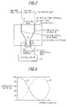
- FIG.1 shows the generalized composition of a conventional optical device thus developed.
- This optical device is composed of a first optical waveguide 11 and a second optical waveguide 12 on a LiNbO 3 substrate 10.
- the first optical waveguide 11 and the second optical waveguide 12 have same width, thickness and refractive index, and are disposed in parallel close to each other, thereby forming a directional coupler 13 in this parallel part.
- the coupling length that the movement of light between optical waveguides in the directional coupler 13 becomes 100% is defined as a perfect coupling length Lc.
- the directional coupler 13 is formed with a coupling length that is half of the perfect coupling length Lc.
- a total reflection film (or total reflection plate) 14 is disposed opposed to the end faces of the first and second optical waveguides forming the directional coupler 13. Further, on the first and second optical waveguides 11, 12 forming the directional coupler 13, control electrodes 15, 16 are formed through buffer layers (not shown), and voltage can be applied to its both ends.
- the optical energy of incident light 17 supplied to the first optical waveguide 11 of this optical device gradually moves to the second optical waveguide 12 in the directional coupler 13. Then, when propagating by half of the perfect coupling length Lc to reach the total reflection film 14, half of the energy of incident light is moved to the second optical waveguide 12. At this time, the first and second optical waveguides 11, 12 have a same optical intensity, and have phases inverse to each other. It reflects totally on the total reflection film 14, then propagating through the directional coupler 13 in the reverse direction. Also in this case, the optical energy gradually moves to the second optical waveguide 12. When returning to the incidence point of the directional coupler 13, all the optical energy is moved to the second optical waveguide 12. As a result, emitting light 18 with the same optical intensity as incident light 17 is obtained from the second optical waveguide 12.
- this optical device is composed of the first and second optical waveguides 11, 12 on the LiNbO 3 substrate 10.
- the substrate 10 has an electro-optic effect, where the refractive index at the periphery of voltage-applied part varies by electric field occurred by the application of voltage.
- applying voltage to the control electrodes 15, 16, the refractive index of the first and second optical waveguides 11, 12 formed under the electrodes can be changed.
- the coupling state between the optical waveguides changes due to the discordance of phase speed between the waveguide modes of the optical waveguides forming the directional coupler 13.
- light 18 can be controlled so as not to be emitted from the second optical waveguide 12.
- the optical device to perform such control can be miniaturized since it only has to have half of the perfect coupling length.
- Such optical devices using the electro-optic effect are, for example, disclosed in Japanese patent application laid-open Nos.63-234227(1988) and 3-256028(1991).
- optical devices have to use a very specific substrate with the electro-optic effect, e.g., LiNbO 3 substrate. Therefore, there is a problem that especially in combining and integrating various kinds of optical devices, the manufacturing cost increases.
- the present invention provides an optical device comprising:
- an optical device comprises:
- an optical device comprises:
- an optical device comprises:
- an optical device comprises:
- FIG.2 shows the generalized composition of an optical device in the first preferred embodiment according to the invention.
- This optical device is composed of a first optical waveguide 21 and a second optical waveguide 22 formed on a substrate 20 that is of quartz glass as the base material. Light is supplied to or emitted from a first port 23 and a second port 24 provided at the end face of the substrate 20.
- the first and second optical waveguides 21, 22 have same width, thickness and refractive index.
- the first and second optical waveguides 21, 22 are disposed in parallel close to each other, thereby forming a directional coupler 25 in this parallel part.
- the directional coupler 25 is formed with a coupling length that is half of the perfect coupling length Lc. The end of this coupling length contacts the end face of the substrate 20, and a total reflection film 26 is disposed opposed to the end faces of the optical waveguides.
- control electrodes 27, 28 are formed, and electric power is supplied from a control circuit 29.
- optical fiber terminals 30, 31 are coupled abutting on the ports, optionally using micro-optics technology to couple through lens to the port, to give such an optical wiring that optical signal is coupled efficiently.
- the coupling length of the directional coupler 25 is represented as L.
- the coupling length L is equal to the perfect coupling length Lc, the optical energy propagating the first optical waveguide 21 gradually moves to the second optical waveguide 22, and all the energy is perfectly moved at the end surface of the substrate 20 to which the end of coupling length of the directional coupler 25 faces.
- the coupling length L of the directional coupler 25 formed on the substrate 20 of the optical device is formed half of the perfect coupling length Lc, at the end face of the substrate 20 to which the end of the coupling length of the directional coupler 25 faces, half of the optical energy propagating the first optical waveguide 21 is moved to the second optical waveguide.
- the total reflection film 26 is disposed opposed to the end surface of the substrate 20 to which the directional coupler 25 faces, the signal light propagating the first optical waveguide 21 is totally reflected, again returned through the first and second optical waveguides 21, 22 forming the directional coupler 25.
- the optical energy gradually moves to the second optical waveguide 22.
- all the optical energy is moved. In this case, emitting light 33 with a same optical intensity as incident light 32 is propagated through the second optical waveguide 22, emitted from the second port 24.
- the coupling length of the directional coupler 25 becomes equal to the perfect coupling length Lc by the total reflection of the total reflection film 26, therefore the emitting light 33 is output from the second port 24.
- the condition that the distribution ratio ⁇ becomes 1 is that the coupling length L of the directional coupler 25 is equal to half of the perfect coupling length Lc.
- the perfect coupling length Lc is determined by various factors, one of which is the refractive indexes n of the first and second optical waveguides 21, 22 forming the directional coupler 25. It is known that the refractive index n of optical waveguide can be easily altered by external factors, e.g., a mechanical stress, heat and electric field applied to the waveguide substrate. So, by altering the external factors intentionally, the refractive index n can be altered to adjust the distribution ratio ⁇ .
- the optical device in FIG.2 is composed of the optical waveguides formed on the substrate 20 that is of quartz glass as the base material. Since such a quartz waveguide has a "thermo-optical effect" that the refractive index can be altered by heating, it is most efficient to use a heating system as means for adjusting the refractive index n. So, through the control electrodes 27, 28 for heating that are formed just over or around the first and second optical waveguides forming the directional coupler 25, electric power can be supplied from the control circuit 29. By such a composition, only the circumference of the waveguides can be heated locally.
- the refractive index n varies according to electric power supplied from the control electrodes 27, 28 for heating in the directional coupler 25, and as the result, the perfect coupling length Ls also varies.
- incident light 32 supplied to the first port 23 is propagated through the first optical waveguide 21, and the optical energy according to the varied perfect coupling length Lc moves to the second optical waveguide 22 side.
- the total reflection film 26 After being totally reflected by the total reflection film 26, it returns through the directional coupler 25 and emitting lights 34 and 33 are output from the first and second optical waveguides 21 and 22, respectively.
- the sum of the optical energy of emitting light 33 and the optical energy of emitting light 34 is equal to the optical energy of incident light 32.
- the output distributions of emitting lights 33, 34 can be altered arbitrarily, and therefore the distribution ratio ⁇ can be adjusted.
- FIG.3 shows the relationship between electric power supplied from the control electrodes 27, 28 required for heating to generate the thermo-optical effect of the optical device in FIG.2 and the distribution ratio ⁇ .
- the lateral axis indicates applied electric power [W] and the vertical axis indicates the distribution ratio ⁇ [%].
- a waveform 35 represents the distribution ratio ⁇ to emitting light 33 shown in expression (1)
- a waveform 36 represents the distribution ratio ⁇ ' to emitting light 34. Namely, the distribution ratio ⁇ ' is given by dividing the optical energy of emitting light 34 by the sum of the optical energy of emitting light 33 and the optical energy of emitting light 34.
- the optical waveguides are formed on the substrate of quartz glass as the base material.
- the directional coupler 25 with the evanescent-coupled coupling length L that is half of the perfect coupling length Lc, where the end of the coupling length faces to the end face of the substrate 20, and the total reflection film 26 disposed opposed to the end face of the waveguide.
- the control electrodes 27, 28 just over or around the first and second optical waveguides 21, 22 forming the directional coupler 25. Heating it locally, the refractive index n of the optical waveguide of the directional coupler 25 is altered.
- the perfect coupling length Lc can be altered and therefore the energy distribution of lights emitted from the directional coupler 25 can be altered.
- the integration can be realized at a lower manufacturing cost than conventional one. Further, by using part of the directional coupler repeatedly, the optical device can be miniaturized and electric power required to generate the thermo-optical effect can be halved.
- FIG.4 shows the generalized composition of an optical device in the second preferred embodiment according to the invention.
- the optical device in the second embodiment is composed so that emitting light 33 output from the second port 24 of the optical device in the first embodiment in FIG.2 can be monitored and electric power supplied can be altered by applying the control electrodes 27, 28 according to the monitored result.
- the first and second optical waveguides 21, 22 are formed on the substrate 20 that is of quartz glass as the base material. Light is supplied to or emitted from the first port 23 and the second port 24 provided at the end face of the substrate 20.
- the first and second optical waveguides 21, 22 have same width, thickness and refractive index.
- the first and second optical waveguides 21, 22 are disposed in parallel close to each other, thereby forming the directional coupler 25 in this parallel part.
- the directional coupler 25 is formed with a coupling length that is half of the perfect coupling length Lc. The end of this coupling length contacts the end face of the substrate 20, and the total reflection film 26 is disposed opposed to the end faces of the optical waveguides.
- control electrodes 27, 28 are formed, and electric power is supplied from a control circuit 41.
- the optical fiber terminal 30 is coupled abutting on the port, optionally using micro-optics technology to couple through lens to the port, to give such an optical wiring that optical signal is coupled efficiently.
- a photo diode (hereinafter referred to as 'PD') 40 is disposed directly.
- the monitoring results of PD 40 are input to the control circuit 41.
- the energy movement between the optical waveguides evanescent-coupled according to electric power supplied from the control circuit 41 is performed similarly to that in the first embodiment. Therefore, the explanations are omitted here.
- emitting light output from the second port 24 is input to PD 40, and therefore the optical energy of light emitted as emitting light 33 can be detected as the received light energy of PD 40.
- the intensity of light 34 emitted from the first port 23 can be adjusted to a desired value.
- the intensity of signal light received by PD 40 can be adjusted.
- PD 40 is disposed directly.
- Light emitted propagating through the second optical waveguide 22 is monitored by PD 40.
- the intensity of light emitted from the first optical waveguide 21 or the second optical waveguide 22 can be adjusted to a desired value.
- such an optical device can be used for the level adjustment of signal light in an optical fiber transmission system.
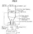
- FIG.5 shows the generalized composition of an optical device in the third preferred embodiment according to the invention.
- the optical device in the third embodiment is provided with high-reflectivity film (or high-reflectivityplate) 42, which is not total reflection film, that is disposed opposed to the end face of the optical waveguide of the substrate 20 where the coupling length of the directional coupler 25 contacts.
- the high-reflectivity film 42 transmits part of signal light propagating through the directional coupler 25 by the coupling length L to reach the end face of the optical waveguide of the substrate 20, and reflects the rest.
- the level of signal light transmitted through the high-reflectivity film 42 is detected by PD 43, and then feedbacked as the monitoring result to the control circuit 44.
- the first and second optical waveguides 21, 22 are formed on the substrate 20 that is of quartz glass as the base material. Light is supplied to or emitted from the first port 23 and the second port 24 provided at the end face of the substrate 20.
- the first and second optical waveguides 21, 22 have same width, thickness and refractive index.
- the first and second optical waveguides 21, 22 are disposed in parallel close to each other, thereby forming the directional coupler 25 in this parallel part.
- the directional coupler 25 is formed with a coupling length that is half of the perfect coupling length Lc. The end of this coupling length contacts the end face of the substrate 20, and the high-reflectivity film 42 is disposed opposed to the end faces of the optical waveguides. Signal light transmitted through the high-reflectivity film 42 is input to PD 43.
- control electrodes 27, 28 are formed, and electric power is supplied from a control circuit 44 according to the received light result of PD 43 to receive signal light transmitting through the high-reflectivity film 42.
- the optical fiber terminals 30, 31 are coupled abutting on the ports, optionally using micro-optics technology to couple through lens to the port, to give such an optical wiring that optical signal is coupled efficiently.
- the energy movement between the optical waveguides evanescent-coupled according to electric power supplied from the control circuit 44 is performed similarly to that in the first embodiment. Therefore, the explanations are omitted here.
- the high-reflectivity film 42 transmits part of signal light propagating through the directional coupler 25 and the optical intensity of transmitted light is then detected by PD 43. Therefore, electric power supplied from the control circuit 44 to the control electrodes 27, 28 can be altered according to the monitoring result of optical intensity detected by PD 43. Also, it can be detected whether incident light 32 supplied to the first port 23 is in the off-state or not. Moreover, the intensity of emitting light 33, 34 emitted from the first or second port 23, 24 can be adjusted nearly to a desired value.
- the high-reflectivity film 42 is disposed opposed to the end face of the optical waveguide of the substrate 20 where the end of the coupling length of the directional coupler 25 contacts.
- Light transmitted through the high-reflectivity film 42 is monitored, which allows the control circuit 44 to be controlled. Thereby, it can be detected whether incident light 32 supplied to the first port 23 is in the off-state or not. Even when the level of incident light 32 is abruptly varied in controlling constantly either of emitting lights 33, 34, the intensity of either of emitting lights 33, 34 can be adjusted nearly to a desired value.
- such an optical device can be used for the monitoring of signal light in an optical fiber transmission system.
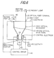
- FIG.6 shows the generalized composition of an optical device in the fourth preferred embodiment according to the invention.
- the optical device in the fourth embodiment monitors light 33 emitted from the second port 24. Further, it is provided with high-reflectivity film 42, which is not total reflection film, that is disposed opposed to the end face of the optical waveguide of the substrate 20 where the coupling length of the directional coupler 25 contacts. Light transmitting through the high-reflectivity film 42 is also monitored. According to the monitoring results of emitting light 33 and transmitted light of the high-reflectivity film 42, electric power supplied from a control circuit 45 to the control electrodes 27, 28 can be altered.
- the first and second optical waveguides 21, 22 are formed on the substrate 20 that is of quartz glass as the base material. Light is supplied to or emitted from the first port 23 and the second port 24 provided at the end face of the substrate 20.
- the first and second optical waveguides 21, 22 have same width, thickness and refractive index.
- the first and second optical waveguides 21, 22 are disposed in parallel close to each other, thereby forming the directional coupler 25 in this parallel part.
- the directional coupler 25 is formed with a coupling length that is half of the perfect coupling length Lc. The end of this coupling length contacts the end face of the substrate 20, and the high-reflectivity film 42 is disposed opposed to the end faces of the optical waveguides. Signal light transmitted through the high-reflectivity film 42 is input to PD 43.
- control electrodes 27, 28 are formed, and electric power is supplied from a control circuit 45.
- the optical fiber terminal 30 is coupled abutting on the port, optionally using micro-optics technology to couple through lens to the port, to give such an optical wiring that optical signal is coupled efficiently.
- PD 40 is disposed directly.
- the monitoring result of PD 40 is input to the control circuit 45.
- the control circuit 45 supplies electric power according to the received light result of PD 43 to receive signal light transmitting through the high-reflectivity film 42 and the received light result of PD 40 disposed directly at the second port 24.
- the energy movement between the optical waveguides evanescent-coupled according to electric power supplied from the control circuit 45 is performed similarly to that in the first embodiment. Therefore, the explanations are omitted here.
- the high-reflectivity film 42 transmits part of signal light propagating through the directional coupler 25 and the optical intensity of transmitted light is then detected by PD 43. Also, the optical intensity of light emitted from the second port 24 is detected by PD 40. Therefore, electric power supplied from the control circuit 45 to the control electrodes 27, 28 can be altered according to the monitoring result of optical intensity detected by PD 43. Thereby, it can be detected that incident light 32 supplied to the first port 23 is in the off-state. Further, even when the level of incident light 32 is varied abruptly, emitting light with a desired intensity to be controlled constant in advance can be output. Also, by altering electric power supplied from the control circuit 45 to the control electrodes 27, 28 according to the monitoring result of optical intensity detected by PD 40, the intensity of emitting light 33 emitted from the first optical waveguide 21 can be adjusted precisely to a desired value.
- the high-reflectivity film 42 is disposed opposed to the end face of the optical waveguide of the substrate 20 where the end of the coupling length of the directional coupler 25 contacts.
- Light transmitted through the high-reflectivity film 42 is monitored, which allows the control circuit 45 to be controlled.
- light emitted propagating through the second optical waveguide 22 is monitored by PD 40 disposed directly at the second port 24, and the monitoring result is feedbacked to control the control circuit 45.
- PD 40 disposed directly at the second port 24
- the monitoring result is feedbacked to control the control circuit 45.
- FIG.7 shows the generalized composition of an optical device in the fifth preferred embodiment according to the invention.
- the optical device in the fifth embodiment is provided with an optical amplifier 50 to amplify the optical intensity at a predetermined amplification, an optical circulator 51 to which light amplified by the optical amplifier 50 is input, and an optical amplifier 52 to which light output from the optical circulator 51 is input. Further, the optical circulator 51 is connected to an arrayed waveguide grating (hereinafter referred to as 'AWG') 53.
- 'AWG' arrayed waveguide grating
- AWG 53 can output demultiplexing light input from the optical circulator 51 into N optical fibers 54 1 to 54 N for wavelength components, and can multiplex the respective optical signals input from the N optical fibers 54 1 to 54 N , outputting it to the optical circulator 51.
- the optical fibers 54 1 to 54 N are connected with the first port 23 of the optical device in the fourth embodiment in FIG.6. This optical device is controlled so that, as described in the fourth embodiment, it can output light with a predetermined optical intensity even when incident light is varied abruptly.
- Amplified light from the optical amplifier 50 is input to the optical circulator 51.
- the optical circulator 51 outputs light input from the optical amplifier 50 to AWG 53.
- AWG 53 the respective wavelength components are input through the optical fibers 54 1 to 54 N to the optical device. Since this optical device can control incident light to be output again with a predetermined optical intensity, light with the optical intensity adjusted as described above is output to AWG 53.
- AWG 53 optical signals with wavelength components thus adjusted to a desired signal intensity and returned again are multiplexed, and then are output to the optical circulator 51.
- the optical circulator 51 outputs light input from AWG 53 to the optical amplifier 52.
- a repeater in optical fiber transmission system can repeat amplifying optical signal, but the signal levels of all wavelength components cannot be always kept constant by the optical intensity of optical amplifier since some optical elements have a wavelength-dependent characteristic.
- the wavelength-dependent characteristic of optical element causes a deterioration in reliability. So, as described above, between the optical amplifiers, the wavelength components are demultiplexed, each component being adjusted to have a desired signal intensity, then multiplexed again. Thereby, each of the wavelength components can have a predetermined optical intensity and therefore a high-quality transmission system can be obtained.
- an adjustable optical attenuator or a total reflector requires a very-large mounting area since it is necessary for each wavelength component. In this embodiment, so miniaturized devices can be provided. Further, comparing with the conventional adjustable optical attenuator, the consumption power can be halved.
- FIG.8 shows the generalized composition of an optical device in the first modification.
- like parts are indicated by like reference numerals as used in FIG.4 (second embodiment) and their explanations are omitted here.
- incident light 32 is supplied through an optical isolator 56. Also, emitting light from the second port 24 is divided by an optical divider 55, one is output as emitting light 33 and the other is input to PD 40, enabling the control circuit 41 to be controlled.
- the optical isolator and optical divider that prevent light from reflecting into waveguide can be used. Thereby, the precision in controlling optical intensity can be enhanced.
- FIG.9 shows the generalized composition of an arrayed optical device.
- a substrate 60 that is of quartz glass as the base material
- same optical devices 61 1 to 61 M are arrayed.
- Total reflection film 62 is disposed opposed to the end face where the coupling length of directional couplers contacts. Thereby, it is so miniaturized.
- high-reflectivity film other than the total reflection film can be disposed, where transmitted lights can be detected for controlling. Further, the total reflection film and high-reflectivity film may be arrayed in mixture.
- optical devices in the first to fifth embodiments described above can be arrayed as optical devices 61 1 to 61 M , and the total reflection film and/or high-reflectivity film may be disposed opposed to the end face where the coupling length of directional couplers contacts.
- the optical devices in the first to fifth embodiments described above can be arrayed as optical devices 61 1 to 61 M , and the total reflection film and/or high-reflectivity film may be disposed opposed to the end face where the coupling length of directional couplers contacts.
- optical devices described above can be used to control signal light to a constant level while being disposed on an optical transmission line, or can be applied to part of WAG, adjustable optical attenuator or reflector.
- the inventor attains the miniaturization that the mounting area is reduced to one tenth of conventional one by disposing the optical device(s) on one waveguide substrate. Also, since the coupling length of directional coupler is made half of the perfect coupling length, the heat release value is halved, thereby a device such a cooling plate can be miniaturized. Further, due to the miniaturization of device and the reduction in manufacturing cost because of arraying, the cost is lowered to about one third, comparing with when assembling conventionally the respective components.
- An optical device which has: a first optical waveguide disposed on a substrate having a thermo-optical effect; a second optical waveguide that, at its one end, has part which is disposed close to and in parallel with part of the first optical waveguide by a predetermined length on the substrate, and that, at the parallel part, is evanescent-coupled with light propagating through the first optical waveguide; light reflector that is disposed opposed to the end faces, at the one end, of the first and second optical waveguides and that totally reflects light emitted from the end faces; and distribution ratio altering system that heats around the evanescent-coupled parallel part of the first and second optical waveguides to alter a distribution ratio of lights emitted from the other ends of the first and second optical waveguides to which incident light supplied to the first optical waveguide at the other end is distributed.
Landscapes
- Physics & Mathematics (AREA)
- Nonlinear Science (AREA)
- General Physics & Mathematics (AREA)
- Optics & Photonics (AREA)
- Optical Integrated Circuits (AREA)
- Optical Modulation, Optical Deflection, Nonlinear Optics, Optical Demodulation, Optical Logic Elements (AREA)
Applications Claiming Priority (2)
| Application Number | Priority Date | Filing Date | Title |
|---|---|---|---|
| JP16438298A JP3257510B2 (ja) | 1998-05-29 | 1998-05-29 | 光デバイス |
| JP16438298 | 1998-05-29 |
Publications (1)
| Publication Number | Publication Date |
|---|---|
| EP0964290A1 true EP0964290A1 (de) | 1999-12-15 |
Family
ID=15792075
Family Applications (1)
| Application Number | Title | Priority Date | Filing Date |
|---|---|---|---|
| EP99304098A Withdrawn EP0964290A1 (de) | 1998-05-29 | 1999-05-26 | Optischer Schalter |
Country Status (3)
| Country | Link |
|---|---|
| US (1) | US6304697B1 (de) |
| EP (1) | EP0964290A1 (de) |
| JP (1) | JP3257510B2 (de) |
Cited By (3)
| Publication number | Priority date | Publication date | Assignee | Title |
|---|---|---|---|---|
| WO2003084008A3 (en) * | 2002-03-29 | 2004-03-18 | Teem Photonics | Integrated photonic devices having folded directional couplers |
| US6954564B2 (en) | 2000-11-27 | 2005-10-11 | Teem Photonics | Apparatus and method for integrated photonic devices having high-performance waveguides and multicompositional substrates |
| WO2014199384A1 (en) * | 2013-06-12 | 2014-12-18 | Corning Optical Communications Wireless, Ltd. | Voltage controlled optical directional coupler |
Families Citing this family (9)
| Publication number | Priority date | Publication date | Assignee | Title |
|---|---|---|---|---|
| WO2003044568A2 (en) * | 2001-11-19 | 2003-05-30 | Photon-X, Inc. | Optical amplifier with gain flattening filter |
| US6909824B1 (en) * | 2002-03-05 | 2005-06-21 | Avi Messica | Mechanically actuated evanescent-wave coupled optical devices |
| US6956998B2 (en) * | 2002-08-22 | 2005-10-18 | Prima Luci, Inc. | Compact optical delay lines |
| US20030185514A1 (en) * | 2002-03-29 | 2003-10-02 | Bendett Mark P. | Method and apparatus for tapping a waveguide on a substrate |
| JP4393456B2 (ja) * | 2003-06-25 | 2010-01-06 | 富士通株式会社 | 光増幅装置 |
| US7492992B1 (en) * | 2003-08-08 | 2009-02-17 | Neophotonics Corporation | Bi-directional PLC transceiver device |
| EP2866000B1 (de) * | 2013-10-22 | 2020-03-11 | Commissariat à l'Énergie Atomique et aux Énergies Alternatives | Optomechanische Vorrichtung zum Betätigen und/oder Erkennen einer Bewegung eines mechanischen Elements, insbesondere für die gravimetrische Erfassung |
| CN110601685B (zh) * | 2019-09-20 | 2025-01-07 | 浙江光塔安全科技有限公司 | 一种光开关装置、照明系统 |
| FR3143778B1 (fr) * | 2022-12-19 | 2024-12-13 | Commissariat Energie Atomique | Dispositif de rétro-propagation multiniveaux |
Citations (3)
| Publication number | Priority date | Publication date | Assignee | Title |
|---|---|---|---|---|
| JPS63234227A (ja) * | 1987-03-23 | 1988-09-29 | Matsushita Electric Ind Co Ltd | 方向性結合型光スイツチ |
| JPH03256028A (ja) * | 1990-03-06 | 1991-11-14 | Nec Corp | 光制御デバイス |
| EP0457406A1 (de) * | 1990-05-17 | 1991-11-21 | Koninklijke KPN N.V. | Digitaler optischer Schalter |
Family Cites Families (9)
| Publication number | Priority date | Publication date | Assignee | Title |
|---|---|---|---|---|
| JPS60192913A (ja) | 1984-03-14 | 1985-10-01 | Omron Tateisi Electronics Co | 導波形光反射装置 |
| JP2664749B2 (ja) | 1988-12-20 | 1997-10-22 | 富士通株式会社 | 光変調装置 |
| JPH052116A (ja) | 1991-06-17 | 1993-01-08 | Nippon Telegr & Teleph Corp <Ntt> | 光導波路 |
| US5361157A (en) * | 1992-08-25 | 1994-11-01 | Nippon Hoso Kyokai | Bidirectional light transmission system and optical device therefor |
| US5566263A (en) * | 1995-03-22 | 1996-10-15 | Minnesota Mining And Manufacturing Company | System for tuning an integrated optical switch element |
| JP3092499B2 (ja) * | 1995-12-04 | 2000-09-25 | 日本電気株式会社 | 導波路型光合波分波モジュール |
| JP2993433B2 (ja) * | 1996-08-02 | 1999-12-20 | 日本電気株式会社 | 光結合器 |
| US5886807A (en) * | 1997-01-24 | 1999-03-23 | California Institute Of Technology | Traveling-wave reflective electro-optic modulator |
| US5966493A (en) * | 1998-02-20 | 1999-10-12 | Molecular Optoelectronics Corporation | Fiber optic attenuators and attenuation systems |
-
1998
- 1998-05-29 JP JP16438298A patent/JP3257510B2/ja not_active Expired - Fee Related
-
1999
- 1999-05-21 US US09/315,965 patent/US6304697B1/en not_active Expired - Fee Related
- 1999-05-26 EP EP99304098A patent/EP0964290A1/de not_active Withdrawn
Patent Citations (3)
| Publication number | Priority date | Publication date | Assignee | Title |
|---|---|---|---|---|
| JPS63234227A (ja) * | 1987-03-23 | 1988-09-29 | Matsushita Electric Ind Co Ltd | 方向性結合型光スイツチ |
| JPH03256028A (ja) * | 1990-03-06 | 1991-11-14 | Nec Corp | 光制御デバイス |
| EP0457406A1 (de) * | 1990-05-17 | 1991-11-21 | Koninklijke KPN N.V. | Digitaler optischer Schalter |
Non-Patent Citations (3)
| Title |
|---|
| KAWACHI M: "RECENT PROGRESS IN SILICA-BASED PLANAR LIGHTWAVE CIRCUITS ON SILICON", IEE PROCEEDINGS: OPTOELECTRONICS, vol. 143, no. 5, 1 October 1996 (1996-10-01), pages 257 - 262, XP000680738 * |
| PATENT ABSTRACTS OF JAPAN vol. 013, no. 037 (P - 819) 27 January 1989 (1989-01-27) * |
| PATENT ABSTRACTS OF JAPAN vol. 016, no. 058 (P - 1311) 13 February 1992 (1992-02-13) * |
Cited By (5)
| Publication number | Priority date | Publication date | Assignee | Title |
|---|---|---|---|---|
| US6954564B2 (en) | 2000-11-27 | 2005-10-11 | Teem Photonics | Apparatus and method for integrated photonic devices having high-performance waveguides and multicompositional substrates |
| WO2003084008A3 (en) * | 2002-03-29 | 2004-03-18 | Teem Photonics | Integrated photonic devices having folded directional couplers |
| US6813405B1 (en) | 2002-03-29 | 2004-11-02 | Teem Photonics | Compact apparatus and method for integrated photonic devices having folded directional couplers |
| WO2014199384A1 (en) * | 2013-06-12 | 2014-12-18 | Corning Optical Communications Wireless, Ltd. | Voltage controlled optical directional coupler |
| US9715157B2 (en) | 2013-06-12 | 2017-07-25 | Corning Optical Communications Wireless Ltd | Voltage controlled optical directional coupler |
Also Published As
| Publication number | Publication date |
|---|---|
| US6304697B1 (en) | 2001-10-16 |
| JP3257510B2 (ja) | 2002-02-18 |
| JPH11344631A (ja) | 1999-12-14 |
Similar Documents
| Publication | Publication Date | Title |
|---|---|---|
| US6487336B1 (en) | WDM channel equalization and control | |
| US5970201A (en) | Power regulation in optical networks | |
| US6628850B1 (en) | Dynamic wavelength-selective grating modulator | |
| EP2659301B1 (de) | Optischer verstärker für mehrkern-glasfasern | |
| JP2993433B2 (ja) | 光結合器 | |
| US6304697B1 (en) | Thermo-optic device with evanescent wave coupling | |
| CA2364290A1 (en) | Dynamic gain flattening filter | |
| JP2000111816A (ja) | 能動整合フォトニクス組立体 | |
| US6031950A (en) | Wavelength-selective optical device having an adjustable grating for reducing transmission losses | |
| US9103987B2 (en) | Optical amplifier for multi-core optical fiber | |
| US6507680B1 (en) | Planar lightwave circuit module | |
| WO2020059639A1 (ja) | 光回路および光接続構造体 | |
| CN1316769C (zh) | 用于偏振模式色散补偿的系统 | |
| EP0518570B1 (de) | Optische Wellenlängenmultiplexmodule | |
| US7310460B2 (en) | Optical device | |
| Tong | Multiwavelength receivers for WDM systems | |
| EP1698922A2 (de) | Farbloser abstimmbarer Dispersionskompensator mit planarer Lichtwellenschaltung und deformierbarem Spiegel | |
| EP1841277A2 (de) | Multiportschalter für einen optischen Leistungsmonitor | |
| US7062120B2 (en) | Optical device and movable reflector | |
| US6064503A (en) | Light source for wavelength division multiplexing communications | |
| US7711222B2 (en) | Tunable dispersion compensation apparatus | |
| US20030068119A1 (en) | Mismatched mode field diameter device | |
| US6584271B2 (en) | Dual fiber variable optical attenuator | |
| EP1085354A2 (de) | Planares Lichtwellen Schaltungsmodul | |
| EP1055959A2 (de) | Temperaturabhängiger optischer Dämpfungsregler |
Legal Events
| Date | Code | Title | Description |
|---|---|---|---|
| PUAI | Public reference made under article 153(3) epc to a published international application that has entered the european phase |
Free format text: ORIGINAL CODE: 0009012 |
|
| 17P | Request for examination filed |
Effective date: 19990826 |
|
| AK | Designated contracting states |
Kind code of ref document: A1 Designated state(s): FR GB IT |
|
| AX | Request for extension of the european patent |
Free format text: AL;LT;LV;MK;RO;SI |
|
| AKX | Designation fees paid |
Free format text: FR GB IT |
|
| REG | Reference to a national code |
Ref country code: DE Ref legal event code: 8566 |
|
| 17Q | First examination report despatched |
Effective date: 20010122 |
|
| GRAG | Despatch of communication of intention to grant |
Free format text: ORIGINAL CODE: EPIDOS AGRA |
|
| GRAG | Despatch of communication of intention to grant |
Free format text: ORIGINAL CODE: EPIDOS AGRA |
|
| GRAH | Despatch of communication of intention to grant a patent |
Free format text: ORIGINAL CODE: EPIDOS IGRA |
|
| GRAH | Despatch of communication of intention to grant a patent |
Free format text: ORIGINAL CODE: EPIDOS IGRA |
|
| STAA | Information on the status of an ep patent application or granted ep patent |
Free format text: STATUS: THE APPLICATION IS DEEMED TO BE WITHDRAWN |
|
| 18D | Application deemed to be withdrawn |
Effective date: 20021203 |