EP0964337A1 - Verbindungsstruktur zum Datenaustausch zwischen verschiedenen adressierbaren Geräten eines Mikrorechners - Google Patents
Verbindungsstruktur zum Datenaustausch zwischen verschiedenen adressierbaren Geräten eines Mikrorechners Download PDFInfo
- Publication number
- EP0964337A1 EP0964337A1 EP99401441A EP99401441A EP0964337A1 EP 0964337 A1 EP0964337 A1 EP 0964337A1 EP 99401441 A EP99401441 A EP 99401441A EP 99401441 A EP99401441 A EP 99401441A EP 0964337 A1 EP0964337 A1 EP 0964337A1
- Authority
- EP
- European Patent Office
- Prior art keywords
- ring
- microcomputer
- interconnection
- coupling
- artery
- Prior art date
- Legal status (The legal status is an assumption and is not a legal conclusion. Google has not performed a legal analysis and makes no representation as to the accuracy of the status listed.)
- Granted
Links
Images
Classifications
-
- G—PHYSICS
- G06—COMPUTING OR CALCULATING; COUNTING
- G06F—ELECTRIC DIGITAL DATA PROCESSING
- G06F13/00—Interconnection of, or transfer of information or other signals between, memories, input/output devices or central processing units
- G06F13/38—Information transfer, e.g. on bus
- G06F13/40—Bus structure
- G06F13/4004—Coupling between buses
- G06F13/4022—Coupling between buses using switching circuits, e.g. switching matrix, connection or expansion network
Definitions
- the present invention relates to interconnection structures for the exchange of data between the various addressable parts of a microcomputer, in particular the microcomputer of a medical device active implantable such as a pacemaker or defibrillator.
- the consumption of the microcomputer is a factor that must be carefully mastered, because it has a direct impact on the lifespan of the implant, i.e. the number of years after which intervention will be required to exchange the implant, which has reached the end of its life.
- RAMs random access memories
- ROMs read-only memories
- DMA direct memory access
- interrupt management elements etc.
- the typical structure of such an interconnection artery is that of bidirectional bus on which all the components of the microcomputer are connected. Data exchange can take place in one direction, for example from the central processing unit to a memory for a write instruction, or in the opposite direction, for example from a memory to the central unit for a read instruction.
- a two-way bus connected to many organs implies, from the electrical point of view, a significant capacity compared to ground.
- This parasitic capacity will on the one hand increase the time required to modify the logical state of the common artery, because of the time required by the drivers to charge it of buses, thus leading to increasingly longer bus cycles. Else part and above all, the charge and discharge of this capacity at each logical state change will significantly increase consumption energy of the circuit.
- the drivers of bidirectional buses know three states, namely '1', '0' and a high impedance state, the latter corresponding no data flow on the bus, i.e. an unmanned state of the latter.
- a bus segment is in a high impedance state because floating inputs on CMOS circuits would lead to high currents going against of research into the current economy.
- One of the aims of the invention is to remedy these various drawbacks, by proposing an interconnection structure avoiding the use of a bidirectional bus, the latter structure being, as we have indicated, ill-suited to circuits that are both complex, miniaturized and low consumption.
- the interconnection structure of the invention comprises an interconnection route ensuring parallel transfer on a group conductors of the information to be exchanged, configured in at least a ring on which information circulates in a closed loop and unidirectionally, this artery comprising a plurality of points of coupling to the organs of the microcomputer.
- the coupling points include a gateway to, and from, another lower order ring, ring on which information flows also in closed loop and unidirectionally, so to constitute a structure comprising a plurality of hierarchical rings between them.
- the order ring includes the higher a point of coupling to a central processing unit.
- the gateway advantageously comprises means multiplexers for selectively forwarding on the order ring higher is the information received from the lower order ring, if the coupling point corresponding to the organ addressed is on this lower order ring or on an even lower order ring coupled to the latter, that is, the information received from the higher-order ring upstream, otherwise.
- the coupling points include a register associated with the corresponding member of the microcomputer, in particular with multiplexer means for selectively transferring downstream on the ring be the contents of the register, if the point of coupling corresponds to the device addressed, i.e. the information received from the ring upstream, otherwise.
- One of the coupling points can be a coupling point to a bus bidirectional data exchange, this coupling point then being preference located on the highest order ring and immediately preceding the central processing unit on this ring.
- the conductors of the interconnection artery operate in two-level logic, essentially stateless with high impedance.
- the circuit of the microcomputer has an implantation topology in which the organs belonging to the same ring are grouped on a common domain, this domain being adjacent to the area corresponding to the ring of the same rank immediately next, or previous, in the direction of information flow.
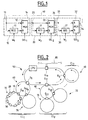
- Figure 1 schematically illustrates an elementary ring of the interconnection structure according to the invention.
- FIG. 2 shows a structure according to the invention, comprising a plurality of rings associated in a hierarchical structure.
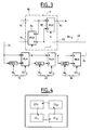
- Figure 3 shows how can be inserted on the loop in Figure 1 a coupling gateway with a higher order ring.
- FIG. 4 illustrates a preferential topology of implantation of the various circuits of a structure such as that of FIG. 2.
- This elementary configuration comprises a plurality of stages 10, 20, 30 (here three in number, this number being of course in no way limitative and a ring that can include a much higher number of floors).
- Each stage 10, 20, 30 has a register 11, 21, 31 and a multiplexer 12, 22, 32 with two inputs A, B and one output.
- registers and multiplexers are all made up of a group of conductors to which are transferred information in parallel, for example groups of eight conductors (eight-bit vectorized information), represented by a single line on the drawings.
- Each register 11, 21, 31 can designate an addressable organ of a microcomputer such as RAM, ROM, access interface DMA, interrupt management, timeout registers, etc.
- Each register has a separate input port and output port, each of the ports being unidirectional (entry or exit) and operates in two-state logic, i.e. is not likely to take an indefinite state with high impedance.
- Input 13, 23, 33 of each stage 10, 20, 30 is applied simultaneously on the one hand to the port of entry of the respective register 11, 21, 31 and on the other hand to one, A, of the input ports of the respective multiplexer 12, 22, 32.
- the other input, B, of the multiplexer is connected to the output port of the associated register.
- a control logic activates the write signals W 1 , W 2 , W 3 of the registers 11, 21, 31 and of the selection signals SEL 1 , SEL 2 , SEL 3 of the multiplexers 12, 22, 32.
- Output 14 of stage 10 (output port of multiplexer 12) is applied at entrance 23 of stage 20
- exit 24 of stage 20 (exit port of the multiplexer 22) is applied to the input 33 of the stage 30
- the output 34 of stage 30 (output port of multiplexer 32) is returned at the entrance 13 of the floor 10 by a line 40, so as to constitute a closed ring on which data can flow unidirectionally (i.e. from floor 10 to floor 20, then from floor 20 to floor 30, then from floor 30 to floor 10, and so on, but never in the opposite direction).
- the signal the corresponding SEL selection of the multiplexer is not activated and the multiplexer simply transfers (selection of port A) the content applied at the entrance of the floor at the exit of this same floor, then at the entrance from the next floor.
- control unit is designed to maintain the state of the SEL selection signals used during the last cycle to which the ring was addressed and, when no ring register has not been addressed, the last SEL selection signal is maintained activated ("last accessed" principle).
- the corresponding SEL selection signal of the multiplexer is activated (selection of port B), so that the multiplexer transfers the contents of the register towards the exit of the floor considered, which is thus applied on the next floor.
- the write signal W is also activated, indicating to the register addressed that it is necessary to lock the data applied at the entrance to the floor.
- the invention proposes to associate them, by an appropriate coupling, a plurality of rings so as to constitute a structure hierarchical.
- Figure 2 illustrates such a hierarchical structure.
- the highest level is a closed unidirectional ring 50, which we will call “root ring” to which is coupled the central unit of CPU processing.
- gateways or gateways G 1 , G 2 ... G N a plurality of rings or groups of rings organized in a cluster or clusters CL 1 , CL 2 ... CL N.
- a cluster may consist of a single isolated ring 60, as illustrated for the cluster CL N , the hierarchy then comprising for this cluster only two levels (root ring 50 and end ring 60).
- a cluster can also be constituted, as illustrated for the clusters CL 1 and CL 2 , of a ring 60 also comprising gateways such as G 11 , G 12 or G 21 , G 22 towards rings 70 of even lower level, the hierarchy then comprising for these clusters three levels in this example (rings 50, 60 and 70).
- the stages 10, 20, 30 ... associated with each of the addressable organs of the microcomputer are located on the lower level rings, the intermediate level rings being preferably (but not necessarily) only transition rings with only gateways to the upper and lower levels.
- FIG. 3 illustrates the structure of a gateway G allowing the transfer of data between two levels of the hierarchy.
- the basic structure of the ring is essentially the same as that of FIG. 1, with a plurality of stages 10, 20, 30 associated each to an addressable organ of the microcomputer, with the difference that we insert the gateway G on the return conductor 40 connecting exit 34 of the top floor of the ring to entry 13 of the first floor of this same ring.
- the gateway G consists of a floor 90 comprising an entrance 91 from the higher order ring, an exit 92 to destination from this same higher-order ring, an input 93 from of the lower order ring (connected to exit 34 of floor 30) and an output 94 to this same lower order ring (connected at entrance 13 of the first floor 10).
- the circuit comprises two multiplexers 95, 96 with two inputs A and B, controlled by a common single selection signal SEL 0 .
- Input signal 91 is applied to input A of multiplexer 95 and input B of multiplexer 96
- input 93 is applied to input B of multiplexer 95 and input A of multiplexer 96
- the output 92 is connected to the output of the multiplexer 95, and the output 94 to the output of the multiplexer 96.
- the two multiplexers will transfer to their respective outputs the signal present on their inputs A, so that the signals will flow without change separately on each of the two rings.
- the input 91 will be connected to the output 94 and the input 93 to the output 92, so that the upstream signal coming from the ring of higher order will be transferred on the the lower order ring at the entry of the first stage 10, and the signal collected at the exit of the last stage 30 of the lower order ring will be applied downstream to the higher order ring.
- the selection signal SEL 0 is activated each time any one of the stages of the lower order ring is addressed, that is to say, in the example illustrated, each time one of the signals SEL 1 , SEL 2 or SEL 3 is activated.
- the control logic of the different gateways can be designed so that only the segments (rings) of the data path necessary to convey data from a source register of a ring to a destination register of another ring actually have need to change state. In this case, all other segments of data located elsewhere in the cluster hierarchy is entirely static and consume no transition energy.
- a typical programmable pacemaker chip DDD has around 160 different registers to access (DMA, timer registers, interrupt management registers, etc.) 31 RAMs and 12 different ROMs.
- the number of organs per ring is chosen so as to achieve a compromise between, on the one hand, the food economy sought (by multiplying the number of rings we increase the resulting selectivity hierarchical structure, and therefore its performance) and the complexity system implementation. In practice, we can locate the optimum to approximately 6 to 10, typically 8, organs addressable by ring.
- this hierarchical cluster structure allows the addition new addressable organs in the hierarchy without modification substantial overall consumption of the circuit or access time to the organs already present.
- the root ring 50 its structure is adapted to its particular position. It contains the central processing unit CPU of the microcomputer and the gateways G 1 , G 2 , G N to all the clusters of the system. Furthermore, to ensure exchanges with the outside world, a special gateway G IO is provided, ensuring the interfacing between the root ring 50 and a bidirectional bus 80 of the conventional type necessary for interfacing with other chips, for example. example of standard memories and peripheral management circuits.
- the selection signals of the gateways G 1 , G 2 , G N , G IO of the root ring 50 these must be ordered separately in order to allow the data to propagate on the root ring at the times for the write and read operations of the central unit, and it is in particular for this reason that the gateway G IO is positioned just before the central unit CPU, in the direction of data propagation.
- the circuits of the different clusters CL 1 , CL 2 , CL 3 are grouped together in the same respective domains, and these domains are placed on the circuit so that the domain corresponding to a given cluster is adjacent to the domain corresponding to the immediately following cluster, etc. in order to minimize the physical lengths of the conductor, taking into account the direction of information flow within the same cluster and from one cluster to the next.
Landscapes
- Engineering & Computer Science (AREA)
- Physics & Mathematics (AREA)
- General Engineering & Computer Science (AREA)
- Theoretical Computer Science (AREA)
- Mathematical Physics (AREA)
- Computer Hardware Design (AREA)
- General Physics & Mathematics (AREA)
- Electrotherapy Devices (AREA)
- Power Sources (AREA)
- Microcomputers (AREA)
Applications Claiming Priority (2)
| Application Number | Priority Date | Filing Date | Title |
|---|---|---|---|
| FR9807431A FR2779844B1 (fr) | 1998-06-12 | 1998-06-12 | Structure d'interconnexion entre organes adressables d'un microcalculateur, notamment pour dispositif medical implantable actif tel que stimulateur ou defibrillateur cardiaque |
| FR9807431 | 1998-06-12 |
Publications (2)
| Publication Number | Publication Date |
|---|---|
| EP0964337A1 true EP0964337A1 (de) | 1999-12-15 |
| EP0964337B1 EP0964337B1 (de) | 2011-01-12 |
Family
ID=9527322
Family Applications (1)
| Application Number | Title | Priority Date | Filing Date |
|---|---|---|---|
| EP99401441A Expired - Lifetime EP0964337B1 (de) | 1998-06-12 | 1999-06-11 | Verbindungsstruktur zum Datenaustausch zwischen verschiedenen adressierbaren Geräten eines Mikrorechners |
Country Status (5)
| Country | Link |
|---|---|
| US (1) | US6532238B1 (de) |
| EP (1) | EP0964337B1 (de) |
| JP (1) | JP4711476B2 (de) |
| DE (1) | DE69943119D1 (de) |
| FR (1) | FR2779844B1 (de) |
Families Citing this family (3)
| Publication number | Priority date | Publication date | Assignee | Title |
|---|---|---|---|---|
| US6992975B1 (en) * | 2000-08-15 | 2006-01-31 | Cisco Technology, Inc. | Multiple ring support within a single network element |
| EP1324543A1 (de) * | 2001-12-26 | 2003-07-02 | Alcatel | Verfahren zum Schutz von RPR Netzen mit erweiterter Topologie, insbesondere RPR Ring zu Ring und vermaschte Hauptnetze |
| US8175703B2 (en) * | 2006-01-25 | 2012-05-08 | Cardiac Pacemakers, Inc. | Cardiac resynchronization therapy parameter optimization |
Citations (3)
| Publication number | Priority date | Publication date | Assignee | Title |
|---|---|---|---|---|
| WO1990016026A1 (en) * | 1989-06-20 | 1990-12-27 | Halley Systems, Inc. | Local area network bridge module |
| US4999832A (en) * | 1989-11-27 | 1991-03-12 | At&T Bell Laboratories | Broadband multirate switching architecture |
| EP0691767A2 (de) * | 1988-08-12 | 1996-01-10 | Digital Equipment Corporation | Mechanismus zur Paketentfernung in Token-Ring-Netzwerken |
Family Cites Families (2)
| Publication number | Priority date | Publication date | Assignee | Title |
|---|---|---|---|---|
| US6091705A (en) * | 1996-12-20 | 2000-07-18 | Sebring Systems, Inc. | Method and apparatus for a fault tolerant, software transparent and high data integrity extension to a backplane bus or interconnect |
| US6061335A (en) * | 1997-07-24 | 2000-05-09 | At&T Corp | Method for designing SONET ring networks suitable for local access |
-
1998
- 1998-06-12 FR FR9807431A patent/FR2779844B1/fr not_active Expired - Fee Related
-
1999
- 1999-06-11 EP EP99401441A patent/EP0964337B1/de not_active Expired - Lifetime
- 1999-06-11 US US09/332,281 patent/US6532238B1/en not_active Expired - Lifetime
- 1999-06-11 DE DE69943119T patent/DE69943119D1/de not_active Expired - Lifetime
- 1999-06-14 JP JP16689099A patent/JP4711476B2/ja not_active Expired - Lifetime
Patent Citations (3)
| Publication number | Priority date | Publication date | Assignee | Title |
|---|---|---|---|---|
| EP0691767A2 (de) * | 1988-08-12 | 1996-01-10 | Digital Equipment Corporation | Mechanismus zur Paketentfernung in Token-Ring-Netzwerken |
| WO1990016026A1 (en) * | 1989-06-20 | 1990-12-27 | Halley Systems, Inc. | Local area network bridge module |
| US4999832A (en) * | 1989-11-27 | 1991-03-12 | At&T Bell Laboratories | Broadband multirate switching architecture |
Also Published As
| Publication number | Publication date |
|---|---|
| US6532238B1 (en) | 2003-03-11 |
| FR2779844A1 (fr) | 1999-12-17 |
| JP4711476B2 (ja) | 2011-06-29 |
| EP0964337B1 (de) | 2011-01-12 |
| FR2779844B1 (fr) | 2001-07-27 |
| JP2000185108A (ja) | 2000-07-04 |
| DE69943119D1 (de) | 2011-02-24 |
Similar Documents
| Publication | Publication Date | Title |
|---|---|---|
| FR2979444A1 (fr) | Reseau sur puce extensible | |
| FR2824157A1 (fr) | Systeme de memoire evolutif avec interconnexions reconfigurables | |
| FR2472784A1 (fr) | Matrice de traitement de donnees en parallele, notamment pour l'analyse d'images prises par un satellite | |
| FR2600453A1 (fr) | Dispositif de memoire a semi-conducteurs | |
| EP0626760B1 (de) | Als Zellenmatrix-Netzwerk organisiertes elektronisches System | |
| FR2949879A1 (fr) | Noeuds d'entree/sortie d'un reseau sur puce torique. | |
| WO1993003441A1 (fr) | Architecture de systeme en tableau de processeurs a structure parallele | |
| FR3125614A1 (fr) | Dispositif informatique évolutif | |
| EP0964337A1 (de) | Verbindungsstruktur zum Datenaustausch zwischen verschiedenen adressierbaren Geräten eines Mikrorechners | |
| FR2948206A1 (fr) | Dispositif et procede pour l'execution distribuee de traitements de donnees numeriques | |
| FR2680262A1 (fr) | Circuits integres pour carte a puce et carte a plusieurs puces utilisant ces circuits. | |
| EP2043103B1 (de) | Elektronische Speichervorrichtung | |
| FR2732152A1 (fr) | Element de memoire du type bascule maitre-esclave, realise en technologie cmos | |
| FR2822581A1 (fr) | Procede et dispositif de transmission de donnees | |
| EP0634724A1 (de) | Verarbeitungssystem mit gemeinschaftlichem Speicher | |
| EP0437387A1 (de) | Integrierte Mikroprozessorschaltung mit intern-ROM- und extern-EPROM-Arbeitsweise | |
| EP0065460B1 (de) | Parallelzähler in integrierter MOS-Schaltung und seine Anwendung in einem Binäraddierer | |
| EP0109337A2 (de) | Datenverarbeitungsvorrichtung mit Multi-Mikrocomputer für Bildverarbeitung | |
| EP0359607A1 (de) | Zentrale Datenverarbeitungseinheit für ein Datenverarbeitungssystem | |
| EP0237425B1 (de) | Integrierter Schaltkreis von neuartiger Architektur und sein Hertellungsverfahren | |
| EP1398793B1 (de) | MOS technologische digital integrierte Schaltung | |
| FR2841680A1 (fr) | Dispositif de stockage de donnees multiports, en particulier pour une unte arithmetique et logique d'un processeur de traitement numerique du signal | |
| FR2699707A1 (fr) | Système informatique à haut débit, composant de mémoire et contrôleur de mémoire en résultant. | |
| EP1280206A1 (de) | ROM-Speicher | |
| EP1754162A2 (de) | Verfahren und vorrichtung zur busverwaltung |
Legal Events
| Date | Code | Title | Description |
|---|---|---|---|
| PUAI | Public reference made under article 153(3) epc to a published international application that has entered the european phase |
Free format text: ORIGINAL CODE: 0009012 |
|
| AK | Designated contracting states |
Kind code of ref document: A1 Designated state(s): BE CH DE FR GB IE IT LI SE |
|
| AX | Request for extension of the european patent |
Free format text: AL;LT;LV;MK;RO;SI |
|
| 17P | Request for examination filed |
Effective date: 20000513 |
|
| AKX | Designation fees paid |
Free format text: BE CH DE FR GB IE IT LI SE |
|
| 17Q | First examination report despatched |
Effective date: 20080819 |
|
| GRAP | Despatch of communication of intention to grant a patent |
Free format text: ORIGINAL CODE: EPIDOSNIGR1 |
|
| GRAS | Grant fee paid |
Free format text: ORIGINAL CODE: EPIDOSNIGR3 |
|
| GRAA | (expected) grant |
Free format text: ORIGINAL CODE: 0009210 |
|
| AK | Designated contracting states |
Kind code of ref document: B1 Designated state(s): BE CH DE FR GB IE IT LI SE |
|
| REG | Reference to a national code |
Ref country code: GB Ref legal event code: FG4D Free format text: NOT ENGLISH |
|
| REG | Reference to a national code |
Ref country code: CH Ref legal event code: EP |
|
| REG | Reference to a national code |
Ref country code: IE Ref legal event code: FG4D Free format text: LANGUAGE OF EP DOCUMENT: FRENCH |
|
| REF | Corresponds to: |
Ref document number: 69943119 Country of ref document: DE Date of ref document: 20110224 Kind code of ref document: P |
|
| REG | Reference to a national code |
Ref country code: DE Ref legal event code: R096 Ref document number: 69943119 Country of ref document: DE Effective date: 20110224 |
|
| REG | Reference to a national code |
Ref country code: SE Ref legal event code: TRGR |
|
| PLBE | No opposition filed within time limit |
Free format text: ORIGINAL CODE: 0009261 |
|
| STAA | Information on the status of an ep patent application or granted ep patent |
Free format text: STATUS: NO OPPOSITION FILED WITHIN TIME LIMIT |
|
| 26N | No opposition filed |
Effective date: 20111013 |
|
| BERE | Be: lapsed |
Owner name: ELA MEDICAL (SOCIETE ANONYME) Effective date: 20110630 |
|
| REG | Reference to a national code |
Ref country code: CH Ref legal event code: PL |
|
| REG | Reference to a national code |
Ref country code: DE Ref legal event code: R097 Ref document number: 69943119 Country of ref document: DE Effective date: 20111013 |
|
| PG25 | Lapsed in a contracting state [announced via postgrant information from national office to epo] |
Ref country code: BE Free format text: LAPSE BECAUSE OF NON-PAYMENT OF DUE FEES Effective date: 20110630 |
|
| PG25 | Lapsed in a contracting state [announced via postgrant information from national office to epo] |
Ref country code: LI Free format text: LAPSE BECAUSE OF NON-PAYMENT OF DUE FEES Effective date: 20110630 Ref country code: CH Free format text: LAPSE BECAUSE OF NON-PAYMENT OF DUE FEES Effective date: 20110630 |
|
| PGFP | Annual fee paid to national office [announced via postgrant information from national office to epo] |
Ref country code: IE Payment date: 20120612 Year of fee payment: 14 |
|
| PGFP | Annual fee paid to national office [announced via postgrant information from national office to epo] |
Ref country code: SE Payment date: 20120612 Year of fee payment: 14 |
|
| PG25 | Lapsed in a contracting state [announced via postgrant information from national office to epo] |
Ref country code: SE Free format text: LAPSE BECAUSE OF NON-PAYMENT OF DUE FEES Effective date: 20130612 |
|
| REG | Reference to a national code |
Ref country code: SE Ref legal event code: EUG |
|
| REG | Reference to a national code |
Ref country code: IE Ref legal event code: MM4A |
|
| PG25 | Lapsed in a contracting state [announced via postgrant information from national office to epo] |
Ref country code: IE Free format text: LAPSE BECAUSE OF NON-PAYMENT OF DUE FEES Effective date: 20130611 |
|
| REG | Reference to a national code |
Ref country code: FR Ref legal event code: PLFP Year of fee payment: 17 |
|
| PGFP | Annual fee paid to national office [announced via postgrant information from national office to epo] |
Ref country code: GB Payment date: 20150610 Year of fee payment: 17 Ref country code: DE Payment date: 20150602 Year of fee payment: 17 |
|
| PGFP | Annual fee paid to national office [announced via postgrant information from national office to epo] |
Ref country code: FR Payment date: 20150608 Year of fee payment: 17 |
|
| PGFP | Annual fee paid to national office [announced via postgrant information from national office to epo] |
Ref country code: IT Payment date: 20150625 Year of fee payment: 17 |
|
| REG | Reference to a national code |
Ref country code: DE Ref legal event code: R119 Ref document number: 69943119 Country of ref document: DE |
|
| GBPC | Gb: european patent ceased through non-payment of renewal fee |
Effective date: 20160611 |
|
| REG | Reference to a national code |
Ref country code: FR Ref legal event code: ST Effective date: 20170228 |
|
| PG25 | Lapsed in a contracting state [announced via postgrant information from national office to epo] |
Ref country code: FR Free format text: LAPSE BECAUSE OF NON-PAYMENT OF DUE FEES Effective date: 20160630 Ref country code: DE Free format text: LAPSE BECAUSE OF NON-PAYMENT OF DUE FEES Effective date: 20170103 |
|
| PG25 | Lapsed in a contracting state [announced via postgrant information from national office to epo] |
Ref country code: GB Free format text: LAPSE BECAUSE OF NON-PAYMENT OF DUE FEES Effective date: 20160611 |
|
| PG25 | Lapsed in a contracting state [announced via postgrant information from national office to epo] |
Ref country code: IT Free format text: LAPSE BECAUSE OF NON-PAYMENT OF DUE FEES Effective date: 20160611 |