EP0964441A2 - Ablagerung von Siliziumdioxid und Siliziumoxynitrid unter Gebrauch von Bis(tertiärbutylamino)silan - Google Patents
Ablagerung von Siliziumdioxid und Siliziumoxynitrid unter Gebrauch von Bis(tertiärbutylamino)silan Download PDFInfo
- Publication number
- EP0964441A2 EP0964441A2 EP99109396A EP99109396A EP0964441A2 EP 0964441 A2 EP0964441 A2 EP 0964441A2 EP 99109396 A EP99109396 A EP 99109396A EP 99109396 A EP99109396 A EP 99109396A EP 0964441 A2 EP0964441 A2 EP 0964441A2
- Authority
- EP
- European Patent Office
- Prior art keywords
- substrate
- silicon
- silane
- zone
- approximately
- Prior art date
- Legal status (The legal status is an assumption and is not a legal conclusion. Google has not performed a legal analysis and makes no representation as to the accuracy of the status listed.)
- Granted
Links
Images


Classifications
-
- B—PERFORMING OPERATIONS; TRANSPORTING
- B05—SPRAYING OR ATOMISING IN GENERAL; APPLYING FLUENT MATERIALS TO SURFACES, IN GENERAL
- B05D—PROCESSES FOR APPLYING FLUENT MATERIALS TO SURFACES, IN GENERAL
- B05D5/00—Processes for applying liquids or other fluent materials to surfaces to obtain special surface effects, finishes or structures
-
- H—ELECTRICITY
- H10—SEMICONDUCTOR DEVICES; ELECTRIC SOLID-STATE DEVICES NOT OTHERWISE PROVIDED FOR
- H10P—GENERIC PROCESSES OR APPARATUS FOR THE MANUFACTURE OR TREATMENT OF DEVICES COVERED BY CLASS H10
- H10P14/00—Formation of materials, e.g. in the shape of layers or pillars
- H10P14/60—Formation of materials, e.g. in the shape of layers or pillars of insulating materials
- H10P14/69—Inorganic materials
- H10P14/692—Inorganic materials composed of oxides, glassy oxides or oxide-based glasses
- H10P14/6921—Inorganic materials composed of oxides, glassy oxides or oxide-based glasses containing silicon
- H10P14/69215—Inorganic materials composed of oxides, glassy oxides or oxide-based glasses containing silicon the material being a silicon oxide, e.g. SiO2
-
- C—CHEMISTRY; METALLURGY
- C23—COATING METALLIC MATERIAL; COATING MATERIAL WITH METALLIC MATERIAL; CHEMICAL SURFACE TREATMENT; DIFFUSION TREATMENT OF METALLIC MATERIAL; COATING BY VACUUM EVAPORATION, BY SPUTTERING, BY ION IMPLANTATION OR BY CHEMICAL VAPOUR DEPOSITION, IN GENERAL; INHIBITING CORROSION OF METALLIC MATERIAL OR INCRUSTATION IN GENERAL
- C23C—COATING METALLIC MATERIAL; COATING MATERIAL WITH METALLIC MATERIAL; SURFACE TREATMENT OF METALLIC MATERIAL BY DIFFUSION INTO THE SURFACE, BY CHEMICAL CONVERSION OR SUBSTITUTION; COATING BY VACUUM EVAPORATION, BY SPUTTERING, BY ION IMPLANTATION OR BY CHEMICAL VAPOUR DEPOSITION, IN GENERAL
- C23C16/00—Chemical coating by decomposition of gaseous compounds, without leaving reaction products of surface material in the coating, i.e. chemical vapour deposition [CVD] processes
- C23C16/22—Chemical coating by decomposition of gaseous compounds, without leaving reaction products of surface material in the coating, i.e. chemical vapour deposition [CVD] processes characterised by the deposition of inorganic material, other than metallic material
- C23C16/30—Deposition of compounds, mixtures or solid solutions, e.g. borides, carbides, nitrides
- C23C16/308—Oxynitrides
-
- C—CHEMISTRY; METALLURGY
- C23—COATING METALLIC MATERIAL; COATING MATERIAL WITH METALLIC MATERIAL; CHEMICAL SURFACE TREATMENT; DIFFUSION TREATMENT OF METALLIC MATERIAL; COATING BY VACUUM EVAPORATION, BY SPUTTERING, BY ION IMPLANTATION OR BY CHEMICAL VAPOUR DEPOSITION, IN GENERAL; INHIBITING CORROSION OF METALLIC MATERIAL OR INCRUSTATION IN GENERAL
- C23C—COATING METALLIC MATERIAL; COATING MATERIAL WITH METALLIC MATERIAL; SURFACE TREATMENT OF METALLIC MATERIAL BY DIFFUSION INTO THE SURFACE, BY CHEMICAL CONVERSION OR SUBSTITUTION; COATING BY VACUUM EVAPORATION, BY SPUTTERING, BY ION IMPLANTATION OR BY CHEMICAL VAPOUR DEPOSITION, IN GENERAL
- C23C16/00—Chemical coating by decomposition of gaseous compounds, without leaving reaction products of surface material in the coating, i.e. chemical vapour deposition [CVD] processes
- C23C16/22—Chemical coating by decomposition of gaseous compounds, without leaving reaction products of surface material in the coating, i.e. chemical vapour deposition [CVD] processes characterised by the deposition of inorganic material, other than metallic material
- C23C16/30—Deposition of compounds, mixtures or solid solutions, e.g. borides, carbides, nitrides
- C23C16/40—Oxides
- C23C16/401—Oxides containing silicon
- C23C16/402—Silicon dioxide
-
- H—ELECTRICITY
- H10—SEMICONDUCTOR DEVICES; ELECTRIC SOLID-STATE DEVICES NOT OTHERWISE PROVIDED FOR
- H10P—GENERIC PROCESSES OR APPARATUS FOR THE MANUFACTURE OR TREATMENT OF DEVICES COVERED BY CLASS H10
- H10P14/00—Formation of materials, e.g. in the shape of layers or pillars
- H10P14/60—Formation of materials, e.g. in the shape of layers or pillars of insulating materials
- H10P14/63—Formation of materials, e.g. in the shape of layers or pillars of insulating materials characterised by the formation processes
- H10P14/6326—Deposition processes
- H10P14/6328—Deposition from the gas or vapour phase
- H10P14/6334—Deposition from the gas or vapour phase using decomposition or reaction of gaseous or vapour phase compounds, i.e. chemical vapour deposition
-
- H—ELECTRICITY
- H10—SEMICONDUCTOR DEVICES; ELECTRIC SOLID-STATE DEVICES NOT OTHERWISE PROVIDED FOR
- H10P—GENERIC PROCESSES OR APPARATUS FOR THE MANUFACTURE OR TREATMENT OF DEVICES COVERED BY CLASS H10
- H10P14/00—Formation of materials, e.g. in the shape of layers or pillars
- H10P14/60—Formation of materials, e.g. in the shape of layers or pillars of insulating materials
- H10P14/66—Formation of materials, e.g. in the shape of layers or pillars of insulating materials characterised by the type of materials
- H10P14/668—Formation of materials, e.g. in the shape of layers or pillars of insulating materials characterised by the type of materials the materials being characterised by the deposition precursor materials
- H10P14/6681—Formation of materials, e.g. in the shape of layers or pillars of insulating materials characterised by the type of materials the materials being characterised by the deposition precursor materials the precursor containing a compound comprising Si
- H10P14/6687—Formation of materials, e.g. in the shape of layers or pillars of insulating materials characterised by the type of materials the materials being characterised by the deposition precursor materials the precursor containing a compound comprising Si the compound comprising silicon and nitrogen
-
- H—ELECTRICITY
- H10—SEMICONDUCTOR DEVICES; ELECTRIC SOLID-STATE DEVICES NOT OTHERWISE PROVIDED FOR
- H10P—GENERIC PROCESSES OR APPARATUS FOR THE MANUFACTURE OR TREATMENT OF DEVICES COVERED BY CLASS H10
- H10P14/00—Formation of materials, e.g. in the shape of layers or pillars
- H10P14/60—Formation of materials, e.g. in the shape of layers or pillars of insulating materials
- H10P14/69—Inorganic materials
- H10P14/692—Inorganic materials composed of oxides, glassy oxides or oxide-based glasses
- H10P14/6921—Inorganic materials composed of oxides, glassy oxides or oxide-based glasses containing silicon
- H10P14/6922—Inorganic materials composed of oxides, glassy oxides or oxide-based glasses containing silicon the material containing Si, O and at least one of H, N, C, F or other non-metal elements, e.g. SiOC, SiOC:H or SiONC
- H10P14/6927—Inorganic materials composed of oxides, glassy oxides or oxide-based glasses containing silicon the material containing Si, O and at least one of H, N, C, F or other non-metal elements, e.g. SiOC, SiOC:H or SiONC the material being a silicon oxynitride, e.g. SiON or SiON:H
-
- H—ELECTRICITY
- H10—SEMICONDUCTOR DEVICES; ELECTRIC SOLID-STATE DEVICES NOT OTHERWISE PROVIDED FOR
- H10P—GENERIC PROCESSES OR APPARATUS FOR THE MANUFACTURE OR TREATMENT OF DEVICES COVERED BY CLASS H10
- H10P14/00—Formation of materials, e.g. in the shape of layers or pillars
- H10P14/60—Formation of materials, e.g. in the shape of layers or pillars of insulating materials
- H10P14/69—Inorganic materials
- H10P14/694—Inorganic materials composed of nitrides
- H10P14/6943—Inorganic materials composed of nitrides containing silicon
- H10P14/69433—Inorganic materials composed of nitrides containing silicon the material being a silicon nitride not containing oxygen, e.g. SixNy or SixByNz
Definitions
- the present invention is directed to the field of chemical vapor deposition of silicon dioxide and silicon oxynitride films using bis(tertiarybutylamino)silane, a novel organosilicon source material. It allows for the deposition of different dielectrics using the same organosilicon source, temperature, and pressure simply by varying reactant gases.
- a thin passive layer of a chemically inert dielectric material such as, silicon dioxide, silicon oxynitride and silicon nitride films, is essential. Thin layers of these dielectric films function as diffusion masks, oxidation barriers, trench isolation, intermetallic dielectric material with high dielectric breakdown voltages and as passivation layers.
- the present semiconductor industry standard for silicon dioxide and silicon oxynitride growth methods is by low pressure chemical vapor deposition in a hot wall reactor at >400°C.
- Deposition of silicon dioxide over large numbers of silicon wafers has been accomplished using silane and oxygen above 400°C, by dichlorosilane and N 2 O above 800°C, and by tetraethoxysilane above 650°C.
- Deposition of silicon oxynitride has been obtained using dichlorosilane, N 2 O and NH 3 above 750°C, see Semiconductor and Process technology handbook, edited by Gary E. McGuire, Noyes Publication, New Jersey, (1988), pp 289-301; and Silicon Processing for the VLSI ERA, Wolf Stanley, and Talbert, Richard N., Lattice Press, Sunset Beach, California (1990), pp 20-22, 327-330.
- Japanese Patent 6-132284 describes deposition of silicon nitride using organosilanes with a general formula (R 1 R 2 N) n SiH 4-n (where R 1 and R 2 range from H-, CH 3 -, C 2 H 5 - C 3 H 7- , C 4 H 9 -) by a plasma enhanced chemical vapor deposition and thermal chemical vapor deposition in the presence of ammonia or nitrogen.
- the precursors described here are tertiary amines and do not contain NH bonding as in the case of the present invention.
- the deposition experiments were carried out in a single wafer reactor at 400°C at high pressures of 80-100 Torr.
- the Si:N ratios in these films were 0.9 (Si:N ratios in Si 3 N 4 films is 0.75) with hydrogen content in the deposited films.
- the butyl radical is in the form of isobutyl.
- US Patent Application SN 08/942,996 filed 2 October 1997 discloses a process for the low pressure chemical vapor deposition of silicon nitride on a substrate using ammonia and a silane of the formula: (t-C 4 H 9 NH) 2 SiH 2 .
- the prior art has attempted to produce silicon dioxide or silicon oxynitride or silicon nitride films at temperatures >550C, at high deposition rates and low hydrogen and carbon contamination. However, the prior art has not been successful in achieving all these goals simultaneously with one silicon precursor.
- the present invention has overcome the problems of the prior art with the use of a single precursor for the formation of silicon dioxide and silicon oxynitride (as well as silicon nitride), which avoids the problems of plasma deposition, operates at low thermal conditions ( ⁇ 600C), avoids Si-C bonds to reduce carbon contamination of the resulting films, has low hydrogen contamination, as well as avoiding chlorine contamination and operates at low pressures (20 mTorr - 2 Torr) and up to atmospheric pressures in a manufacturable batch furnace (100 wafers or more) or a single wafer reactor, as will be described in greater detail below.
- the present invention is a process for the deposition on a substrate of a film of an oxygen containing silicon compound selected from the group consisting of silicon dioxide and silicon oxynitride by reacting bis(tertiarybutylamino)silane at an elevated temperature with a reactant gas selected from the group consisting of oxygen, ozone or mixtures thereof when the silicon compound is silicon dioxide or selected from the group consisting of a nitrogen oxide, ammonia and mixtures thereof when the silicon compound is silicon oxynitride.
- the bis(tertiarybutylamino)silane and O 2 or O 3 are allowed to react in the reactor tube at an elevated temperature, preferably 500°C-800°C.
- the bis(tertiarybutylamino)silane and N 2 O, NO 2 or NO with or without NH 3 are allowed to react in the reactor tube at an elevated temperature, preferably 500°C-800°C.
- the composition of the film to obtain desired O/N ratios can be easily accomplished by changing the ratios of the reactant gas mixtures as described in the experimental section.
- the pressure is in the range of approximately 20 mTorr to 1 atmosphere.
- the molar ratio of reactant gases O 2 , O 3 , N 2 O, NO, NO 2 , NH 3 or mixtures of gases to BTBAS is greater than approximately 1:1.
- the substrate is silicon.
- the substrate is an electronic device.
- the substrate is a flat panel display.
- the present invention is a chemical vapor deposition of silicon dioxide in a reaction zone, comprising the steps of:
- the present invention is a chemical vapor deposition of silicon oxynitride in a reaction zone, comprising the steps of:
- the present invention is a process for the chemical vapor deposition on a substrate of a stack of silicon compounds selected from the group consisting of silicon dioxide, silicon oxynitrides and silicon nitride in a reaction zone, comprising the steps of:
- VLSI Very Large Scale Integration
- These deposited thin films can be of metals, semiconductors, or insulators.
- the films may be thermally grown or deposited from the vapor phase using low pressure chemical vapor deposition (LPCVD).
- LPCVD low pressure chemical vapor deposition
- VLSI technology requires very thin insulators for a variety of applications in both microprocessors and random-access memories device fabrication.
- Silicon dioxide has been predominantly used as a dielectric material because of its ease of deposition and excellent properties at the SiO 2 /Si interface.
- Silicon nitride has other advantages over silicon dioxide, some of these include impurity and dopant resistant diffusion barriers, high dielectric breakdown voltages, superior mechanical and inherent inertness of Si 3 N 4 .
- Charge transport in metal nitride oxide and semiconductor (MNOS) devices can be reduced by depositing a thin layer of silicon oxynitride prior to silicon nitride deposition or by replacing silicon nitride with silicon oxynitride.
- MNOS metal nitride oxide and semiconductor
- the present invention is directed to bis(tertiarybutylamino)silanes as a class of aminosilanes that deposit silicon dioxide and silicon oxynitride at the same unexpectedly low temperatures with superior uniformities.
- the bis(tertiarybutylamino)silane has the following formula: (t-C 4 H 9 NH) 2 Si(H) 2 .
- the deposited films have superior uniformities and are free of ammonium chloride and chlorine contamination.
- Analogous aminosilanes which contain ligands, such as n-butylamines and tetrakis(dimethylamino)silane, do not deposit carbon free films at such low temperatures by LPCVD or otherwise, and the film uniformities are poorer.
- bis(tertiarybutylamino)silane may be attributable to the inherent property of t-butyl amine ligands in bis(tertiarybutylamino)silane.
- the t-butyl amine ligand may eliminate readily as isobutylene. Isobutylene is a very stable, good leaving group and thus does not contaminate films during deposition.
- tertiarybutylamino groups are more basic than dialkylamines due to the presence of the nitrogen-hydrogen bond (N-H) in the tertiarybutylamino group.
- N-H nitrogen-hydrogen bond
- the presence of the N-H bond may facilitate labile ⁇ -hydride transfer to form diaminosilane and cleavage of the tertiarybutyl group as isobutylene.
- the bis(tertiarybutylamino)silane compound is also more desirable than than the mono, tri or tetrakis (tertiarybutylamino) analog because the mono analog is unstable, the tri substituted analog has significant delivery problems, the tetrakis (tertiary butylamino)silane analog has much lower vapor pressure and cannot be readily synthesized due to steric bulk of the ligands on a single silicon atom and therefore inappropriate for commercial use.
- the N-H bonding properties discussed above is an added advantage in the case of when compared to other alkylaminosilane.
- the bis(tertiarybutylamino)silane and O 2 , O 3 or mixtures are allowed to react in the reactor tube at an elevated temperature, preferably 500°C-800°C.
- the bis(tertiarybutylamino)silane and N 2 O, NO 2 or NO plus NH 3 are allowed to react in the reactor tube at an elevated temperature, preferably 500°C-800°C.
- the O/N ratio in the silicon oxynitride can be varied by changing the ratios of reactant gases as desired.
- silicon dioxide is not formed by adding NO or N 2 O to BTBAS at these low temperatures, in contrast to oxide formation using dichlorosilane and N 2 O.
- each layer has a potentially discrete concentration of oxygen and nitrogen varying layer to layer from all silicon and oxygen in the form of silicon dioxide for a particular layer or layers, through various concentrations of silicon, oxygen and nitrogen in the form of silicon oxynitride for a particular layer or layers, to silicon and nitrogen in the form of silicon nitride for a particular layer or layers, can be deposited merely by varying the concentration of the reactant gases of O 2 , O 3 , N 2 O, NO, NO 2 , NH 3 and mixtures that react with the BTBAS for each layer in the stack which comprises the ultimately deposited film.
- the CVD process can be grouped into a) a gas-phase process and b) a surface reaction process.
- the gas phase phenomenon is the rate at which gases impinge on the substrate. This is modeled by the rate at which gases cross the boundary layer that separates the bulk regions of flowing gas and substrate surface. Such transport processes occur by gas-phase diffusion, which is proportional to the diffusivity of the gas and concentration gradient across the boundary layer.
- Several surface processes can be important when the gases reach the hot surface, but the surface reaction, in general, can be modeled by a thermally activated phenomenon which proceeds at a rate which is a function of the frequency factor, the activation energy, and the temperature.
- Reaction may occur either on the surface or very close to the wafer surface to deposit a thin film of silicon dioxide or silicon oxynitride, as required. If the reaction occurs in the gas phase (a homogeneous reaction) then clusters of silicon dioxide or silicon oxynitride are formed. When the reaction occurs close to the wafer surface then the resulting films are of superior uniformities. Thus, one important requirement for CVD application is the degree to which heterogeneous reactions are favored over gas phase reactions.
- the surface reaction rate increases with increasing temperature.
- the temperature may rise high enough so that the reaction rate exceeds the rate at which reactant species arrive at the surface. In such cases, the reaction cannot proceed any more rapidly than the rate at which reactant gases are supplied to the substrate by mass transport. This is referred to as a mass-transport limited deposition process.
- the surface reaction rate is reduced, and eventually the concentration of reactants exceeds the rate at which they are consumed by the surface reaction process. Under such conditions the deposition rate is reaction rate limited.
- the deposition is usually mass-transport limited, while at lower temperatures it is surface-reaction rate-limited.
- the temperature at which the deposition condition moves from one of these growth regimes to the other is dependent on the activation energy of the reaction, and the gas flow conditions in the reactor. Thus, it is difficult to extrapolate process conditions or results from one pressure regime or temperature regime to another.
- the temperature of the process is an important parameter. That is, uniform deposition rates throughout a reactor require conditions that maintain a constant reaction rate. This, in turn, implies that a constant temperature must exist everywhere on all wafer surfaces. On the other hand, under such conditions, the rate at which reactants reach the surface is not important, since their concentration does not limit the growth rate. Thus, it is not as critical that a reactor be designed to supply an equal flux of reactants to all locations of a wafer surface. It should be appreciated that in LPCVD reactors, wafers can be stacked vertically and at very close spacing because such systems operate in a reaction rate limited mode.
- LPCVD Low pressure chemical vapor deposition processes
- CVD chemical vapor deposition
- Horizontal tube hot wall reactors are the most widely used for LPCVD in VLSI manufacturing. They are employed for depositing poly-Si, silicon nitride and undoped and doped silicon dioxide films. These reactors are used extensively because they are economical, have high throughputs, their deposited films are uniform and they can accommodate large diameter wafers (6"-12"). Their main disadvantages are poor thermal uniformity over wafers greater than 150 mm diameter and difficulties in automation.
- the vertical flow isothermal LPCVD reactor may also be used for deposition of silicon dioxide. These reactors are more easily automated than horizontal reactors and produce more uniform temperatures across large diameter wafers.
- the vacuum system consisted of a rotary vane pump/roots blower combination and various cold traps.
- the reactor pressure is controlled by a capacitance manometer feedback to a throttle valve controller.
- Reactor loading consisted of eighty 100 mm diameter silicon wafers at 9mm spacing in standard diffusion boats. The boats were positioned on a sled, so that the wafers centers were slightly above the center of the reaction tube. This produces a uniform conductance around the wafer peripheries by compensating for conductance restrictions caused by the boats and the sled.
- the temperature uniformity across the wafer load for the data presented was ⁇ 1°C as measured by an internal multi-junction thermocouple. Deposition uniformity down the wafer load is improved by a temperature ramp.
- the present invention of a method of depositing substantially pure thin silicon dioxide and silicon oxynitride, films on silicon wafers by using a bis(tertiarybutylamino)silane precursor has been demonstrated experimentally.
- the bis(tertiarybutylamino)silane is a non-pyrophoric volatile liquid which is safer to handle than silane and dichlorosilane.
- the deposition process is carried out at low to atmospheric pressure, preferably 20mTorr-2Torr and at elevated temperature preferably in the temperature range of preferably 500°C to 800°C using vapors from bis(tertiarybutylamino)silane and reactant gases O 2 or O 3 for silicon dioxide or N 2 O, NO or NO 2 and NH 3 for silicon oxynitride.
- an inert gas diluent such as nitrogen or argon, can be used to dilute and control the rate of reaction.
- the molar feed ratio of reactant gases as mentioned above, to bis(tertiarybutylamino)silane and is preferably greater than 1:1.
- the process involves reaction of bis(tertiarybutylamino)silane with oxygen at 250 mTorr reactor pressure.
- the precursor and oxygen are introduced into the heated reactor (550-625°C)-at the door.
- the reactants are flowed over wafers into the evacuated chamber.
- the oxygen to silicon source is kept at a ratio in the range of 1.6:1-2:1.
- a continuous film of silicon dioxide is deposited upon the surface of a silicon wafer. These films are suitable for integrated circuit manufacture.
- a typical run was carried out in a 150mm hot wall LPCVD horizontal tube reactor, although the apparatus configuration is not critical.
- the process involves loading the quartz reactor with 75 to 100 silicon wafers; evacuating the system; letting the wafers come to a desired temperature at which the deposition will be carried out.
- the energy required for this reaction can be supplied by simple resistive heating.
- simple, resistive heating is advantageous because the equipment is less expensive, and one avoids radiative film damage often associated with plasma reactors.
- the films are characterized by infrared spectroscopy and refractive index.
- FT-IR spectrum is consistent with thermally grown silicon dioxide and silicon dioxide films deposited from other known oxide precursors e.g. dichlorosilane + N 2 O, tetraethoxysilane, and diethylsilane.
- oxide precursors e.g. dichlorosilane + N 2 O, tetraethoxysilane, and diethylsilane.
- Refractive indices for these films were measured by ellipsometry at 632.4 nm and the refractive indices ranged from 1.46 to 1.50 for these films.
- Figure 1 shows the temperature dependence of the silicon oxide deposition rate.
- BTBAS was flowed at a rate of 55 standard cubic centimeters per minute (sccm) and oxygen was flowed at 90 and 120 sccm. There were no significant differences in film deposition rates, refractive indices, or absorption bands associated with different oxygen flows. This shows that the process is very robust (unchanged by slight changes in variables).
- the process involves reaction of bis(tertiarybutylamino)silane with N 2 O and NH 3 at 600°C and 500 mTorr reactor pressure.
- the precursor and reactants are introduced into the heated reactor, as in Example 1.
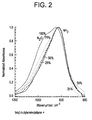
- the film properties could be varied from a silicon nitride to various silicon oxynitrides. This is shown in the FTIR spectra normalized in Figure 2.
- the percentages are of N 2 O in the mixture of N 2 O + NH 3 (total volumetric flow of 200 sccm).
- the average deposition rate varied from 20 to 29 Angstroms per minute, with higher rates occuring with higher percentages of N 2 O.
- Bis(tertiarybutylamino)silane has been shown to have superior properties and performance in depositing either silicon oxide or silicon oxynitride, as well as silicon nitride.
- High deposition rates are obtained using chemicals that have N-H bonds; i.e.,bis(tertiarybutylamino)silane.
- the lowest carbon impurities in deposited films are obtained using chemicals that do not have direct Si-C bonds, namely; bis(tertiarybutylamino)silane.
- the most uniform depositions are obtained using chemicals that have t-butyl groups, namely; bis(tertiarybutylamino)silane.
- bis(tertiarybutylamino)silane is unexpectedly a superior silicon oxide and silicon oxynitride precursor, as well as a silicon nitride precursor.
Landscapes
- Chemical & Material Sciences (AREA)
- Inorganic Chemistry (AREA)
- General Chemical & Material Sciences (AREA)
- Chemical Kinetics & Catalysis (AREA)
- Engineering & Computer Science (AREA)
- Materials Engineering (AREA)
- Mechanical Engineering (AREA)
- Metallurgy (AREA)
- Organic Chemistry (AREA)
- Formation Of Insulating Films (AREA)
- Chemical Vapour Deposition (AREA)
Applications Claiming Priority (2)
| Application Number | Priority Date | Filing Date | Title |
|---|---|---|---|
| US95818 | 1998-06-11 | ||
| US09/095,818 US5976991A (en) | 1998-06-11 | 1998-06-11 | Deposition of silicon dioxide and silicon oxynitride using bis(tertiarybutylamino) silane |
Publications (3)
| Publication Number | Publication Date |
|---|---|
| EP0964441A2 true EP0964441A2 (de) | 1999-12-15 |
| EP0964441A3 EP0964441A3 (de) | 2000-03-15 |
| EP0964441B1 EP0964441B1 (de) | 2002-05-02 |
Family
ID=22253723
Family Applications (1)
| Application Number | Title | Priority Date | Filing Date |
|---|---|---|---|
| EP99109396A Expired - Lifetime EP0964441B1 (de) | 1998-06-11 | 1999-06-02 | Ablagerung von Siliziumdioxid und Siliziumoxynitrid unter Gebrauch von Bis(tertiärbutylamino)silan |
Country Status (9)
| Country | Link |
|---|---|
| US (1) | US5976991A (de) |
| EP (1) | EP0964441B1 (de) |
| JP (1) | JP3055123B2 (de) |
| KR (1) | KR100323628B1 (de) |
| CN (1) | CN1138872C (de) |
| DE (1) | DE69901367T2 (de) |
| IL (1) | IL130310A (de) |
| SG (1) | SG71928A1 (de) |
| TW (1) | TW498109B (de) |
Cited By (1)
| Publication number | Priority date | Publication date | Assignee | Title |
|---|---|---|---|---|
| EP1535321A4 (de) * | 2002-08-18 | 2009-05-27 | Asml Us Inc | Niedertemperaturablagerung von siliziumoxiden und oxinitriden |
Families Citing this family (71)
| Publication number | Priority date | Publication date | Assignee | Title |
|---|---|---|---|---|
| US6235650B1 (en) * | 1997-12-29 | 2001-05-22 | Vanguard International Semiconductor Corporation | Method for improved semiconductor device reliability |
| US5976991A (en) | 1998-06-11 | 1999-11-02 | Air Products And Chemicals, Inc. | Deposition of silicon dioxide and silicon oxynitride using bis(tertiarybutylamino) silane |
| US6063666A (en) * | 1998-06-16 | 2000-05-16 | Advanced Micro Devices, Inc. | RTCVD oxide and N2 O anneal for top oxide of ONO film |
| KR100348591B1 (ko) | 1998-09-17 | 2002-08-13 | 가부시키가이샤 이시가키 | 연속 압착식 탈수장치 |
| US6251802B1 (en) | 1998-10-19 | 2001-06-26 | Micron Technology, Inc. | Methods of forming carbon-containing layers |
| US6462371B1 (en) * | 1998-11-24 | 2002-10-08 | Micron Technology Inc. | Films doped with carbon for use in integrated circuit technology |
| US6303520B1 (en) * | 1998-12-15 | 2001-10-16 | Mattson Technology, Inc. | Silicon oxynitride film |
| JP3819660B2 (ja) * | 2000-02-15 | 2006-09-13 | 株式会社日立国際電気 | 半導体装置の製造方法および半導体製造装置 |
| US6515350B1 (en) * | 2000-02-22 | 2003-02-04 | Micron Technology, Inc. | Protective conformal silicon nitride films and spacers |
| US6518626B1 (en) * | 2000-02-22 | 2003-02-11 | Micron Technology, Inc. | Method of forming low dielectric silicon oxynitride spacer films highly selective of etchants |
| US6429149B1 (en) | 2000-02-23 | 2002-08-06 | International Business Machines Corporation | Low temperature LPCVD PSG/BPSG process |
| US6486015B1 (en) * | 2000-04-25 | 2002-11-26 | Infineon Technologies Ag | Low temperature carbon rich oxy-nitride for improved RIE selectivity |
| KR100848423B1 (ko) * | 2000-09-19 | 2008-07-28 | 맷슨 테크놀로지, 인크. | 유전체 코팅 및 유전체 코팅을 형성하는 방법 |
| US6534388B1 (en) * | 2000-09-27 | 2003-03-18 | Chartered Semiconductor Manufacturing Ltd. | Method to reduce variation in LDD series resistance |
| EP1199743A3 (de) * | 2000-10-17 | 2004-06-30 | Texas Instruments Deutschland Gmbh | Methode zur Herstellung eines Schichtenstapels auf einem Halbleitersubtsrat bestehend aus einer Si3N4 Schicht und einer darüberliegenden SiO2 Schicht |
| DE10051382A1 (de) * | 2000-10-17 | 2002-05-02 | Texas Instruments Deutschland | Verfahren zum Herstellen eines Stapels aus einer Si¶3¶N¶4¶-Schicht und einer darüberliegenden Si0¶2¶-Schicht auf einem Halbleitersubstrat |
| US6500772B2 (en) * | 2001-01-08 | 2002-12-31 | International Business Machines Corporation | Methods and materials for depositing films on semiconductor substrates |
| US7005392B2 (en) * | 2001-03-30 | 2006-02-28 | Advanced Technology Materials, Inc. | Source reagent compositions for CVD formation of gate dielectric thin films using amide precursors and method of using same |
| US7084080B2 (en) * | 2001-03-30 | 2006-08-01 | Advanced Technology Materials, Inc. | Silicon source reagent compositions, and method of making and using same for microelectronic device structure |
| US20020182342A1 (en) * | 2001-04-13 | 2002-12-05 | Luc Ouellet | Optical quality silica films |
| JP4897159B2 (ja) * | 2001-08-03 | 2012-03-14 | 株式会社日立国際電気 | 半導体装置の製造方法 |
| US6670255B2 (en) * | 2001-09-27 | 2003-12-30 | International Business Machines Corporation | Method of fabricating lateral diodes and bipolar transistors |
| JP4021653B2 (ja) * | 2001-11-30 | 2007-12-12 | レール・リキード−ソシエテ・アノニム・プール・レテュード・エ・レクスプロワタシオン・デ・プロセデ・ジョルジュ・クロード | Cvd法によるシリコン窒化物膜またはシリコンオキシ窒化物膜の製造方法 |
| US6713127B2 (en) * | 2001-12-28 | 2004-03-30 | Applied Materials, Inc. | Methods for silicon oxide and oxynitride deposition using single wafer low pressure CVD |
| AU2003256559A1 (en) * | 2002-07-19 | 2004-02-09 | Aviza Technology, Inc. | Low temperature dielectric deposition using aminosilane and ozone |
| TW200424343A (en) * | 2002-09-05 | 2004-11-16 | Asml Us Inc | Low temperature deposition of silicon based thin films by single-wafer hot-wall rapid thermal chemical vapor deposition |
| JP4358492B2 (ja) * | 2002-09-25 | 2009-11-04 | レール・リキード−ソシエテ・アノニム・プール・レテュード・エ・レクスプロワタシオン・デ・プロセデ・ジョルジュ・クロード | 熱化学気相成長法によるシリコン窒化物膜またはシリコンオキシ窒化物膜の製造方法 |
| JP2004153066A (ja) | 2002-10-31 | 2004-05-27 | Fujitsu Ltd | 半導体装置の製造方法 |
| US6963006B2 (en) * | 2003-01-15 | 2005-11-08 | Air Products And Chemicals, Inc. | Process for the production and purification of bis(tertiary-butylamino)silane |
| US7122222B2 (en) * | 2003-01-23 | 2006-10-17 | Air Products And Chemicals, Inc. | Precursors for depositing silicon containing films and processes thereof |
| JP4954448B2 (ja) * | 2003-04-05 | 2012-06-13 | ローム・アンド・ハース・エレクトロニック・マテリアルズ,エル.エル.シー. | 有機金属化合物 |
| US7163860B1 (en) | 2003-05-06 | 2007-01-16 | Spansion Llc | Method of formation of gate stack spacer and charge storage materials having reduced hydrogen content in charge trapping dielectric flash memory device |
| JP3811697B2 (ja) * | 2003-11-19 | 2006-08-23 | 松下電器産業株式会社 | 半導体装置の製造方法 |
| JP4187252B2 (ja) | 2004-01-06 | 2008-11-26 | 富士通マイクロエレクトロニクス株式会社 | 半導体装置の製造方法 |
| US20050181633A1 (en) * | 2004-02-17 | 2005-08-18 | Hochberg Arthur K. | Precursors for depositing silicon-containing films and processes thereof |
| US7049200B2 (en) * | 2004-05-25 | 2006-05-23 | Applied Materials Inc. | Method for forming a low thermal budget spacer |
| US20050287747A1 (en) * | 2004-06-29 | 2005-12-29 | International Business Machines Corporation | Doped nitride film, doped oxide film and other doped films |
| US20060062913A1 (en) * | 2004-09-17 | 2006-03-23 | Yun-Ren Wang | Process for depositing btbas-based silicon nitride films |
| US20060182885A1 (en) * | 2005-02-14 | 2006-08-17 | Xinjian Lei | Preparation of metal silicon nitride films via cyclic deposition |
| US7875556B2 (en) * | 2005-05-16 | 2011-01-25 | Air Products And Chemicals, Inc. | Precursors for CVD silicon carbo-nitride and silicon nitride films |
| US7248758B2 (en) * | 2005-06-08 | 2007-07-24 | Verizon Business Global Llc | Hitless tunable filter |
| JP2006351694A (ja) * | 2005-06-14 | 2006-12-28 | Fujitsu Ltd | 半導体装置およびその製造方法 |
| US20070154637A1 (en) * | 2005-12-19 | 2007-07-05 | Rohm And Haas Electronic Materials Llc | Organometallic composition |
| JP5524443B2 (ja) * | 2006-03-24 | 2014-06-18 | ピーエスフォー ルクスコ エスエイアールエル | 半導体装置及びその製造方法 |
| US20070262399A1 (en) * | 2006-05-10 | 2007-11-15 | Gilbert Dewey | Sealing spacer to reduce or eliminate lateral oxidation of a high-k gate dielectric |
| US8530361B2 (en) | 2006-05-23 | 2013-09-10 | Air Products And Chemicals, Inc. | Process for producing silicon and oxide films from organoaminosilane precursors |
| US8318966B2 (en) * | 2006-06-23 | 2012-11-27 | Praxair Technology, Inc. | Organometallic compounds |
| US7956207B2 (en) * | 2006-09-28 | 2011-06-07 | Praxair Technology, Inc. | Heteroleptic organometallic compounds |
| US20080124946A1 (en) * | 2006-11-28 | 2008-05-29 | Air Products And Chemicals, Inc. | Organosilane compounds for modifying dielectrical properties of silicon oxide and silicon nitride films |
| US7678422B2 (en) * | 2006-12-13 | 2010-03-16 | Air Products And Chemicals, Inc. | Cyclic chemical vapor deposition of metal-silicon containing films |
| US20080145978A1 (en) * | 2006-12-18 | 2008-06-19 | Air Liquide Electronics U.S. Lp | Deposition of silicon germanium nitrogen precursors for strain engineering |
| US7750173B2 (en) | 2007-01-18 | 2010-07-06 | Advanced Technology Materials, Inc. | Tantalum amido-complexes with chelate ligands useful for CVD and ALD of TaN and Ta205 thin films |
| US20080207007A1 (en) | 2007-02-27 | 2008-08-28 | Air Products And Chemicals, Inc. | Plasma Enhanced Cyclic Chemical Vapor Deposition of Silicon-Containing Films |
| JP2008283051A (ja) * | 2007-05-11 | 2008-11-20 | Toshiba Corp | 半導体記憶装置及び半導体記憶装置の製造方法 |
| KR100956210B1 (ko) * | 2007-06-19 | 2010-05-04 | 에어 프로덕츠 앤드 케미칼스, 인코오포레이티드 | 금속 실리콘 질화물 박막의 플라즈마 강화 사이클릭증착방법 |
| US20090130414A1 (en) * | 2007-11-08 | 2009-05-21 | Air Products And Chemicals, Inc. | Preparation of A Metal-containing Film Via ALD or CVD Processes |
| US8298628B2 (en) | 2008-06-02 | 2012-10-30 | Air Products And Chemicals, Inc. | Low temperature deposition of silicon-containing films |
| US8058138B2 (en) * | 2008-07-17 | 2011-11-15 | Micron Technology, Inc. | Gap processing |
| US8148249B2 (en) * | 2008-09-12 | 2012-04-03 | Taiwan Semiconductor Manufacturing Company, Ltd. | Methods of fabricating high-k metal gate devices |
| WO2010065874A2 (en) | 2008-12-05 | 2010-06-10 | Atmi | High concentration nitrogen-containing germanium telluride based memory devices and processes of making |
| KR101706809B1 (ko) | 2010-03-26 | 2017-02-15 | 엔테그리스, 아이엔씨. | 게르마늄 안티몬 텔루라이드 물질 및 이를 포함하는 장치 |
| US9190609B2 (en) | 2010-05-21 | 2015-11-17 | Entegris, Inc. | Germanium antimony telluride materials and devices incorporating same |
| CN102011105B (zh) * | 2010-10-12 | 2014-06-04 | 上海宏力半导体制造有限公司 | 低压淀积氧化硅工艺方法 |
| US8460753B2 (en) * | 2010-12-09 | 2013-06-11 | Air Products And Chemicals, Inc. | Methods for depositing silicon dioxide or silicon oxide films using aminovinylsilanes |
| CN103958731B (zh) * | 2011-09-30 | 2016-12-21 | 阿科玛股份有限公司 | 通过常压化学气相沉积沉积氧化硅 |
| WO2014070682A1 (en) | 2012-10-30 | 2014-05-08 | Advaned Technology Materials, Inc. | Double self-aligned phase change memory device structure |
| CN104498895B (zh) * | 2014-12-23 | 2017-02-22 | 国家纳米科学中心 | 一种超薄氮氧化硅膜材料及其制备方法和用途 |
| KR20190114874A (ko) | 2018-03-30 | 2019-10-10 | 에스케이트리켐 주식회사 | 실리콘 박막 형성용 전구체 및 이를 이용한 실리콘 함유 박막 형성 방법 및 상기 실리콘 함유 박막을 포함하는 반도체 소자. |
| CN110459462B (zh) * | 2019-08-08 | 2022-02-15 | 武汉新芯集成电路制造有限公司 | 半导体器件的形成方法 |
| KR20210041809A (ko) | 2019-10-08 | 2021-04-16 | 에스케이트리켐 주식회사 | 실리콘 박막 형성용 전구체 및 이를 이용한 실리콘 박막 형성 방법 및 상기 실리콘 박막을 포함하는 반도체 소자. |
| CN111816556B (zh) * | 2020-06-03 | 2024-01-23 | 中国科学院微电子研究所 | 晶体管及制备方法 |
Family Cites Families (7)
| Publication number | Priority date | Publication date | Assignee | Title |
|---|---|---|---|---|
| US4992306A (en) * | 1990-02-01 | 1991-02-12 | Air Products Abd Chemicals, Inc. | Deposition of silicon dioxide and silicon oxynitride films using azidosilane sources |
| JP2637265B2 (ja) * | 1990-06-28 | 1997-08-06 | 株式会社東芝 | 窒化珪素膜の形成方法 |
| JPH04151839A (ja) * | 1990-10-16 | 1992-05-25 | Kawasaki Steel Corp | シリコンオキシナイトライド膜の製造方法 |
| US5459108A (en) * | 1992-10-06 | 1995-10-17 | Sharp Kabushiki Kaisha | Normal pressure CVD process for manufacture of a semiconductor device through reaction of a nitrogen containing organic source with ozone |
| JPH06132284A (ja) * | 1992-10-22 | 1994-05-13 | Kawasaki Steel Corp | 半導体装置の保護膜形成方法 |
| US5874368A (en) * | 1997-10-02 | 1999-02-23 | Air Products And Chemicals, Inc. | Silicon nitride from bis(tertiarybutylamino)silane |
| US5976991A (en) | 1998-06-11 | 1999-11-02 | Air Products And Chemicals, Inc. | Deposition of silicon dioxide and silicon oxynitride using bis(tertiarybutylamino) silane |
-
1998
- 1998-06-11 US US09/095,818 patent/US5976991A/en not_active Expired - Lifetime
-
1999
- 1999-06-02 EP EP99109396A patent/EP0964441B1/de not_active Expired - Lifetime
- 1999-06-02 DE DE69901367T patent/DE69901367T2/de not_active Expired - Lifetime
- 1999-06-02 SG SG1999002836A patent/SG71928A1/en unknown
- 1999-06-04 IL IL13031099A patent/IL130310A/xx not_active IP Right Cessation
- 1999-06-05 TW TW088109373A patent/TW498109B/zh not_active IP Right Cessation
- 1999-06-07 KR KR1019990020902A patent/KR100323628B1/ko not_active Expired - Lifetime
- 1999-06-10 JP JP11163791A patent/JP3055123B2/ja not_active Expired - Lifetime
- 1999-06-11 CN CNB991084594A patent/CN1138872C/zh not_active Expired - Lifetime
Cited By (1)
| Publication number | Priority date | Publication date | Assignee | Title |
|---|---|---|---|---|
| EP1535321A4 (de) * | 2002-08-18 | 2009-05-27 | Asml Us Inc | Niedertemperaturablagerung von siliziumoxiden und oxinitriden |
Also Published As
| Publication number | Publication date |
|---|---|
| SG71928A1 (en) | 2000-04-18 |
| KR100323628B1 (ko) | 2002-02-07 |
| EP0964441B1 (de) | 2002-05-02 |
| JP2000077403A (ja) | 2000-03-14 |
| US5976991A (en) | 1999-11-02 |
| IL130310A (en) | 2003-01-12 |
| IL130310A0 (en) | 2000-06-01 |
| DE69901367D1 (de) | 2002-06-06 |
| CN1138872C (zh) | 2004-02-18 |
| JP3055123B2 (ja) | 2000-06-26 |
| CN1239155A (zh) | 1999-12-22 |
| EP0964441A3 (de) | 2000-03-15 |
| TW498109B (en) | 2002-08-11 |
| KR20000005967A (ko) | 2000-01-25 |
| DE69901367T2 (de) | 2002-08-29 |
Similar Documents
| Publication | Publication Date | Title |
|---|---|---|
| EP0964441B1 (de) | Ablagerung von Siliziumdioxid und Siliziumoxynitrid unter Gebrauch von Bis(tertiärbutylamino)silan | |
| US5874368A (en) | Silicon nitride from bis(tertiarybutylamino)silane | |
| US7288145B2 (en) | Precursors for depositing silicon containing films | |
| US5744196A (en) | Low temperature deposition of silicon dioxide using organosilanes | |
| US5204141A (en) | Deposition of silicon dioxide films at temperatures as low as 100 degree c. by lpcvd using organodisilane sources | |
| US20050181633A1 (en) | Precursors for depositing silicon-containing films and processes thereof | |
| US9783558B2 (en) | Composition and method for low temperature chemical vapor deposition of silicon-containing films including silicon carbonitride and silicon oxycarbonitride films | |
| US4981724A (en) | Deposition of silicon oxide films using alkylsilane liquid sources | |
| EP1630249A2 (de) | Verfahren zur chemischen Gasphasenabscheidung von Siliziumnitrid. | |
| US20100285663A1 (en) | Composition and method for low temperature deposition of silicon-containing films such as films including silicon, silicon nitride, silicon dioxide and/or silicon-oxynitride | |
| US20100041243A1 (en) | Precursors for Depositing Silicon-containing Films and Methods for Making and Using Same | |
| US20070031598A1 (en) | Method for depositing silicon-containing films | |
| EP1713953A2 (de) | Verfahren zur herstellung von siliciumnitridfilmen und siliciumoxidnitridfilmen durch chemische dampfabscheidung | |
| KR100607979B1 (ko) | Hf 및 Zr 함유 옥시질화물 필름의 CVD 방법 | |
| US20060198958A1 (en) | Methods for producing silicon nitride films by vapor-phase growth | |
| HK1017390B (en) | Silicon nitride from bis (tertiarybutylamino) silane | |
| TWI246719B (en) | Low temperature deposition of silicon nitride |
Legal Events
| Date | Code | Title | Description |
|---|---|---|---|
| PUAI | Public reference made under article 153(3) epc to a published international application that has entered the european phase |
Free format text: ORIGINAL CODE: 0009012 |
|
| AK | Designated contracting states |
Kind code of ref document: A2 Designated state(s): BE DE ES FR GB IT NL |
|
| AX | Request for extension of the european patent |
Free format text: AL;LT;LV;MK;RO;SI |
|
| PUAL | Search report despatched |
Free format text: ORIGINAL CODE: 0009013 |
|
| AK | Designated contracting states |
Kind code of ref document: A3 Designated state(s): AT BE CH CY DE DK ES FI FR GB GR IE IT LI LU MC NL PT SE |
|
| AX | Request for extension of the european patent |
Free format text: AL;LT;LV;MK;RO;SI |
|
| RIC1 | Information provided on ipc code assigned before grant |
Free format text: 7H 01L 21/314 A, 7H 01L 21/316 B, 7C 23C 16/30 B, 7C 23C 16/40 B |
|
| 17P | Request for examination filed |
Effective date: 20000621 |
|
| 17Q | First examination report despatched |
Effective date: 20001005 |
|
| AKX | Designation fees paid |
Free format text: BE DE ES FR GB IT NL |
|
| GRAG | Despatch of communication of intention to grant |
Free format text: ORIGINAL CODE: EPIDOS AGRA |
|
| GRAG | Despatch of communication of intention to grant |
Free format text: ORIGINAL CODE: EPIDOS AGRA |
|
| GRAH | Despatch of communication of intention to grant a patent |
Free format text: ORIGINAL CODE: EPIDOS IGRA |
|
| REG | Reference to a national code |
Ref country code: GB Ref legal event code: IF02 |
|
| GRAH | Despatch of communication of intention to grant a patent |
Free format text: ORIGINAL CODE: EPIDOS IGRA |
|
| GRAA | (expected) grant |
Free format text: ORIGINAL CODE: 0009210 |
|
| AK | Designated contracting states |
Kind code of ref document: B1 Designated state(s): BE DE ES FR GB IT NL |
|
| PG25 | Lapsed in a contracting state [announced via postgrant information from national office to epo] |
Ref country code: BE Free format text: LAPSE BECAUSE OF FAILURE TO SUBMIT A TRANSLATION OF THE DESCRIPTION OR TO PAY THE FEE WITHIN THE PRESCRIBED TIME-LIMIT Effective date: 20020502 |
|
| REG | Reference to a national code |
Ref country code: GB Ref legal event code: FG4D |
|
| REF | Corresponds to: |
Ref document number: 69901367 Country of ref document: DE Date of ref document: 20020606 |
|
| ET | Fr: translation filed | ||
| PG25 | Lapsed in a contracting state [announced via postgrant information from national office to epo] |
Ref country code: ES Free format text: LAPSE BECAUSE OF FAILURE TO SUBMIT A TRANSLATION OF THE DESCRIPTION OR TO PAY THE FEE WITHIN THE PRESCRIBED TIME-LIMIT Effective date: 20021128 |
|
| PLBE | No opposition filed within time limit |
Free format text: ORIGINAL CODE: 0009261 |
|
| STAA | Information on the status of an ep patent application or granted ep patent |
Free format text: STATUS: NO OPPOSITION FILED WITHIN TIME LIMIT |
|
| 26N | No opposition filed |
Effective date: 20030204 |
|
| REG | Reference to a national code |
Ref country code: FR Ref legal event code: PLFP Year of fee payment: 17 |
|
| REG | Reference to a national code |
Ref country code: FR Ref legal event code: PLFP Year of fee payment: 18 |
|
| REG | Reference to a national code |
Ref country code: FR Ref legal event code: PLFP Year of fee payment: 19 |
|
| REG | Reference to a national code |
Ref country code: DE Ref legal event code: R082 Ref document number: 69901367 Country of ref document: DE Representative=s name: SSM SANDMAIR PATENTANWAELTE RECHTSANWALT PARTN, DE Ref country code: DE Ref legal event code: R082 Ref document number: 69901367 Country of ref document: DE Representative=s name: SCHWABE SANDMAIR MARX PATENTANWAELTE RECHTSANW, DE Ref country code: DE Ref legal event code: R081 Ref document number: 69901367 Country of ref document: DE Owner name: VERSUM MATERIALS US, LLC (N.D.GES. DES STAATES, US Free format text: FORMER OWNER: AIR PRODUCTS AND CHEMICALS, INC., ALLENTOWN, PA., US |
|
| REG | Reference to a national code |
Ref country code: GB Ref legal event code: 732E Free format text: REGISTERED BETWEEN 20171123 AND 20171129 |
|
| REG | Reference to a national code |
Ref country code: FR Ref legal event code: PLFP Year of fee payment: 20 |
|
| PGFP | Annual fee paid to national office [announced via postgrant information from national office to epo] |
Ref country code: DE Payment date: 20180522 Year of fee payment: 20 |
|
| PGFP | Annual fee paid to national office [announced via postgrant information from national office to epo] |
Ref country code: NL Payment date: 20180514 Year of fee payment: 20 Ref country code: FR Payment date: 20180411 Year of fee payment: 20 |
|
| PGFP | Annual fee paid to national office [announced via postgrant information from national office to epo] |
Ref country code: GB Payment date: 20180403 Year of fee payment: 20 Ref country code: IT Payment date: 20180625 Year of fee payment: 20 |
|
| REG | Reference to a national code |
Ref country code: NL Ref legal event code: PD Owner name: VERSUM MATERIALS US, LLC; US Free format text: DETAILS ASSIGNMENT: CHANGE OF OWNER(S), ASSIGNMENT; FORMER OWNER NAME: AIR PRODUCTS AND CHEMICALS, INC. Effective date: 20181221 |
|
| REG | Reference to a national code |
Ref country code: DE Ref legal event code: R071 Ref document number: 69901367 Country of ref document: DE |
|
| REG | Reference to a national code |
Ref country code: NL Ref legal event code: MK Effective date: 20190601 |
|
| REG | Reference to a national code |
Ref country code: GB Ref legal event code: PE20 Expiry date: 20190601 |
|
| PG25 | Lapsed in a contracting state [announced via postgrant information from national office to epo] |
Ref country code: GB Free format text: LAPSE BECAUSE OF EXPIRATION OF PROTECTION Effective date: 20190601 |