EP0964447B1 - Herstellungsverfahren für selbstjustierende lokale Zwischenverbindung - Google Patents
Herstellungsverfahren für selbstjustierende lokale Zwischenverbindung Download PDFInfo
- Publication number
- EP0964447B1 EP0964447B1 EP99301698A EP99301698A EP0964447B1 EP 0964447 B1 EP0964447 B1 EP 0964447B1 EP 99301698 A EP99301698 A EP 99301698A EP 99301698 A EP99301698 A EP 99301698A EP 0964447 B1 EP0964447 B1 EP 0964447B1
- Authority
- EP
- European Patent Office
- Prior art keywords
- source
- transistor
- sidewalls
- semiconductor film
- overlying
- Prior art date
- Legal status (The legal status is an assumption and is not a legal conclusion. Google has not performed a legal analysis and makes no representation as to the accuracy of the status listed.)
- Expired - Lifetime
Links
Images




Classifications
-
- H—ELECTRICITY
- H10—SEMICONDUCTOR DEVICES; ELECTRIC SOLID-STATE DEVICES NOT OTHERWISE PROVIDED FOR
- H10D—INORGANIC ELECTRIC SEMICONDUCTOR DEVICES
- H10D84/00—Integrated devices formed in or on semiconductor substrates that comprise only semiconducting layers, e.g. on Si wafers or on GaAs-on-Si wafers
- H10D84/80—Integrated devices formed in or on semiconductor substrates that comprise only semiconducting layers, e.g. on Si wafers or on GaAs-on-Si wafers characterised by the integration of at least one component covered by groups H10D12/00 or H10D30/00, e.g. integration of IGFETs
- H10D84/82—Integrated devices formed in or on semiconductor substrates that comprise only semiconducting layers, e.g. on Si wafers or on GaAs-on-Si wafers characterised by the integration of at least one component covered by groups H10D12/00 or H10D30/00, e.g. integration of IGFETs of only field-effect components
- H10D84/83—Integrated devices formed in or on semiconductor substrates that comprise only semiconducting layers, e.g. on Si wafers or on GaAs-on-Si wafers characterised by the integration of at least one component covered by groups H10D12/00 or H10D30/00, e.g. integration of IGFETs of only field-effect components of only insulated-gate FETs [IGFET]
- H10D84/85—Complementary IGFETs, e.g. CMOS
-
- H—ELECTRICITY
- H10—SEMICONDUCTOR DEVICES; ELECTRIC SOLID-STATE DEVICES NOT OTHERWISE PROVIDED FOR
- H10P—GENERIC PROCESSES OR APPARATUS FOR THE MANUFACTURE OR TREATMENT OF DEVICES COVERED BY CLASS H10
- H10P14/00—Formation of materials, e.g. in the shape of layers or pillars
- H10P14/40—Formation of materials, e.g. in the shape of layers or pillars of conductive or resistive materials
- H10P14/412—Deposition of metallic or metal-silicide materials
- H10P14/414—Deposition of metallic or metal-silicide materials of metal-silicide materials
-
- H—ELECTRICITY
- H10—SEMICONDUCTOR DEVICES; ELECTRIC SOLID-STATE DEVICES NOT OTHERWISE PROVIDED FOR
- H10D—INORGANIC ELECTRIC SEMICONDUCTOR DEVICES
- H10D64/00—Electrodes of devices having potential barriers
- H10D64/01—Manufacture or treatment
- H10D64/011—Manufacture or treatment of electrodes ohmically coupled to a semiconductor
- H10D64/0111—Manufacture or treatment of electrodes ohmically coupled to a semiconductor to Group IV semiconductors
- H10D64/0112—Manufacture or treatment of electrodes ohmically coupled to a semiconductor to Group IV semiconductors using conductive layers comprising silicides
-
- H—ELECTRICITY
- H10—SEMICONDUCTOR DEVICES; ELECTRIC SOLID-STATE DEVICES NOT OTHERWISE PROVIDED FOR
- H10D—INORGANIC ELECTRIC SEMICONDUCTOR DEVICES
- H10D84/00—Integrated devices formed in or on semiconductor substrates that comprise only semiconducting layers, e.g. on Si wafers or on GaAs-on-Si wafers
- H10D84/01—Manufacture or treatment
- H10D84/0123—Integrating together multiple components covered by H10D12/00 or H10D30/00, e.g. integrating multiple IGBTs
- H10D84/0126—Integrating together multiple components covered by H10D12/00 or H10D30/00, e.g. integrating multiple IGBTs the components including insulated gates, e.g. IGFETs
- H10D84/0165—Integrating together multiple components covered by H10D12/00 or H10D30/00, e.g. integrating multiple IGBTs the components including insulated gates, e.g. IGFETs the components including complementary IGFETs, e.g. CMOS devices
- H10D84/017—Manufacturing their source or drain regions, e.g. silicided source or drain regions
-
- H—ELECTRICITY
- H10—SEMICONDUCTOR DEVICES; ELECTRIC SOLID-STATE DEVICES NOT OTHERWISE PROVIDED FOR
- H10D—INORGANIC ELECTRIC SEMICONDUCTOR DEVICES
- H10D84/00—Integrated devices formed in or on semiconductor substrates that comprise only semiconducting layers, e.g. on Si wafers or on GaAs-on-Si wafers
- H10D84/01—Manufacture or treatment
- H10D84/0123—Integrating together multiple components covered by H10D12/00 or H10D30/00, e.g. integrating multiple IGBTs
- H10D84/0126—Integrating together multiple components covered by H10D12/00 or H10D30/00, e.g. integrating multiple IGBTs the components including insulated gates, e.g. IGFETs
- H10D84/0165—Integrating together multiple components covered by H10D12/00 or H10D30/00, e.g. integrating multiple IGBTs the components including insulated gates, e.g. IGFETs the components including complementary IGFETs, e.g. CMOS devices
- H10D84/0172—Manufacturing their gate conductors
- H10D84/0174—Manufacturing their gate conductors the gate conductors being silicided
-
- H—ELECTRICITY
- H10—SEMICONDUCTOR DEVICES; ELECTRIC SOLID-STATE DEVICES NOT OTHERWISE PROVIDED FOR
- H10D—INORGANIC ELECTRIC SEMICONDUCTOR DEVICES
- H10D84/00—Integrated devices formed in or on semiconductor substrates that comprise only semiconducting layers, e.g. on Si wafers or on GaAs-on-Si wafers
- H10D84/01—Manufacture or treatment
- H10D84/0123—Integrating together multiple components covered by H10D12/00 or H10D30/00, e.g. integrating multiple IGBTs
- H10D84/0126—Integrating together multiple components covered by H10D12/00 or H10D30/00, e.g. integrating multiple IGBTs the components including insulated gates, e.g. IGFETs
- H10D84/0165—Integrating together multiple components covered by H10D12/00 or H10D30/00, e.g. integrating multiple IGBTs the components including insulated gates, e.g. IGFETs the components including complementary IGFETs, e.g. CMOS devices
- H10D84/0186—Manufacturing their interconnections or electrodes, e.g. source or drain electrodes
-
- H—ELECTRICITY
- H10—SEMICONDUCTOR DEVICES; ELECTRIC SOLID-STATE DEVICES NOT OTHERWISE PROVIDED FOR
- H10D—INORGANIC ELECTRIC SEMICONDUCTOR DEVICES
- H10D84/00—Integrated devices formed in or on semiconductor substrates that comprise only semiconducting layers, e.g. on Si wafers or on GaAs-on-Si wafers
- H10D84/01—Manufacture or treatment
- H10D84/02—Manufacture or treatment characterised by using material-based technologies
- H10D84/03—Manufacture or treatment characterised by using material-based technologies using Group IV technology, e.g. silicon technology or silicon-carbide [SiC] technology
- H10D84/038—Manufacture or treatment characterised by using material-based technologies using Group IV technology, e.g. silicon technology or silicon-carbide [SiC] technology using silicon technology, e.g. SiGe
-
- H—ELECTRICITY
- H10—SEMICONDUCTOR DEVICES; ELECTRIC SOLID-STATE DEVICES NOT OTHERWISE PROVIDED FOR
- H10W—GENERIC PACKAGES, INTERCONNECTIONS, CONNECTORS OR OTHER CONSTRUCTIONAL DETAILS OF DEVICES COVERED BY CLASS H10
- H10W20/00—Interconnections in chips, wafers or substrates
- H10W20/01—Manufacture or treatment
- H10W20/031—Manufacture or treatment of conductive parts of the interconnections
- H10W20/0698—Local interconnections
Definitions
- This patent relates generally to integrated circuit (IC) process technology and, more particularly, to a CMOS interconnection method and method of interconnecting transistors that reduces the size of source/drain areas.
- Leakage currents, parasitic capacitance, and switching speeds are all dependent on the size of the source/drain junction areas. To that end, research continues in the reduction of source/drain surface area and junction depth. Likewise, research continues to reduce the overall size of a transistor to increase transistor density in IC substrate.
- Reducing the size of transistors is a goal dependent upon a number of factors. However, the necessity of interconnections between transistors, and between metal levels in an IC is at least one factor limiting size reduction. Connections to the source or drain of a transistor from another metal level are typically made with a via through an overlying interlevel dielectric. A metal, such as aluminum, fills the via to contact the underlying source or drain area. A trench or line intersects the via at the interlevel dielectric surface, and electrical communication is made from that line, through the via, to the transistor source/drain surface. Due to the resolution errors inherent in photolithographic masks, etching processes, and alignment, there are limits to how small a via diameter can only be made. Even a sub-micron sized via requires a relatively large source/drain surface area for electrical connection.
- transistor interconnection method could be devised that is not dependent on the surface area of the source/drain areas.
- Fig. 1 is a plan view of a CMOS transistor (prior art).
- Fig. 2 is a partial cross-sectional view of the transistor of Fig. 1 (prior art).
- Figs. 3 through 12 illustrate steps in the formation of a completed CMOS interconnection of the present invention.
- Fig. 13 is a flowchart illustrating a method for forming CMOS interconnections through surrounding field oxide regions.
- Fig. 14 is a flowchart illustrating a method of forming a strap interconnection between transistors across a field oxide region.
- Fig. 1 is a plan view of a CMOS transistor (prior art).
- Transistor 10 has a source with the top surface area 12, and a drain with the top surface area 14. Overlying portions of source 12 and drain 14 is a gate electrode 16. Gate electrode 16,has oxide sidewalls 18, and overlies a gate oxide layer 20. Transistor 10 is surrounded by field oxide regions 22 and 24.
- Fig. 2 is a partial cross-sectional view of transistor 10 of Fig. 1 (prior art).
- a dielectric interlevel 26 overlies transistor 10 and field oxide regions 22 and 24.
- Vias 28 have been etched in dielectric interlevel 26 to access source 12, drain 14, and gate electrode 16.
- Vias 28 are filled with metal to make electrical connection between the transistor active areas and the surface of dielectric interlevel 26. From the surface of dielectric 26 lines and trenched make connections to other electrical components (not shown).
- the overall surface area of source/drain 12/14 must not be less than a minimum size to insure a via interconnection. In turn, the size of source/drain 12/14 results in at least a minimum drain leakage current and a minimum parasitic capacitance.
- Figs. 3 through 12 illustrate steps in the formation of a completed CMOS interconnection of the present invention.
- Fig. 3 is a plan view of a first transistor 38 and a second neighboring transistor 40.
- the CMOS interconnection comprises a gate electrode 42 with first oxide sidewalls 44.
- First transistor 38 has an electrode 46, including underlying junction region which are subsequently formed into a source region.
- electrode 48 is to be formed into a drain region.
- region 48 may be a source and region 46 may be a drain.
- regions 46, 48, 58, and 60 are reterred to herein as electrodes or source/drain regions.
- Field oxide regions 50 and 52 surround source/drain regions 46/48.
- Second transistor 40 has a gate electrode 54 with first oxide sidewalls 56. Electrode 58 is a region to be formed into a source region, and electrode 60 is to be formed into a drain region. Alternately, electrode 58 may be a drain and electrode 60 may be a source. Field oxide regions 52 and 62 surround source/drain regions 58/60.
- Fig. 4 is a partial cross-sectional view of transistors 38 and 40 of Fig. 3.
- Gate electrode 42 overlies a gate oxide layer 64 having a thickness on the order of 5 to 20 nanometers (nm).
- First transistor 38 is fabricated overlying a P-doped substrate 68.
- Second transistor 40 is fabricated overlying an N-well 70.
- Interconnects are made with transistors 38 and 40 selected from the group consisting of bulk silicon, silicon on insulator (SOI), and raised source/drain the transistors.
- SOI silicon on insulator
- Conventional methods may be used to form well 70 with a threshold voltage adjustment ion implementation.
- Well 70 is formed from diffusion or retrograded high-energy ion implantation in different aspects of the invention.
- Field oxide regions 50, 52, and 62 are formed by the local oxidation of silicon (LOCOS) or shallow trench isolation.
- LOC local oxidation of silicon
- the process of forming a doped well is replaced with a silicon island etch and threshold voltage adjustment ion implantation, as is well known in the art.
- gate electrodes 42 and 54 typically, polysilicon is deposited through a vapor deposition process, and doped to form gate electrodes 42 and 54.
- the thickness of gate electrodes 42 and 54 is on the order of 200 to 500 nm.
- Fig. 5 depicts transistors 38 and 40 of Fig. 4 following the deposition of a layer of semiconductor film 72.
- Semiconductor film 72 overlies transistors 38 and 40, and surrounding field oxide regions 50, 52, and 62. For clarity, semiconductor film 72 is depicted with cross-hatched lines.
- Semiconductor film 72 is selected from the group consisting of polysilicon and silicon-germanium compounds Si x Ge 1-x . The (x) of the silicon-germanium compound (Si x Ge 1-x ) is in the range between 0.5 and 0.9.
- Semiconductor film 72 has a thickness 73 in the range between 50 and 200 nm.
- Fig. 6 depicts transistors 38 and 40 of Fig. 5 following the deposition of an insulating layer 74.
- Insulating layer 74 overlies semiconductor film 72.
- Insulating layer material 74 is selected from the group consisting of oxide and nitride.
- semiconductor film 72 is etched from the non-selected field oxide regions 50, 52, and 62 (the field oxide regions where a silicide film is not formed in subsequent steps).
- Fig. 7 depicts transistors 38 and 40 of Fig. 6 following an anisotropic etching of insulating layer 74.
- the anisotropic etch forms second gate electrode sidewalls 76.
- a plasma etch is suitable.
- First sidewall 44 (or 56), second sidewall 76, and intervening semiconductor film 72 have a combined side wall thickness 77a.
- ion implantation occurs to form active source/drain regions associated with source/drain regions 46, 48, 58, and 60 (see Fig. 3). For clarity, only one electrode region 48 is depicted.
- first transistor 38 is an NMOS transistor
- N+ ion implantation is performed with arsenic, at energy levels between 30 and 60 keV, and doses from 5 x 10 14 to 4 x 10 15 /cm 2 .
- second transistor 40 is an PMOS transistor an P+ ion implantation is performed with BF 2 , at energy levels between 30 and 60 keV, and doses from 5 x 10 14 to 4 x 10 15 /cm 2 .
- Diffusion of the dopants occurs at a temperature in the range between 800 and 1000 degrees C, for a time in the range between 20 and 60 minutes.
- An NMOS and PMOS transistor are depicted, but the present invention is not limited to any particular transistor style.
- the resulting active source/drain regions have a source/drain width 77b approximately twice as wide as combined sidewall thickness 77a overlying source/drain region 48.
- Fig. 8 depicts transistors 38 and 40 of the Figs. 7 following the deposition of refractory metal layer 78.
- Refractory metal layer 78 is shown with double cross-hatched lines.
- Refractory metal layer 78 is deposited-over semiconductor film 72, and covers semiconductor film 72 deposited on source/drains surface areas 46, 48, 58, and 60, and selected adjoining areas of field oxide 50, 52, and 62.
- refractory metal layer 78 is deposited isotropically over all surfaces. Then, a photoresist mask is placed to cover areas where refractory metal layer 78 is desired.
- Refractory metal layer 78 is selected from the group consisting of Ti, Co, W, Pt, and Ni.
- Fig. 9 depicts transistors 38 and 40 of Fig. 8 following annealing.
- Transistors 38 and 40 are annealed to form a silicide film 80.
- Silicide film 80 is formed in the areas where refractory metal layer 78 overlies semiconductor film 72 (see Fig. 8), over source/drain areas 46, 48, 58, and 60, selected areas of field oxide regions 50, 52, and 62, and gate electrodes 42 and 54. In areas where refractory metal layer 78 does not overlie semiconductor film 72, refractory metal layer 78 remains unreacted.
- Silicide film 80 has a resistivity in the range between 2 and 10 ohms per square (with conductivity remaining constant for the square of any dimension or unit system).
- Silicide film 80 has a thickness 81 in the range between 40 and 200 nm.
- the annealing includes two annealing sub-steps.
- the first Sub-step includes annealing at temperature in the range between 450 and 650 degrees C.
- the second Sub-step includes annealing at a temperature in the range between 700 and 900 degrees C.
- a layer of unreacted semiconductor film 72 underlies silicide film 80 after annealing.
- semiconductor film 72 is completely consumed in the annealing process (not shown).
- Silicide film 80 permits electrical communication from field oxide regions 50, 52, and 62 to source/drain regions 46, 48, 58, and 60.
- Fig. 10 depicts transistors 38 and 40 of Fig. 9 following etching processes.
- Unreacted refractory metal 78, second sidewalls 76, and unreacted semiconductor film 72 overlying first oxide sidewalls 44 and 56 are all removed. Typically, these three materials are removed in three separate etch processes.
- insulator material 74 see Fig. 6
- second gate electrode sidewalls 76 are oxide
- BHF buffered hydrofluoride
- second gate electrode sidewalls 76 are nitride
- phosphoric acid is used to remove second gate electrode sidewalls 76
- a NH 3 OH:H 2 O 2 :H 2 O solution is used to remove semiconductor film 72.
- Electrical connections are made to source/drain regions 46, 48, 58, and 60 from selected areas of adjoining field oxide regions 50, 52, and 62.
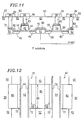
- Fig. 11 depicts transistors 38 and 40 of Fig. 10 following the deposition of a dielectric interlevel 82.
- Dielectric interlevel 82 has a top surface 83, and overlies source/drain areas 46, 48, 58, and 60.
- Dielectric interlevel 82 also overlies surrounding the field oxide regions 50, 52, and 62.
- Contact holes 84 are patterned through dielectric interlevel 82 from dielectric inner level surface 83 to silicide film 80 overlying selected adjoining areas of field oxide 50 and 62.
- Metal 86 is deposited in contact holes 84 to form electrical interconnects from dielectric interlevel surface 83, with silicide film 80, to source/drain regions 77.
- Fig. 12 is a plan view of transistors 38 and 40 of Fig. 10. The plan view is presented to highlight a strap interconnection between first 38 and sesond 40 CMOS transistors.
- the field oxide region 52 intervenes between first electrode 58 of second transistor 40, such as a source, and second electrode 48 of first transistor 38, such as a drain. Cut-outs through silicide film 80 show underlying electrodes 48 and 58.
- the method is applicable to connect a source, drain, or gate electrode of a transistor to the source, drain, or gate electrode of any other transistor. The method is especially useful in fabricating SRAM configurations to reduce cell size. At shown in Figs.
- silicide film 80 overlies first electrode 58 of second transistor 40 to second electrode 48 of first transistor 38 and selected areas of intervening field oxide region 52. That is, silicide film 80 overlies first electrode 58, through selected areas of intervening field oxide region 52, to said second electrode 48.
- Silicide film 80 is formed by depositing a layer semiconductor film 72 over transistors 38 and 40 and intervening field oxide region 52. Then, insulating layer 74 is deposited over semiconductor film 72 and anisotropically etched to form second gate electrode sidewalls 76. A refractory metal layer 78 overlies transistors 38 and 40, and selected areas of intervening field oxide 52. Transistors 38 and 40 are annealed to form silicide film 80.
- Etching is performed to remove unreacted refractory metal 78, second sidewalls 76, and semiconductor film 72 overlying first oxide sidewalls 44 and 56. In this manner, electrical connections are made from first transistor 38 to second transistor 40 across intervening field oxide region 52.
- silicide film 80 has a width 90 that varies in different aspects of the invention.
- Fig. 12 depicts width 90 as being approximately equal to the width of source/drain areas 46, 48, 58, and 60.
- refractory metal 78 is deposited over selected areas of source/drain areas 46, 48, 58, and 60 to form a narrower width 90 (not shown).
- Strap interconnections are not limited to connection between the source of a first transistor and the drains of a second transistor. Connections, as described above, are made between any transistor active area to any other active area on the same metal level. Likewise, multiple transistors are connected in some aspects of the invention, and the present invention connection is also used in both strap and via connection combinations.
- Fig. 13 is a flowchart illustrating a method for forming CMOS interconnections through surrounding field oxide regions.
- the interconnection method is applicable to transistors selected from the group consisting of bulk silicon, silicon on insulator (SOI), and raised source/drain the transistors.
- Step 100 in provides at least a first transistor with source/drain regions.
- Step 102 deposits a semiconductor film overlying the transistor, including the source/drain regions of the transistor and the surrounding field oxide regions.
- Step 102 includes the semiconductor film being selected from the group consisting of polysilicon and silicon-germanium compounds Si x Ge 1-x .
- the (x) of Si x Ge 1-x is in the range between 0.5 and 0.9.
- Step 102 includes the semiconductor film having a thickness in the range between 50 and 200 nm.
- Step 104 deposits a refractory metal layer overlying the semiconductor film, covering the semiconductor film which has previously been deposited over the source/drain regions and selected adjoining areas of field oxide.
- the refractory metal is selected from the group consisting on Ti, Co, W, Pt, and Ni.
- Step 106 anneals the semiconductor film deposited in Step 102 and refractory metal deposited in Step 104 to form a silicide film overlying the source/drain regions and the selected adjoining areas of field oxide.
- the silicide layer has a thickness in the range between 40 and 200 nm, and a resistivity in the range between 2 and 10 ohms per square inch. Generally, a thicker silicide layer results in lower resistivity.
- Step 108 is a product, where an electrical interconnection is made between the source/drain regions from the surrounding field oxide region to minimize the size of the source/drain regions.
- a step proceeds step 102 of forming a gate electrode with an underlying gate oxide layer and first oxide sidewalls.
- step 104 includes depositing a semiconductor film overlying the gate electrode and first oxide sidewalls.
- Step 102a deposits a layer of insulator, selected from the group consisting of silicon oxide (oxide) and silicon nitride (nitride), overlying the semiconductor film.
- Step 102b anisotropically etches the insulator deposited in Step 102a to remove the insulator on the source/drain regions, gate electrode, and surrounding field oxide region, but not the gate electrode sidewalls. In this manner, second sidewalls are formed.
- Step 104 includes depositing a refractory metal layer overlying the gate electrode and second sidewalls.
- Step 106 includes annealing the transistor to form a silicide film overlying the transistor in the regions where the semiconductor film was exposed in Step 102b including the gate electrode, but not the second sidewalls.
- the first sidewalls, the second sidewalls of Step 102b, and the intervening semiconductor film deposited in Step 102 have a combined sidewall thickness.
- Step 102c (not shown) dopes and anneals the source/drain regions to form active source/drain regions with source/drain widths approximately twice as wide as the combined sidewall thickness overlying the source/drain regions.
- Step 106a removes unreacted refractory metal overlying the second sidewalls, the second sidewalls themselves, and the semiconductor film overlying the first oxide sidewalls.
- Step 106a includes using a buffered hydrofluoride (BHF) to etch the second gate electrode sidewalls.
- Step 106a includes using phosphoric acid to etch the second gate electrode sidewalls.
- a NH 3 OH:H 2 O 2 :H 2 O solution is used to remove the semiconductor film.
- Step 106b deposits a dielectric interlevel, with a top surface, overlying a transistor.
- Step 106c etches the dielectric interlevel to form contact boles from the dielectric interlevel top surface to the silicide film overlying the selected areas of field oxide.
- Step 106d deposits metal in the contact holes to form electrical interconnects from the surface of the dielectric interlevel to the source/drain regions. In this manner, an interconnection is made without regard to the size of the source/drain regions.
- Step 106 includes two annealing sub-steps (not shown).
- the first Sub-step includes annealing at a temperature in the range between 450 and 650 degrees C.
- the second Sub-step includes annealing at a temperature in the range between 700 and 900 degrees C.
- Fig. 14 is a flowchart illustrating a method of forming a strap interconnection between transistors across a field oxide region.
- Step 200 includes at least a second transistor with a first electrode, such as a source region, a first transistor with a second electrode, such as a drain, and a field oxide region which at least partially surrounds the two transistors.
- the method is not limited to connecting a source to a drain. The method is applicable to connect the source, drain, and gate electrodes of one transistor to the source, drain, and gate electrodes of any other transistor.
- Step 202 deposits semiconductor film over the transistors, including the first electrode of the second transistor, the second electrode of the first transistor, and surrounding field oxide regions.
- Step 204 deposits a refractory metal layer overlying the semiconductor film, including the semiconductor film that has previously been deposited on, and covers the first and second electrodes and selected areas of field oxide intervening between the two transistors. That is, a field oxide region intervening between the first electrode of the second transistor and the second electrode of the first transistor.
- Step 206 anneals the semiconductor film deposited in Step 202 and the refractory metal deposited in Step 204 to form a silicide film over the first electrode of the second transistor, the second electrode of the first transistor, and the selected areas of intervening field oxide.
- the product, Step 208 is an electrical connection made from the first transistor to the second transistor across the intervening field oxide. Alternately, a strap connection can be made to any active area of a first transistor to any active area of a second transistor. Further, a strap connection is made to more than two transistor active areas in some aspects of the invention.
- a silicide film is formed between a gate electrode of a first transistor and an electrode of a second transistor. Then, an area of gate electrode not adjoining the first transistor's source/drain regions is chosen for the connection. A second sidewall is not formed at this chosen connection site so that a silicide film is formed extending from the gate electrode, over the first sidewall, and across an adjoining field oxide region to the second transistor electrode.
- the interconnection is applicable to both strap and via type connections.
- the surface area of the source/drain regions are extended into neighboring field oxide regions by forming a silicide film from the source/drain regions to the field oxide. Interconnections on the same metal level, or to another metal level are made by an electrical contact to the silicide covered field oxide.
- the source/drain regions need only be large enough to accept the silicide film.
- Transistors with small source/drain regions have smaller drain leakage currents and less parasitic capacitance. Other variations and embodiments of the present invention will occur to those skilled in the art.
Landscapes
- Electrodes Of Semiconductors (AREA)
- Metal-Oxide And Bipolar Metal-Oxide Semiconductor Integrated Circuits (AREA)
- Insulated Gate Type Field-Effect Transistor (AREA)
- Thin Film Transistor (AREA)
Claims (18)
- Verfahren zum Ausbilden einer Zwischenverbindung mindestens eines ersten Transistors (38), welcher aufweist Source/Draingebiete (46, 48), Feldoxidgebiete (50, 52) und eine Gateelektrode (42), mit einer darunter liegenden Gateoxidschicht (64) und ersten Oxidseitenwänden (44) sowie darüberliegenden Bereichen der Source/Draingebiete, wobei die Zwischenverbindung zu einem Source/Draingebiet ausgebildet wird, um sich über einen benachbarten Bereich des Feldoxidgebietes zu erstrecken, und eine durch Annealen einer geschichteten Struktur einer refraktorischen Metallschicht (78) auf einer Halbleiterschicht (72) ausgebildete Silizidschicht aufweist,
dadurch gekennzeichnet, dass das Verfahren folgende Schritte aufweist:a) Abscheiden einer Halbleiterschicht (72), welche über dem Transistor liegt und welche die Source/Drain-Gebiete, die Gateelektrode, die ersten Oxidseitenwände und die Feldoxidgebiete aufweist,b) Abscheiden einer Isolatorschicht (74), welche über der Halbleiterschicht liegt,c) anisotropes Ätzen des im Schritt b) abgeschiedenen Isolators, um den Isolator auf den Source/Draingebieten, der Gateelektrode und den Feldoxidgebieten zu entfernen, aber nicht von den Gateelektrodenseitenwänden, wodurch zweite Seitenwände (76) ausgebildet werden,d) Abscheiden einer refraktorischen Metallschicht (78), welche über der Halbleiterschicht liegt, wobei die Source/Draingebiete und ausgewählte benachbarte Gebiete des Feldoxids bedeckt werden, unde) Annealen der im Schritt a) abgeschiedenen Halbleiterschicht und des im Schritt d) abgeschiedenen refraktorischen Metalls, um eine Silizidschicht (80) auszubilden, welche die Source/Draingebiete und die ausgewählten benachbarten Gebiete des Feldoxids überdeckt, wodurch elektrische Verbindungen zu den Source/Draingebieten von den Feldoxidgebieten ausgebildet werden, um die Größe der Source/Draingebiete zu minimieren. - Verfahren nach Anspruch 1,bei welchem Schritt d) das Abscheiden der refraktorischen Metallschicht aufweist, so dass diese über der Gateelektrode und den zweiten Seitenwänden liegt, undbei welchem Schritt e) aufweist das Annealen des Transistors, um die Silizidschicht auszubilden, so dass diese in Gebieten, wo im Schritt c) die Halbleiterschicht freigelegt wird, über dem Transistor liegt, wobei die Gateelektrode aber nicht die zweiten Seitenwände mit eingeschlossen sind.
- Verfahren nach Anspruch 2,
welche nach dem Schritt e) den Schritt aufweist:f) Entfernen des nicht reagierten refraktorischen Metalls (78), welches über den zweiten Seitenwänden (76) liegt, der zweiten Seitenwände selbst und der Halbleiterschicht, welche über den ersten Oxidseitenwänden liegt. - Verfahren nach Anspruch 3,
welches nach dem Schritt f) die weiteren Schritte aufweist:g) Abscheiden eines dielektrischen Zwischenniveaus (82), welche über dem Transistor liegt, mit einer oberen Oberfläche (83),h) Ätzen des dielektrischen Zwischenniveaus, um Kontaktlöcher (84) von der oberen Oberfläche des dielektrischen Zwischenniveaus zur über den ausgewählten Gebieten des Feldoxids liegenden Silizidschicht auszubilden, undi) Abscheiden eines Metalls (86) in die Kontaktlöcher, um elektrische Verbindungen auszubilden von der Oberfläche des dielektrischen Zwischenniveaus zu den Source/Draingebieten, wodurch eine Verbindung ausgebildet wird unabhängig von der Größe der Source/Draingebiete. - Verfahren nach einem der vorangehenden Ansprüche,
bei welchem im Schritt a) die Halbleiterschicht aus der Gruppe ausgewählt wird, welche gebildet wird von Polysilizium und SixGe1-x. - Verfahren nach Anspruch 5,
bei welchem (x) in SixGe1-x im Bereich von 0,5 bis 0,9 liegt. - Verfahren nach einem der vorangehenden Ansprüche,
bei welchem der Transistor ausgewählt wird aus der Gruppe, welche gebildet wird von Bulksilizium-, Siliziumauf-Isolator- (SOI) und Transistor mit angehobener Source/Drain. - Verfahren nach einem der vorangehenden Ansprüche,
bei welchem der Schritt A) aufweist das Abscheiden der Halbleiterschicht mit einer Schichtdicke im Bereich zwischen 50 und 200 Nanometern (nm). - Verfahren nach Anspruch 3,
bei welchem im Schritt b) der Isolator ausgewählt wird aus der Gruppe, welche gebildet wird von Oxid und Nitrid. - Verfahren nach Anspruch 9,bei welchem der Schritt b) das Abscheiden eines Oxidisolators aufweist undbei welchem im Schritt f) ein Ätzen mit gepuffertem Fluorwasserstoff (BHF) durchgeführt wird, um die zweiten Gateelektrodenoxidseitenwände zu entfernen, und wobei NH3OH:H2O2:H2O-Lösung verwendet wird, um die Halbleiterschicht zu entfernen.
- Verfahren nach Anspruch 9,bei welchem Schritt b) das Abscheiden eines Nitridisolators aufweist undbei welchem in Schritt f) Phosphorsäure zum Entfernen der zweiten Gateelektrodennitridseitenwände und NH3OH:H2O2:H2O-Lösung zum Entfernen der Halbleiterschicht verwendet werden.
- Verfahren nach einem der vorangehenden Ansprüche,
bei welchem in Schritt d) das refraktorische Metall aus der Gruppe gewählt wird, welche besteht aus Ti, Co, W, Pt und Ni. - Verfahren nach einem der vorangehenden Ansprüche,
bei welchem Schritt e) aufweist das Ausbilden der Silizidschicht derart, dass diese eine Stärke im Bereich von 40 bis 200 nm aufweist. - Verfahren nach einem der vorangehenden Ansprüche,
bei welchem der Schritt e) aufweist das Ausbilden der Silizidschicht derart, dass diese einen Widerstand im Bereich zwischen 2 und 10 Ohm pro Quadratzentimeter aufweist. - Verfahren nach einem der vorangehenden Ansprüche,
bei welchem der Schritt e) zwei Annealingunterschritte aufweist, wobei ein erster Annealingunterschritt aufweist das Annealen bei einer Temperatur im Bereich zwischen 450 und 650 Grad C und bei welchem der zweite Zwischenschritt aufweist das Annealen bei einer Temperatur im Bereich zwischen 700 und 900 Grad C. - Verfahren nach einem der vorangehenden Ansprüche,
bei welchem die ersten Seitenwände, die zweiten Seitenwände des Schritts c) und die im Schritt a) abgeschiedene dazwischenliegende Halbleiterschicht eine kombinierte Seitenwandstärke aufweisen und
welches nach dem Schritt c) den Schritt aufweist:c) Dotieren und Annealen der Source/Draingebiete, um aktive Source/Draingebiete mit Source/Drainbreiten auszubilden, welche ungefähr die zweifache Breite der kombinierten Seitenwandstärke sind, welche über den Source/Draingebieten liegt. - Verfahren zum Ausbilden einer Strapverbindung von mindestens einem ersten Transistor (38) mit Source/Drainelektroden (46, 48) zu einem zweiten Transistor (40) mit Source/Drainelektroden (48, 60) aufweist über einem dazwischenliegenden Feldoxidbereich (52), welcher die Transistoren trennt, wobei jeder der Transistoren des Weiteren eine Gateelektrode (42, 54) mit einer darunterliegenden Gateoxidschicht (64, 66) und mit ersten Oxidseitenwänden (44, 56) aufweist,
dadurch gekennzeichnet, dass das Verfahren Schritte aufweist:a) Abscheiden einer Halbleiterschicht (72), welche über den Transistoren liegt, wobei umfasst sind eine erste Elektrode (58) des zweiten Transistors, eine zweite Elektrode (48) des ersten Transistors, die ersten Oxidseitenwände sowie der dazwischenliegende Feldoxidbereich,b) Abscheiden einer Isolatorschicht (74), welche über der Halbleiterschicht liegt,c) anisotropes Ätzen des im Schritt b) abgeschiedenen Isolators, um den Isolator auf den ersten und zweiten Elektroden, auf dem Feldoxidbereich, aber nicht von den zweiten Gateelektrodenseitenwänden zu entfernen, wodurch zweite Seitenwände (76) ausgebildet werden,d) Abscheiden einer refraktorischen Metallschicht (78), welche über der Halbleiterschicht liegt, wobei die ersten und zweiten Elektroden (58, 48) und ausgewählte Bereiche des dazwischen liegenden Feldoxids (52) abgedeckt werden, unde) Annealen der im Schritt a) abgeschiedenen Halbleiterschicht und des im Schritt d) abgeschiedenen refraktorischen Metalls, um eine Silizidschicht (80) auszubilden, welche über der ersten Elektrode des zweiten Transistors, der zweiten Elektrode des ersten Transistors und den ausgewählten Bereichen des dazwischen liegenden Feldoxids liegt, wodurch eine elektrische Verbindung ausgebildet wird vom ersten Transistor zum zweiten Transistor über dem dazwischenliegenden Feldoxid. - Verfahren nach Anspruch 17,
bei welchem die ersten und zweiten Elektroden aus der Gruppe ausgewählt werden, welche gebildet wird von Source- und Drainelektroden.
Applications Claiming Priority (2)
| Application Number | Priority Date | Filing Date | Title |
|---|---|---|---|
| US90802 | 1987-08-28 | ||
| US09/090,802 US5915199A (en) | 1998-06-04 | 1998-06-04 | Method for manufacturing a CMOS self-aligned strapped interconnection |
Publications (2)
| Publication Number | Publication Date |
|---|---|
| EP0964447A1 EP0964447A1 (de) | 1999-12-15 |
| EP0964447B1 true EP0964447B1 (de) | 2002-06-05 |
Family
ID=22224388
Family Applications (1)
| Application Number | Title | Priority Date | Filing Date |
|---|---|---|---|
| EP99301698A Expired - Lifetime EP0964447B1 (de) | 1998-06-04 | 1999-03-08 | Herstellungsverfahren für selbstjustierende lokale Zwischenverbindung |
Country Status (6)
| Country | Link |
|---|---|
| US (2) | US5915199A (de) |
| EP (1) | EP0964447B1 (de) |
| JP (1) | JP3860672B2 (de) |
| KR (1) | KR100375752B1 (de) |
| DE (1) | DE69901657T2 (de) |
| TW (1) | TW465067B (de) |
Families Citing this family (43)
| Publication number | Priority date | Publication date | Assignee | Title |
|---|---|---|---|---|
| US6001697A (en) * | 1998-03-24 | 1999-12-14 | Mosel Vitelic Inc. | Process for manufacturing semiconductor devices having raised doped regions |
| US5915199A (en) * | 1998-06-04 | 1999-06-22 | Sharp Microelectronics Technology, Inc. | Method for manufacturing a CMOS self-aligned strapped interconnection |
| US6399487B1 (en) * | 1998-12-28 | 2002-06-04 | Taiwan Semiconductor Manufacturing Company | Method of reducing phase transition temperature by using silicon-germanium alloys |
| US6274409B1 (en) * | 2000-01-18 | 2001-08-14 | Agere Systems Guardian Corp. | Method for making a semiconductor device |
| US6403485B1 (en) * | 2001-05-02 | 2002-06-11 | Chartered Semiconductor Manufacturing Ltd | Method to form a low parasitic capacitance pseudo-SOI CMOS device |
| US6534807B2 (en) * | 2001-08-13 | 2003-03-18 | International Business Machines Corporation | Local interconnect junction on insulator (JOI) structure |
| US6727168B2 (en) * | 2001-10-24 | 2004-04-27 | Micron Technology, Inc. | Method of forming local interconnects |
| JP2004047608A (ja) * | 2002-07-10 | 2004-02-12 | Toshiba Corp | 半導体装置及びその製造方法 |
| KR100845719B1 (ko) * | 2002-12-28 | 2008-07-10 | 동부일렉트로닉스 주식회사 | 반도체 소자 및 그 제조방법 |
| FR2856843A1 (fr) * | 2003-06-25 | 2004-12-31 | St Microelectronics Sa | Procede de protection d'un element d'un circuit integre contre la formation d'un siliciure de metal |
| US7078259B2 (en) * | 2004-01-08 | 2006-07-18 | International Business Machines Corporation | Method for integrating thermistor |
| US7566609B2 (en) * | 2005-11-29 | 2009-07-28 | International Business Machines Corporation | Method of manufacturing a semiconductor structure |
| US8247846B2 (en) | 2006-03-09 | 2012-08-21 | Tela Innovations, Inc. | Oversized contacts and vias in semiconductor chip defined by linearly constrained topology |
| US9230910B2 (en) | 2006-03-09 | 2016-01-05 | Tela Innovations, Inc. | Oversized contacts and vias in layout defined by linearly constrained topology |
| US9009641B2 (en) | 2006-03-09 | 2015-04-14 | Tela Innovations, Inc. | Circuits with linear finfet structures |
| US7763534B2 (en) * | 2007-10-26 | 2010-07-27 | Tela Innovations, Inc. | Methods, structures and designs for self-aligning local interconnects used in integrated circuits |
| US8245180B2 (en) | 2006-03-09 | 2012-08-14 | Tela Innovations, Inc. | Methods for defining and using co-optimized nanopatterns for integrated circuit design and apparatus implementing same |
| US9035359B2 (en) | 2006-03-09 | 2015-05-19 | Tela Innovations, Inc. | Semiconductor chip including region including linear-shaped conductive structures forming gate electrodes and having electrical connection areas arranged relative to inner region between transistors of different types and associated methods |
| US8448102B2 (en) | 2006-03-09 | 2013-05-21 | Tela Innovations, Inc. | Optimizing layout of irregular structures in regular layout context |
| US8225261B2 (en) | 2006-03-09 | 2012-07-17 | Tela Innovations, Inc. | Methods for defining contact grid in dynamic array architecture |
| US8658542B2 (en) | 2006-03-09 | 2014-02-25 | Tela Innovations, Inc. | Coarse grid design methods and structures |
| US7943967B2 (en) * | 2006-03-09 | 2011-05-17 | Tela Innovations, Inc. | Semiconductor device and associated layouts including diffusion contact placement restriction based on relation to linear conductive segments |
| US8653857B2 (en) | 2006-03-09 | 2014-02-18 | Tela Innovations, Inc. | Circuitry and layouts for XOR and XNOR logic |
| US7446352B2 (en) | 2006-03-09 | 2008-11-04 | Tela Innovations, Inc. | Dynamic array architecture |
| US8225239B2 (en) | 2006-03-09 | 2012-07-17 | Tela Innovations, Inc. | Methods for defining and utilizing sub-resolution features in linear topology |
| US7917879B2 (en) | 2007-08-02 | 2011-03-29 | Tela Innovations, Inc. | Semiconductor device with dynamic array section |
| US7956421B2 (en) | 2008-03-13 | 2011-06-07 | Tela Innovations, Inc. | Cross-coupled transistor layouts in restricted gate level layout architecture |
| US8839175B2 (en) | 2006-03-09 | 2014-09-16 | Tela Innovations, Inc. | Scalable meta-data objects |
| US7932545B2 (en) | 2006-03-09 | 2011-04-26 | Tela Innovations, Inc. | Semiconductor device and associated layouts including gate electrode level region having arrangement of six linear conductive segments with side-to-side spacing less than 360 nanometers |
| US9563733B2 (en) | 2009-05-06 | 2017-02-07 | Tela Innovations, Inc. | Cell circuit and layout with linear finfet structures |
| US8541879B2 (en) | 2007-12-13 | 2013-09-24 | Tela Innovations, Inc. | Super-self-aligned contacts and method for making the same |
| US7979829B2 (en) | 2007-02-20 | 2011-07-12 | Tela Innovations, Inc. | Integrated circuit cell library with cell-level process compensation technique (PCT) application and associated methods |
| US8286107B2 (en) | 2007-02-20 | 2012-10-09 | Tela Innovations, Inc. | Methods and systems for process compensation technique acceleration |
| US8667443B2 (en) | 2007-03-05 | 2014-03-04 | Tela Innovations, Inc. | Integrated circuit cell library for multiple patterning |
| US20090050975A1 (en) * | 2007-08-21 | 2009-02-26 | Andres Bryant | Active Silicon Interconnect in Merged Finfet Process |
| US8453094B2 (en) | 2008-01-31 | 2013-05-28 | Tela Innovations, Inc. | Enforcement of semiconductor structure regularity for localized transistors and interconnect |
| US7939443B2 (en) | 2008-03-27 | 2011-05-10 | Tela Innovations, Inc. | Methods for multi-wire routing and apparatus implementing same |
| KR101903975B1 (ko) | 2008-07-16 | 2018-10-04 | 텔라 이노베이션스, 인코포레이티드 | 동적 어레이 아키텍쳐에서의 셀 페이징과 배치를 위한 방법 및 그 구현 |
| US9122832B2 (en) | 2008-08-01 | 2015-09-01 | Tela Innovations, Inc. | Methods for controlling microloading variation in semiconductor wafer layout and fabrication |
| US8507996B2 (en) * | 2009-09-22 | 2013-08-13 | Taiwan Semiconductor Manufacturing Company, Ltd. | Block contact plugs for MOS devices |
| US8661392B2 (en) | 2009-10-13 | 2014-02-25 | Tela Innovations, Inc. | Methods for cell boundary encroachment and layouts implementing the Same |
| US9159627B2 (en) | 2010-11-12 | 2015-10-13 | Tela Innovations, Inc. | Methods for linewidth modification and apparatus implementing the same |
| US10692808B2 (en) | 2017-09-18 | 2020-06-23 | Qualcomm Incorporated | High performance cell design in a technology with high density metal routing |
Family Cites Families (20)
| Publication number | Priority date | Publication date | Assignee | Title |
|---|---|---|---|---|
| NL8202777A (nl) * | 1982-07-09 | 1984-02-01 | Philips Nv | Halfgeleiderinrichting en werkwijze voor het vervaardigen daarvan. |
| US4592927A (en) * | 1982-09-24 | 1986-06-03 | At&T Bell Laboratories | Growth of oxide thin films using solid oxygen sources |
| US4873204A (en) * | 1984-06-15 | 1989-10-10 | Hewlett-Packard Company | Method for making silicide interconnection structures for integrated circuit devices |
| US5121186A (en) * | 1984-06-15 | 1992-06-09 | Hewlett-Packard Company | Integrated circuit device having improved junction connections |
| JPS61139058A (ja) * | 1984-12-11 | 1986-06-26 | Seiko Epson Corp | 半導体製造装置 |
| JPH01231376A (ja) * | 1988-03-11 | 1989-09-14 | Nec Corp | 薄膜トランジスタおよびその製造方法 |
| US5418179A (en) * | 1988-05-31 | 1995-05-23 | Yamaha Corporation | Process of fabricating complementary inverter circuit having multi-level interconnection |
| US5294822A (en) * | 1989-07-10 | 1994-03-15 | Texas Instruments Incorporated | Polycide local interconnect method and structure |
| US5156994A (en) * | 1990-12-21 | 1992-10-20 | Texas Instruments Incorporated | Local interconnect method and structure |
| JP2994128B2 (ja) * | 1991-03-04 | 1999-12-27 | シャープ株式会社 | 半導体装置の製造方法 |
| US5250467A (en) * | 1991-03-29 | 1993-10-05 | Applied Materials, Inc. | Method for forming low resistance and low defect density tungsten contacts to silicon semiconductor wafer |
| JP2675713B2 (ja) * | 1991-05-10 | 1997-11-12 | 株式会社東芝 | 半導体装置及びその製造方法 |
| US5242847A (en) * | 1992-07-27 | 1993-09-07 | North Carolina State University At Raleigh | Selective deposition of doped silion-germanium alloy on semiconductor substrate |
| EP0622834A3 (de) * | 1993-04-30 | 1998-02-11 | International Business Machines Corporation | Verfahren zur Latch-up Vermeidung und Durchbruchspannung Verbesserung in SOI MOSFET |
| JPH06333944A (ja) * | 1993-05-25 | 1994-12-02 | Nippondenso Co Ltd | 半導体装置 |
| US5635426A (en) * | 1993-08-26 | 1997-06-03 | Fujitsu Limited | Method of making a semiconductor device having a silicide local interconnect |
| US5567966A (en) * | 1993-09-29 | 1996-10-22 | Texas Instruments Incorporated | Local thinning of channel region for ultra-thin film SOI MOSFET with elevated source/drain |
| JP2551353B2 (ja) * | 1993-10-07 | 1996-11-06 | 日本電気株式会社 | 半導体装置及びその製造方法 |
| SG47355A1 (en) * | 1994-09-01 | 1998-04-17 | Two Yeow Meng | Local interconnects and method for making electrical local interconnects |
| US5915199A (en) * | 1998-06-04 | 1999-06-22 | Sharp Microelectronics Technology, Inc. | Method for manufacturing a CMOS self-aligned strapped interconnection |
-
1998
- 1998-06-04 US US09/090,802 patent/US5915199A/en not_active Expired - Fee Related
-
1999
- 1999-02-17 JP JP03925899A patent/JP3860672B2/ja not_active Expired - Fee Related
- 1999-02-24 TW TW088102745A patent/TW465067B/zh not_active IP Right Cessation
- 1999-02-25 US US09/257,217 patent/US6388296B1/en not_active Expired - Fee Related
- 1999-03-08 DE DE69901657T patent/DE69901657T2/de not_active Expired - Fee Related
- 1999-03-08 EP EP99301698A patent/EP0964447B1/de not_active Expired - Lifetime
- 1999-05-14 KR KR10-1999-0017339A patent/KR100375752B1/ko not_active Expired - Fee Related
Also Published As
| Publication number | Publication date |
|---|---|
| KR20000005660A (ko) | 2000-01-25 |
| DE69901657T2 (de) | 2003-02-06 |
| DE69901657D1 (de) | 2002-07-11 |
| US6388296B1 (en) | 2002-05-14 |
| TW465067B (en) | 2001-11-21 |
| EP0964447A1 (de) | 1999-12-15 |
| KR100375752B1 (ko) | 2003-03-15 |
| JPH11354651A (ja) | 1999-12-24 |
| US5915199A (en) | 1999-06-22 |
| JP3860672B2 (ja) | 2006-12-20 |
Similar Documents
| Publication | Publication Date | Title |
|---|---|---|
| US5915199A (en) | Method for manufacturing a CMOS self-aligned strapped interconnection | |
| US7045409B2 (en) | Semiconductor device having active regions connected together by interconnect layer and method of manufacture thereof | |
| US5241193A (en) | Semiconductor device having a thin-film transistor and process | |
| US5777370A (en) | Trench isolation of field effect transistors | |
| US5538913A (en) | Process for fabricating MOS transistors having full-overlap lightly-doped drain structure | |
| US6737308B2 (en) | Semiconductor device having LDD-type source/drain regions and fabrication method thereof | |
| US6573583B2 (en) | Semiconductor device and method of manufacturing the same | |
| EP0334761B1 (de) | Verfahren zum Herstellen eines selbstisolierenden source/drain-Kontaktes in einem MOS-Transistor | |
| EP0088922B1 (de) | Verfahren zum Herstellen von Elektroden und Verdrahtungsstreifen auf einer Halbleiteranordnung | |
| US7338873B2 (en) | Method of fabricating a field effect transistor structure with abrupt source/drain junctions | |
| US5804846A (en) | Process for forming a self-aligned raised source/drain MOS device and device therefrom | |
| US6608354B2 (en) | Semiconductor device and method of manufacturing the same | |
| US5612240A (en) | Method for making electrical connections to self-aligned contacts that extends beyond the photo-lithographic resolution limit | |
| US20040175919A1 (en) | Borderless contact structure and method of forming the same | |
| US20010002058A1 (en) | Semiconductor apparatus and method of manufacture | |
| US5213990A (en) | Method for forming a stacked semiconductor structure | |
| US6300172B1 (en) | Method of field isolation in silicon-on-insulator technology | |
| US5898189A (en) | Integrated circuit including an oxide-isolated localized substrate and a standard silicon substrate and fabrication method | |
| US5986312A (en) | Field effect semiconductor device having improved connections | |
| US6287911B1 (en) | Semiconductor device with silicide layers and fabrication method thereof | |
| US5731240A (en) | Manufacturing method for semiconductor depositing device | |
| US5926706A (en) | Method for making a trench-free buried contact with low resistance on semiconductor integrated circuits | |
| US5926728A (en) | Method for fabricating tungsten polycide contacts | |
| US7169676B1 (en) | Semiconductor devices and methods for forming the same including contacting gate to source | |
| US7029963B2 (en) | Semiconductor damascene trench and methods thereof |
Legal Events
| Date | Code | Title | Description |
|---|---|---|---|
| PUAI | Public reference made under article 153(3) epc to a published international application that has entered the european phase |
Free format text: ORIGINAL CODE: 0009012 |
|
| AK | Designated contracting states |
Kind code of ref document: A1 Designated state(s): DE FR GB |
|
| AX | Request for extension of the european patent |
Free format text: AL;LT;LV;MK;RO;SI |
|
| 17P | Request for examination filed |
Effective date: 20000601 |
|
| AKX | Designation fees paid |
Free format text: DE FR GB |
|
| 17Q | First examination report despatched |
Effective date: 20001016 |
|
| GRAG | Despatch of communication of intention to grant |
Free format text: ORIGINAL CODE: EPIDOS AGRA |
|
| RTI1 | Title (correction) |
Free format text: MANUFACTURING METHOD FOR SELF-ALIGNED LOCAL INTERCONNECTION FOR CMOS |
|
| GRAG | Despatch of communication of intention to grant |
Free format text: ORIGINAL CODE: EPIDOS AGRA |
|
| GRAH | Despatch of communication of intention to grant a patent |
Free format text: ORIGINAL CODE: EPIDOS IGRA |
|
| GRAH | Despatch of communication of intention to grant a patent |
Free format text: ORIGINAL CODE: EPIDOS IGRA |
|
| GRAA | (expected) grant |
Free format text: ORIGINAL CODE: 0009210 |
|
| AK | Designated contracting states |
Kind code of ref document: B1 Designated state(s): DE FR GB |
|
| REG | Reference to a national code |
Ref country code: GB Ref legal event code: FG4D |
|
| REF | Corresponds to: |
Ref document number: 69901657 Country of ref document: DE Date of ref document: 20020711 |
|
| ET | Fr: translation filed | ||
| PLBE | No opposition filed within time limit |
Free format text: ORIGINAL CODE: 0009261 |
|
| STAA | Information on the status of an ep patent application or granted ep patent |
Free format text: STATUS: NO OPPOSITION FILED WITHIN TIME LIMIT |
|
| 26N | No opposition filed |
Effective date: 20030306 |
|
| PGFP | Annual fee paid to national office [announced via postgrant information from national office to epo] |
Ref country code: GB Payment date: 20090304 Year of fee payment: 11 |
|
| PGFP | Annual fee paid to national office [announced via postgrant information from national office to epo] |
Ref country code: DE Payment date: 20090306 Year of fee payment: 11 |
|
| PGFP | Annual fee paid to national office [announced via postgrant information from national office to epo] |
Ref country code: FR Payment date: 20090316 Year of fee payment: 11 |
|
| GBPC | Gb: european patent ceased through non-payment of renewal fee |
Effective date: 20100308 |
|
| REG | Reference to a national code |
Ref country code: FR Ref legal event code: ST Effective date: 20101130 |
|
| PG25 | Lapsed in a contracting state [announced via postgrant information from national office to epo] |
Ref country code: FR Free format text: LAPSE BECAUSE OF NON-PAYMENT OF DUE FEES Effective date: 20100331 |
|
| PG25 | Lapsed in a contracting state [announced via postgrant information from national office to epo] |
Ref country code: DE Free format text: LAPSE BECAUSE OF NON-PAYMENT OF DUE FEES Effective date: 20101001 |
|
| PG25 | Lapsed in a contracting state [announced via postgrant information from national office to epo] |
Ref country code: GB Free format text: LAPSE BECAUSE OF NON-PAYMENT OF DUE FEES Effective date: 20100308 |