EP0965172B1 - Dispositif de codage/decodage de mots source de n bits en mots canal correspondants de m bits, et vice versa - Google Patents
Dispositif de codage/decodage de mots source de n bits en mots canal correspondants de m bits, et vice versa Download PDFInfo
- Publication number
- EP0965172B1 EP0965172B1 EP99900067A EP99900067A EP0965172B1 EP 0965172 B1 EP0965172 B1 EP 0965172B1 EP 99900067 A EP99900067 A EP 99900067A EP 99900067 A EP99900067 A EP 99900067A EP 0965172 B1 EP0965172 B1 EP 0965172B1
- Authority
- EP
- European Patent Office
- Prior art keywords
- bit
- words
- signal
- consecutive
- channel
- Prior art date
- Legal status (The legal status is an assumption and is not a legal conclusion. Google has not performed a legal analysis and makes no representation as to the accuracy of the status listed.)
- Expired - Lifetime
Links
- 239000002131 composite material Substances 0.000 claims abstract description 128
- 238000006243 chemical reaction Methods 0.000 claims abstract description 51
- 238000001514 detection method Methods 0.000 claims description 19
- 230000004044 response Effects 0.000 claims description 18
- 230000003287 optical effect Effects 0.000 claims description 9
- 238000012217 deletion Methods 0.000 claims description 6
- 230000037430 deletion Effects 0.000 claims description 6
- 238000000034 method Methods 0.000 claims description 4
- 230000007704 transition Effects 0.000 description 6
- 230000006870 function Effects 0.000 description 4
- 238000003780 insertion Methods 0.000 description 4
- 230000037431 insertion Effects 0.000 description 4
- 230000004048 modification Effects 0.000 description 4
- 238000012986 modification Methods 0.000 description 4
- 230000005540 biological transmission Effects 0.000 description 3
- 230000008569 process Effects 0.000 description 1
- 238000012545 processing Methods 0.000 description 1
Images




Classifications
-
- H—ELECTRICITY
- H03—ELECTRONIC CIRCUITRY
- H03M—CODING; DECODING; CODE CONVERSION IN GENERAL
- H03M7/00—Conversion of a code where information is represented by a given sequence or number of digits to a code where the same, similar or subset of information is represented by a different sequence or number of digits
-
- H—ELECTRICITY
- H03—ELECTRONIC CIRCUITRY
- H03M—CODING; DECODING; CODE CONVERSION IN GENERAL
- H03M5/00—Conversion of the form of the representation of individual digits
- H03M5/02—Conversion to or from representation by pulses
- H03M5/04—Conversion to or from representation by pulses the pulses having two levels
- H03M5/14—Code representation, e.g. transition, for a given bit cell depending on the information in one or more adjacent bit cells, e.g. delay modulation code, double density code
- H03M5/145—Conversion to or from block codes or representations thereof
-
- H—ELECTRICITY
- H03—ELECTRONIC CIRCUITRY
- H03M—CODING; DECODING; CODE CONVERSION IN GENERAL
- H03M7/00—Conversion of a code where information is represented by a given sequence or number of digits to a code where the same, similar or subset of information is represented by a different sequence or number of digits
- H03M7/14—Conversion to or from non-weighted codes
- H03M7/20—Conversion to or from n-out-of-m codes
Definitions
- the invention relates to a device for encoding a stream of databits of binary source signal into a stream of databits of a binary channel signal, the binary source signal comprising a sequence of consecutive n-hit source words and the binary channel signal comprising a sequence of consecutive m-bit channel words, the device comprising
- the invention overcomes this error propagation, in that by shifting q bits in each second group of y consecutive bits source words in the binary source signal, the boundaries between two subsequent n-bit source words of the binary source signal are aligned with the boundaries between two subsequent n-bit words in the composite binary source signal. As a result, no error propagation will occur.
- the merging means therefore influences the output signal of the 1T precoder such that the running digital sum value of the output signal of the 1T precoder can be controlled so as to have a desired pattern as a function of time.
- FIG. 1 shows an embodiment of the encoding device in accordance with the invention.
- the device comprises an input terminal 1 for receiving a binary source signal, which terminal is coupled to an input 2 of a q-bit word merging unit 4.
- An output 6 of the unit 4 is coupled to an input 7 of a shuffling unit 8.
- the shuffling unit 8 has an output 9 which is coupled to an input 11 of a converter unit 10, which has an output 12 which is coupled to an input 14 of an aT precoder 16.
- An output 18 of the precoder 16 is coupled to an output for supplying a binary channel signal.
- the output 18 is also coupled to an input 22 of a control signal generator 24, which has an output 26 coupled to a control signal input 28 of the merging unit 4.
- a binary source signal, in the form of a sequence of n-bit source words is applied to the input terminal 1 for encoding.
- the merging unit 4 is adapted to insert a q-bit merging word at equidistant positions in the binary source signal. More specifically, the merging unit 4 is adapted to insert a q-bit merging word each time between subsequent groups of x consecutive n-bit source words in the binary source signal so as to obtain a composite binary source signal at its output 6.
- the binary channel signal is subsequently precoded into a precoded binary channel signal in the aT precoder 16 and the precoded binary channel signal is subsequently supplied to the output terminal 20, eg. for recording or transmission, as well as to the input 22 of the control signal generator 24.
- the control signal generator 24 generates a control signal at its output 26 in response to said precoded binary channel signal, which control signal is supplied to the control signal input 28 of the merging unit 4.
- the merging unit 4 chooses a q-bit word in response to said control signal for merging into the binary source signal.
- x could have any integer value. In an example to be described later, x will be equal to 24, for the reason that a 1-bit merging word is inserted between subsequent groups of 6 bytes of the binary source signal.
- the converter unit 10' is adapted to generate a (d,k) sequence as explained above, it causes the output signal of the device of figure 1 or 2 to be a (d,k) RLL output signal.
- Embodiments of the merging unit 4 are given in Bell System Technical Journal, Vol 53, No. 6, pp. 1103-1106.
- Figure 3 shows in figure 3a schematically the binary source signal applied to the input terminal 1 of the device.
- the source signal comprises a sequence of 2-bit source words, denoted sw 1 , sw 2 , .... sw i , sw i+1 , ...
- 2-bit source words of the binary source signal form a byte in the binary source signal. Sequence of each time six consecutive bytes B 0 , ... B 5 are shown in figure 3a.
- the merging unit 4' of figure 2 is adapted to insert a 1-bit merging word each time between those groups of six consecutive bytes B 0 to B 5 in the binary source signal, that is: a 1-bit merging word is each time inserted between subsequent groups of 24 2-bit source words of the binary source signal.
- a merging word mw o is merged between the source words sw 2 and sw 3 of the binary source signal and a merging word mw 1 is merged between the source words sw i+3 and sw i+4 , resulting into the composite source signal shown in figure 3b.
- FIG. 3c shows the composite source signal divided into a sequence of 2-bit words, the so-called composite source words, denoted csw 1 , csw 2 , csw 3 ,.... Those composite source words are converted into corresponding 3-bit channel words, resulting in the channel signal shown schematically in figure 3d.
- the channel words in the channel signal are denoted cw i .
- Figure 3d shows the channel words cw 2 , cw 7 , cw 11 and cw i , obtained from converting the 2-bit composite source words csw 2 , csw 7 , csw 11 and csw i , respectively.
- the 3-bit channel words are reconverted into replicas of the original 2-bit composite source words.
- figure 3e shows the sequence of the replicas of the composite source words, denoted rcsw 1 , rcsw 2 , rcsw 3 , ...., rcsw i .
- the merging words mw 0 and mw 1 included in the replicas rcsw 3 and rcsw i+4 are deleted from those replicas, resulting in the replica of the original source signal, shown schematically in figure 3f.
- Figure 3f shows the replica of the source signal, in the form of a sequence of replicas of the original source words, those replicas being denoted in figure 3f by rsw 1 , rsw 2 , rsw 3 , ...., rsw i , rsw i+1 , ....
- the first bit of the word rcsw 7 is the seventh bit b 7 of the byte B 0 and the second bit in the word rcsw 7 is the first bit b 0 of the byte B 1 in the replica of the source signal of figure 3f.
- the word rcsw 7 is erroneous, so are the bytes B 0 and B 1 .
- error propagation occurs, as an error in one word of the replica of the composite source signal results in an error in two bytes of the replica of the source signal.
- a shuffling step is carried out on the composite source signal, prior to supplying the composite source signal to the converter unit 10'.
- Figure 4 shows one embodiment of this shuffling step and figure 5 shows another embodiment.
- Figure 4a shows again the serial datastream of the binary source signal, in which a 1-bit merging word is inserted each time between subsequent groups of 24 2-bit source words.
- Figure 4b shows again how a merging word mw 0 is inserted after the source word sw 2 and a merging word mw 1 is inserted before the source word sw i+4 .
- a shuffling step is carried out on the signal obtained after merging the merging words.
- the result of the merging and shuffling step is shown by the signal of figure 4b, which shows the shuffled composite signal in the form of 2-bit words w 1 , w 2 , .... w i , w i+1 , «
- the sequence of 2-bit source words following the source word sw 2 is shifted to the right in figure 4b over an additonal bit position, resulting in an empty bit position between the merging word mw 0 and the word w 4 of the shuffled signal.
- the word w 4 in the shuffled signal equals the source word sw 3
- the word w 5 in the shuffled signal equals the source word sw 4
- the word w i+3 which equals the source word sw i+2
- the last two bits of the byte B 5 , the bits b 6 and b 7 are included in the source word sw i+3 .
- the bit b 6 directly follows the word w i+3 , as can be seen in figure 4b.
- the bit b 7 is repositioned and placed into the empty bit position between the merging word mw 0 and the word w 4 . This is indicated in figure 4b by the arrow 50.
- the next merging word mw 1 is inserted as the second bit of the 2-bit word w i+4 , which is followed by the 2-bit word sw i+5 which equals the source word sw i+4 , and so on. It is clear from figure 4a and 4b that the boundaries between the words in the shuffled composite signal of figure 4b now coincide with the boundaries of the source words in the source signal of figure 4a.
- Converting the 2-bit words of the shuffled composite signal into 3-bit channel words leads to the channel signal of figure 4c. Subsequent reconversion leads to a replica of the shuffled composite signal which is shown in figure 4d.
- the merging words are deleted from the replica of the shuffled composite signal. That means: the first bit of the replica of the word rw 3 is deleted and the second bit of the word rw i+4 is deleted. Further, the second bit of the word rw 3 is retrieved from the serial datastream, so that the word rsw 3 that follows the word rsw 2 of the replica of the source signal equals the 2-bit word rw 4 of the replica of the shuffled composite signal, and so on.
- the word rsw i+2 of the replica of the source signal equals the word rw i+3 of the replica of the shuffled composite signal and the word rsw i+4 equals the word rw i+5 .
- the bit b 6 of the byte B 5 of the replica of the source signal equals the first bit of the word rw i+4 of the replica of the shuffled composite signal.
- Deleting the merging word mw 1 means an empty bit position, which is filled in by the bit value of the second bit of the word rw 3 , giving the bit b 7 of the byte B 5 . This repositioning of the bit b 7 is shown in figure 4e by the arrow 52.
- An error occurring during the conversion/reconversion step results in an erroneous word rw i in the replica of the shuffled composite signal of figure 4d.
- rw i in the replica of the shuffled composite signal of figure 4d As the boundaries between the words rw i in the signal of figure 4d and the words rsw i in the signal of figure 4e are aligned, such error results in only one 2-bit word, and thus only one byte, to be erroneous, so that no error propagation occurs.
- Figure 5 shows another way of shuffling the composite source signal.
- Figure 5a shows again the serial datastream of the binary source signal.
- Figure 5b shows again how a merging word mw 0 is inserted after the source word sw 2 and a merging word mw 1 is inserted before the source word sw i+4 .
- the shuffling step now comprises repositioning the bit b 0 of the byte B 0 , that is: the first bit of the word sw 3 .
- the result of the merging and shuffling step is shown by the signal of figure 5b, which shows the shuffled composite signal in the form of 2-bit words w 1 , w 2 , .... w i , w i+1 , «
- the insertion of the merging word mw 0 in fact means a replacement of the bit b 0 of the byte B 0 by the merging word mw 0 , whilst the bit b 0 is temporarily stored.
- the word sw 4 in the source signal equals the word w 4 in the shuffled composite signal, and so on.
- the word sw i+3 of the source signal equals the word w i+3 of the shuffled composite signal.
- bit b 0 that was temporarily stored, is now added as the first bit of the word w i+4 and is followed by the merging word mw 1 as the second bit of the word w i+4 .
- This is schematically shown by the arrow 54 in figure 5b.
- the following source words sw i+4 , sw i+5 , .... are shifted over two bit positions. But in all cases, the boundaries between the 2-bit words w in the shuffled composite signal of figure 5b and the source words sw in the source signal of figure 5a are aligned.
- the word rsw 4 that follows the word rsw 3 of the replica of the source signal equals the 2-bit word rw 4 of the replica of the shuffled composite signal, and so on.
- the word rsw i+3 of the replica of the source signal equals the word rw i+3 of the replica of the shuffled composite signal.
- the first bit of the word rw i+4 was already repositioned into the first bit position of the word rsw 3 .
- deleting the merging word mw 1 means that the words rw i+5 (and so on) directly follow the word rsw i+3 as the words rsw i+4 (and so on) of the replica of the source signal.
- the repositioning of the bit b 0 is shown in figure 5e by the arrow 56.
- An error occurring during the conversion/reconversion step results in an erroneous word rw i in the replica of the shuffled composite signal of figure 5d.
- rw i in the replica of the shuffled composite signal of figure 5d As the boundaries between the words rw i in the signal of figure 5d and the words rsw i in the signal of figure 5e are aligned, such error results in only one 2-bit word, and thus only one byte, to be erroneous, so that no error propagation occurs.
- shuffling step has been described as a step that follows the merging step. It should however be noted that the shuffling step could precede the merging step, or could coincide with the merging step.
- FIG. 6 shows an embodiment of the shuffling unit 8' for carrying out the shuffling step described with reference to the figures 4a and 4b.
- the shuffling unit of figure 6 comprises a memory in the form of a shift register 40 having, in the example given, 47 storage locations. Further first and second controllable switches 42 and 44 are available having terminals a, b and c. Further, a control unit CPU is available for controlling the positions of the switches 42 and 44 via a control line 46 and for controlling the shifting of the information through the shift register 40 via a control line 48.
- the input 7 of the shuffling unit is coupled to the a-terminal of the switch 42.
- the b-terminal of the said switch is coupled to an input of the shift register 40.
- the c-terminals of the switches 42 and 44 are interconnected.
- An output of the shift register 40 is coupled to the b-terminal of the switch 44 and the a-terminal of the switch 44 is coupled to the output 9 of the shuffling unit.
- the functioning of the shuffling unit of figure 6 is as follows. Under the influence of a control signal on the line 46, the switches 42 and 44 are both in their position a-b and under the influence of a control signal on the line 48, bits are stored in the first memory location M 1 of the shift register 40 and shifted further to the right in figure 6 in the shift register 40. It is assumed that the signal of figure 4a, with the merging bits included, is supplied to the input 7 of the shuffling unit. Storage of source words is carried out by storing the source word sw 1 , and subsequent source words thereafter.
- the byte B 1 formed by the source words sw 7 to sw 10 , is stored in the memory locations M 39 to M 32 , and so on.
- the bits b 0 to b 6 of the byte B 5 are stored in the memory locations M 7 to M 1 . Further, the bit b 7 of the byte B 5 is now available at the input 7.
- Figure 6 shows the situation at this moment.
- the functioning of the shuffling unit of figure 7 is as follows. Under the influence of a control signal on the line 46, the switches 42 and 44 are both in their position a-c, so that the serial datastream of the source signal supplied to the input 7 is directly fed to the output 9. In this way, the source words sw 1 and sw 2 and the merging word mw 0 in the composite source signal are supplied to the output 9. Under the influence of the control signal on the line 46, the switch 42 is switched into its position a-b, at a time instant that the bit b 0 in the source word sw 3 appears at the input 7. Further, upon the influence of the control signal on the line 48, this bit b 0 is stored in the memory M.
- the switch 42 is again switched into of the position a-c, so that the bits b 1 b 2 , .... and so on of the byte B 0 can be supplied to the output 9. This continues until the source word sw i+3 appears at the input 7 and is supplied to the output 9.
- the switch 44 is switched into its position a-b, so that the bit b 0 of the source word sw 0 is supplied to the output.
- the switch 44 now switches over to its position a-c, so that the merging word mw 1 and subsequent source words sw i+5 , sw i+6 , .... and so on, appearing at the input 7, can be supplied to the output 9.
- the bit b 0 in the source word sw 3 in byte B 0 is actually inserted in the serial datastream of the shuffled composite signal between the source word sw i+3 and the merging word mw 1 . This is done for each second group of 24 subsequent source words.
- Figure 8 shows a converter 10' that is capable of converting 2-bit words of the shuffled composite source signal into 3-bit channel words.
- the device described here is in fact the device also disclosed in USP 5,477,222, with further modifications to realize the objectives of a minimization of the repeated minimum transition runlength.
- the converter 10' further includes a second shift register 64 having twelve cells Y, to Y 12 .
- the logic circuit LC has twelve outputs o, to o 12 . Those outputs of the logic circuit LC are coupled to corresponding inputs of the twelve cells Y, to Y 12 , respectively, of the shift register 64.
- An output 66 of the shift register 64 is coupled to an output 68.
- the shift register 64 functions as a parallel-serial converter, so as to obtain the binary channel signal C.
- the converting means LC is adapted to convert the 2-bit words w i into 3-bit channel words cw i in accordance with the following table: TABLE I word w i (X 1 ,X 2 ) channel word cw i (Y 1 ,Y 2 ,Y 3 ) 00 101 01 100 10 001 11 000
- the logic circuit LC converts 2-bit words w i stored in the cells X 1 ,X 2 into 3-bit channel words cw i and stores those channel words in the cells Y 1 ,Y 2 ,Y 3 of the shift register 64, in response to an absence of any control signal at the control signal inputs c 1 ,c 2 and c 3 .
- Each conversion in this way is followed by a shift over two positions to the left in the shift register 62, and a shift over three positions to the left in the shift register 64.
- the shift over two positions in the shift register 62 is required so as to make the shift register 62, and thus the converter, ready for a subsequent conversion.
- the shift over three positions in the shift register 64 is required in order to output the 3-bit channel word cw i generated.
- the detector unit 70 detects whether the cells X 1 to X 4 comprise one of the 4-bit sequences that are given in table II, and generates a first control signal at its output o 1 .
- the logic circuit LC converts the combination in accordance with the modified coding as given in table II: TABLE II words w i , w i+1 unmodified coding modified coding 00 00 101 101 100 010 00 01 101 100 101 010 1000 001 101 000 010 10 01 001 100 001 010
- the sequence of 2-bit words ' 11 1 11' in the shuffled composite source signal would, by unmofidied conversion, lead to the three 3-bit channel words '000 000 000'. If a (d,k) sequence should be obtained where k equals 6, 7 or 8, such combination of three 3-bit channel words should not occur.
- Another example is the sequence of 2-bit words '11 11 10' which by unmodified conversion would lead to the three 3-bit channel words '000 000 001'.
- An equivalent reasoning is valid for the sequence of 2-bit words '01 11 11'.
- the converter of figure 8 is, in addition to the 'normal' encoding of 2-bit words into 3-bit channel words, as well as the modified encoding in accordance with table II, capable of detecting the above identified combinations, and is capable of realizing a modified encoding, such that the k-constraint in the channel signal is still satisfied.
- this detector unit 70 is capable of detecting the position in the serial bitstream of the shuffled composite source signal where unmodified encoding would lead to a violation of the k-constraint in the channel signal C, and are adapted to supply a control signal at its output o 2 in response to such detection.
- the detector unit 70 detects whether the cells X 1 to X 6 comprise one of the 6-bit sequences that are given in table III, and generates a second control signal at its output o 2 .
- the logic circuit LC converts in the second modification of the coding mode, the blocks of three 2-bit words given in the left column of the above table III into the blocks of three 3-bit channel words as given in the right column in the above table.
- the modified encoding in the same way is parity preserving. This means in the present situation that, if the number of 'ones' in the combination of three 2-bit words is odd (even), the number of 'ones' in the combination of the three 3-bit channel words obtained is odd (even).
- two of the three 2-bit words which is in the above table the second one and the third one, is encoded into a 3-bit channel word which is unequal to one of the four channel words of table I.
- the reason for this is that on the receiver side, a detection of these two consecutive 3-bit channel words not belonging to the set of four 3-bit channel words of the table I is possible, so that a corresponding decoding, which is the inverse of the encoding as defined with reference to table III, can be realized.
- the block of three 3-bit channel words obtained by means of the encoding in conformity with table III, is supplied by the logic circuit LC to its outputs o 1 to o 9 , which channel words are supplied to the nine cells Y 1 to Y 9 of the shift register 64.
- a further requirement for encoding the shuffled composite source signal is that the repeated minimum transition runlength in the channel signal should be limited.
- the repeated minimum transition runlength is defined as the length of the sequence of subsequent transitions between '0' and '1', or: a sequence ' Vietnamese010101010...', in the case where the d-constraint equals 1.
- the bit sequence '00 01 00 01' results, after modified conversion using table II, in the bit sequence '101 010 101 010'.
- the bit sequence '10 01 00 01' results, after modified conversion using table II, in the bit sequence '001 010 101 010'.
- Such sequences deteriorate the bit detection in a receiver. Restriction of the length of 01-sequences is thus required.
- this detector unit 70 is capable of detecting the position in the serial bitstream of the shuffled composite signal where unmodified encoding would lead to a violation of the requirement that repeated minimum transition runlenght is limited and is adapted to supply a control signal at its output O 3 in response to such detection.
- the modified conversion as per table IV is again aparity preserving.
- bitstream of the channel words is in NRZI (non-return to zero-inverse) notation, which means that a 'one' results in a transition in the write current for recording the channel signal on a magnetic record carrier.
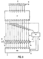
- Figure 9 shows another embodiment of the converter in which detection of the situations where a modified encoding is required is done based on the channel words generated by an unmodified coding as per table I.
- the converter of figure 9 includes a detector 70' having 12 inputs for receiving the four subsequent 3-bit channel words obtained by means of an unmodified encoding as per table I in the circuit LC'.
- the detector 70' detects whether the two subsequent 3-bit channel words at the outputs o 1 to o 6 of the circuit LC', obtained using the unmodified coding, equal one of the four 6-bit sequences given in the middle column under 'unmodified coding' of table II. If so, the detector 70' issues a switching signal at its output 72 and an address signal AD at its output 72'.
- the switching signal is applied to a switching signal input 65 of the shift register 64'.
- the address signal AD is applied to an address signal input 76 of a ROM 77.
- the detector 70' generates one of four possible address signals AD1 to AD4, in response to the detection of a corresponding one of the four 6-bit sequences in the middle column of table II.
- the address signal AD1 is generated when the detector 70' detects the sequence '101101' and generates the address signal AD4 upon detection of the 6-bit sequence '001100'.
- the ROM 77 has the 6-bit sequences shown in the right column of table II stored. Upon the receipt of the address signal AD1, the ROM supplies the 6-bit sequence ' 100 010' at its outputs o 1 to o 6 , and upon the receipt of the address signal AD2, the ROM supplies the 6-bit sequence ' 101 010' at those outputs.
- the ROM Upon the receipt of the address signal AD3, the ROM supplies the 6-bit sequence '000 010' at those outputs, and upon the receipt of the address signal AD4, the ROM supplies the 6-bit sequence '001 010' at those outputs.
- Each memory location of the shift register 64' has now two inputs, one of them being coupled with a corresponding output of the logic circuit LC', the other being coupled to a corresponding output of the ROM 77.
- the shift register In response to the switching signal applied to the input 75, the shift register accepts the information supplied to its lower inputs and shifts its contents over six positions to the left. As a result, a modified 6-bit sequence is supplied by the shift register 64' to the output 68.
- the detector 70' also detects whether the three subsequent 3-bit channel words at the outputs o 1 to o 9 of the circuit LC', obtained using the unmodified coding, equal one of the four 9-bit sequences given in the middle column under 'unmodified coding' of table III. If so, the detector 70' issues a switching signal at its output 72 and an address signal AD at its output 72'.
- the detector 70' generates one of four possible address signals AD5 to AD8, in response to the detection of a corresponding one of the four 9-bit sequences in the middle column of table III.
- the address signal AD5 is generated when the detector 70' detects the sequence '000 000 000' and generates the address signal AD8 upon detection of the 9-bit sequence '100 000 000'.
- the ROM 77 has the 9-bit sequences shown in the right column of table III stored.
- the ROM supplies the 9-bit sequence '000 010 010' at its outputs o 1 to o 9
- the ROM supplies the 9-bit sequence '001 010 010' at those outputs.
- the ROM supplies the 9-bit sequence ' 101 010 010' at those outputs
- the ROM supplies the 9-bit sequence '100 010 010' at those outputs.
- the shift register In response to the switching signal applied to the input 75, the shift register accepts the information supplied to its lower inputs and shifts its contents over nine positions to the left. As a result, a modified 9-bit sequence is supplied by the shift register 64' to the output 68.
- the detector 70' further detects whether the four subsequent 3-bit channel words at the outputs o 1 to o 12 of the circuit LC', obtained using the unmodified coding, equal one of the following two 12-bit sequences: '101 010 101 010' or '001 010 101 010'. If so, the detector 70' issues a switching signal at its output 72 and an address signal AD at its output 72'. The detector 70' generates one of two possible address signals AD9 and AD10, respectively, in response to the detection of a corresponding one of the two 12-bit sequences given above.
- the address signal AD9 is generated when the detector 70' detects the sequence '101 010 101 010' and generates the address signal AD10 upon detection of the 12-bit sequence '001 010 010 101'.
- the ROM 77 has the 12-bit sequences shown in the right column of table IV stored. Upon the receipt of the address signal AD9, the ROM supplies the 12-bit sequence '100 010 010 010' at its outputs o 1 to o 12 , and upon the receipt of the address signal AD10, the ROM supplies the 12-bit sequence '000 010 010 010' at those outputs.
- the shift register In response to the switching signal applied to the input 75, the shift register accepts the information supplied to its lower inputs and shifts its contents over twelve positions to the left. As a result, a modified 12-bit sequence is supplied by the shift register 64' to the output 68.
- the reshuffling unit 90 is adapted to carry out a reshuffling operation on each second group of said groups of x.n bits in the said replica of the shuffled composite binary source signal, more specifically, by repositioning q bits of a second group of x.n bits into another position in the said group of x.n bits. This results in a replica of the composite binary source signal at the output 92.
- the deleting unit 96 deletes the q-bit merging words present in said replica of the composite binary source signal, resulting in a replica of the binary source signal at the output 98, which replica is supplied to the output terminal 100.
- the reshuffling operation comprises the step of repositioning said p bits such that the n-bit words in the replica of the composite binary source signal are aligned with the n-bit words in the replica of the binary source signal.
- Figure 11 shows a slightly modified version of the decoding device of figure 10.
- the decoding device of figure 11 is for converting a channel signal comprising 3-bit channel words into a replica of the binary source signal comprising 2-bit source words.
- the channel signal is obtained from reading the channel signal from a track on a record carrier, which is either in the form of a magnetic record carrier 36 in longitudinal or disk form, or in the form of an optical record carrier, such as an optical disk 36'.
- a read unit 102 is therefore provided which comprises a read head 104, which is a magnetic read head, when recording the signal on a magnetic record carrier or an optical write head, when recording the signal on an optical record carrier.
- the channel signal thus obtained is converted in the reconverter unit 84', which is adapted to convert subsequent blocks of p consecutive m-bit channel words in said channel signal into corresponding subsequent blocks of p consecutive n-bit words in said shuffled composite binary source signal.
- the reshuffling unit 90' is adapted to reshuffle 1-bit in each second group of x. n bits to another position, as per the shuffling shown in either the figures 4d and 4e or the figures 5d and 5e, so as to obtain the replica of the composite binary source signal.
- the deletion unit 96' deletes the 1-bit merging words from the replica of the composite binary source signal so as to obtain the replica of the binary source signal.
- the switches 42 and 44 are both in their position a-c, so that the serial datastream of the replica of the shuffled composite source signal supplied to the input 7 is directly fed to the output 9. In this way, the words rw,and rw 2 and the merging word mw 0 are supplied to the output 9.
- the switch 42 is switched into its position a-b, at a time instant that the bit b 7 in the word rw 3 appears at the input 7. Further, upon the influence of the control signal on the line 48, this bit b 7 is stored in the memory M.
- the switch 44 now switches over to its position a-c, so that the merging word mw 1 and subsequent words rw i+5 , rw i+6 , .... and so on, appearing at the input 7, can be supplied to the output 9.
- the bit b 7 in the word rw 3 is actually inserted in its original position of the serial datastream of the replica of the composite binary source signal. This is done for each second group of 48 subsequent source bits in the replica of the shuffled composite binary source signal.
- words rw i are stored in the shift register 40 and shifted further to the right in figure 6 in the shift register 40.
- Storage of words is carried out by storing the word rw 1 , and subsequent words thereafter. Storing the information is continued until the word rw 1 is stored in the memory locations M 47 and M 46 , the word rw 2 is stored in the memory locations M 45 and M 44 and the merging word mw 0 is stored in the memory location M 43 .
- the switches 42 and 44 now switch over to their positions a-c, so that the bit b 0 is supplied to the output 9.
- the switches 42 and 44 are again positioned into their position a-b, so that the bit b 1* , stored in the memory location M 47' and the subsequent words rw 4 , rw 5 , ... stored in the shift register 40, can be supplied to the output 9.
- the bit b 0 is actually inserted in its original position in the serial datastream of the replica of the composite signal. This is done for each second group of 48 subsequent source bits in the replica of the shuffled composite binary source signal.
- Figure 12 shows an embodiment of the reconverter unit 84' of figure 11 for decoding the channel signal so as to obtain said replica of the shuffled composite binary source signal.
- the converter unit 84' has an input 150 for receiving the channel signal, which input terminal 150 is coupled to an input 156 of a shift register 151, comprising twelve cells Y 1 to Y 12 .
- the shift register 151 functions as a serial-parallel converter so that blocks of four 3-bit channel words are applied to inputs i, to i 12 of a logic circuit 152.
- the logic circuit 152 comprises the four tables I, II, III and IV.
- Outputs o 1 to o 8 of the logic circuit 152 are coupled to inputs of cells X 1 to X 8 of a shift register 154, which has an output 157 coupled to an output terminal 155.
- a detector circuit 153 is present having inputs i, to i 9 , schematically indicated by the reference number 160, coupled to outputs of cells Y 4 to Y 12 respectively of the shift register 151, and outputs o 1 , o 2 and o 3 coupled to control inputs c 1 , c 2 and c 3 , respectively, of the logic circuit 152.
- the detector circuit 153 is capable of
- the detector circuit 153 Upon detection of the '010 010 010' bitpattem, the detector circuit 153 generates a control signal on its output o 1 , upon detection of the '010 010' bit pattern in the cells Y 4 to Y 9 , the detector circuit 153 generates a control signal on its output o 2 , upon detection of the '010' pattern in the cells Y 4 to Y 6 , the detector circuit 153 generates a control signal at its output 0 3 , whilst, when there is no '010' bit pattern in the cells Y 4 to Y 12 , it generates no control signal on its outputs.
- the logic circuit 152 converts the 3-bit channel word stored in the cells Y 1 , Y 2 and Y 3 into its corresponding 2-bit word, as per the conversion table I, and supplies the 2-bit word to the cells X 1 and X 2 .
- the logic circuit 152 converts the block of two 3-bit channel words stored in the cells Y 1 to Y 6 into a block of two 2-bit words, as per the conversion table II, and supplies the two 2-bit words to the cells X 1 to X 4 .
- Figure 13a shows again the serial datastream of the binary source signal.
- Figure 13b shows how a merging word mw 0 is inserted before the source word sw 1 and a merging word mw 1 is inserted before the source word sw i .
- the shuffling step now comprises repositioning the bit b 4 of the byte B 5 , that is: the first bit of the word sw 23 .
- the result of the merging and shuffling step is shown by the signal of figure 13b, which shows the shuffled composite signal in the form of 2-bit words w 1 , w 2 , .... w i , w i+1 , «
- the insertion of the merging word mw 0 in fact means a shift of the source words in the source signal over two bit times, whilst the bit b 4 of the byte B 5 is stored in the second bit position of the word w 1 .
- This is schematically shown by the arrow 154 in figure 13b.
- the following source words sw 1 , sw 2 , .... are shifted over two bit positions.
- the third group of y bits shown in figure 13a again the last bit of the group os shifted to a location in front of the first bit in the group. This is schematically shown by the arrow 154' in figure 13a and 13b.
- An error occurring during the conversion/reconversion step results in an erroneous word rw i in the replica of the shuffled composite signal of figure 13d.
- rw i in the replica of the shuffled composite signal of figure 13d As the boundaries between the words rw i in the signal of figure 13d and the words rsw i in the signal of figure 13e are aligned, such error results in only one 2-bit word, and thus only one byte, to be erroneous, so that no error propagation occurs.
- the converter unit of figure 12 could be modified into a converter unit in which the detector 153 detects the various modified decoding situations from the decoded information, instead of from the encoded information, as disclosed in figure 12.
Landscapes
- Engineering & Computer Science (AREA)
- Theoretical Computer Science (AREA)
- Signal Processing For Digital Recording And Reproducing (AREA)
- Dc Digital Transmission (AREA)
- Television Signal Processing For Recording (AREA)
- Compression, Expansion, Code Conversion, And Decoders (AREA)
- Error Detection And Correction (AREA)
Claims (29)
- Un dispositif pour coder un train de bits de données d'un signal source binaire en un train de bits de données d'un signal de canal binaire, le signal source binaire comprenant une séquence de mots sources à n bits consécutifs et le signal de canal binaire comprenant une séquence de mots de canal à m bits consécutifs, le dispositif comprenant :- des moyens d'entrée (1) pour recevoir le signal source binaire,- des moyens de fusionnement (4) pour recevoir un premier signal d'entrée qui est égal au signal source binaire et pour fusionner chaque fois un mot de fusionnement à q bits entre des groupes successifs de y bits consécutifs dans ledit premier signal d'entrée, en réponse à un signal de commande,- des moyens générateurs de signal de commande (24) pour générer ledit signal de commande,- des moyens de redistribution (8) pour recevoir ledit signal source binaire fusionné avec lesdits mots de fusionnement à q bits dans lesdits moyens de fusionnement (4), et pour effectuer une opération de redistribution sur chaque second groupe desdits groupes de y bits consécutifs, les étapes combinées de fusionnement dans lesdits moyens de fusionnement (4) et de redistribution dans lesdits moyens de redistribution (8) conduisant à un signal source binaire composite redistribué, comprenant une séquence de mots à n bits, y, n et q étant des entiers pour lesquels on a : y > 1, n > 1 et q ≥ 1,- des moyens de conversion (10) pour convertir le signal source binaire composite redistribué en ledit signal de canal binaire, en convertissant des blocs successifs de p mots à n bits consécutifs dans ledit signal source binaire composite redistribué en des blocs successifs correspondants de p mots de canal à m bits consécutifs dans ledit signal de canal binaire, m et p étant des entiers pour lesquels on a m > n, p ≥ 1 et où p peut varier,- des moyens de sortie (20) pour délivrer ledit signal de canal binaire,l'opération de redistribution comprenant l'étape de repositionnement dans chacun desdits seconds groupes de y bits consécutifs, de q bits dans le second groupe de y bits consécutifs à une autre position dans le second groupe de y bits consécutifs, de façon à ce que, à l'exception des mots à n bits comprenant un mot de fusionnement à q bits, les mots à n bits dudit signal source binaire composite redistribué, exigés pour la conversion en des mots de canal à m bits, soient alignés avec les mots sources à n bits dudit signal source binaire, et que n = 2q.
- Dispositif selon la revendication 1, caractérisé en ce que y = x.n, de sorte que chaque groupe de y bits comprend x mots sources à n bits consécutifs, où x est un entier supérieur à 1.
- Dispositif selon la revendication 1, caractérisé en ce que l'opération de redistribution comprend l'étape de repositionnement dans le second groupe de y bits consécutifs des q derniers bits du groupe de y bits consécutifs à une position précédant le premier bit dans ledit groupe de y bits consécutifs.
- Dispositif selon la revendication 2, caractérisé en ce que l'opération de redistribution comprend l'étape de repositionnement dans un second groupe de x mots sources à n bits consécutifs, de q bits du dernier mot source dans le groupe des x mots sources consécutifs à une position précédant le premier mot source à n bits dans ledit groupe de x mots sources consécutifs.
- Dispositif selon la revendication 4, caractérisé en ce que l'opération de redistribution comprend l'étape de repositionnement dans ledit second groupe des x mots sources à n bits consécutifs, des derniers q bits du dernier mot source dans le groupe des x mots sources consécutifs à une position précédant directement le premier mot source à n bits dans ledit groupe des x mots sources consécutifs.
- Dispositif selon la revendication 1, caractérisé en ce que l'opération de redistribution comprend l'étape de repositionnement dans le second groupe de y bits consécutifs, des q premiers bits du groupe à une position faisant suite au dernier bit dudit groupe de y bits consécutifs.
- Dispositif selon la revendication 2, caractérisé en ce que l'opération de redistribution comprend l'étape de repositionnement dans un second groupe des x mots sources à n bits consécutifs, de q bits du premier mot source dans le groupe des x mots sources consécutifs à une position faisant suite au dernier mot source à n bits dans ledit groupe des x mots sources consécutifs.
- Dispositif selon la revendication 7, caractérisé en ce que l'opération de redistribution comprend l'étape de repositionnement dans ledit second groupe des x mots sources à n bits consécutifs, des q premiers bits du premier mot source dans le groupe des x mots sources consécutifs à une position faisant directement suite au dernier mot source à n bits dans ledit groupe des x mots sources consécutifs.
- Dispositif selon l'une quelconque des revendications précédentes, caractérisé en ce que lesdits moyens de conversion (10) sont aptes à convertir un bloc de p mots à n bits consécutifs dans le signal source binaire composite redistribué en un bloc correspondant de p mots de canal à m bits consécutifs, de façon à ce que la conversion pour chaque bloc de p mots à n bits consécutifs du signal source binaire composite redistribué conserve la parité.
- Dispositif selon l'une quelconque des revendications précédentes, caractérisé en ce que m = 3.n/2.
- Dispositif selon la revendication 10, caractérisé en ce que n = 2.
- Dispositif selon la revendication 11, caractérisé en ce que le dispositif est apte à convertir des mots uniques dans le signal source binaire composite redistribué en des mots de canal uniques correspondants selon le tableau suivant :
Mot à 2 bits Mot de canal 00 101 01 100 10 001 11 000 - Dispositif selon la revendication 11 ou 12, dans lequel les moyens de conversion (10) sont aptes à convertir des mots à 2 bits dans le signal source binaire composite redistribué en des mots de canal 3 bits correspondants afin d'obtenir un signal de canal sous la forme d'une séquence (d, k), où d =1, le dispositif comprenant en outre des moyens 70 pour détecter la position dans le train binaire du signal source binaire composite redistribué lorsque le codage de mots à 2 bits uniques en des mots de canal uniques correspondants conduirait à une violation de la contrainte d aux limites entre mots de canal et pour délivrer un signal de commande à ladite détection, caractérisé en ce que, en l'absence du signal de commande, les moyens de conversion (10) sont conçus pour convertir des mots à 2 bits uniques dans le signal source binaire composite redistribué en des mots de canal à 3 bits uniques correspondants de façon à ce que la conversion effectuée pour chaque mot à 2 bits conserve la parité.
- Dispositif selon la revendication 13, dans lequel, en présence du signal de commande apparaissant pendant la conversion de deux mots consécutifs du signal source binaire composite redistribué, les moyens de conversion (10) sont aptes à convertir un bloc desdits deux mots à 2 bits consécutifs en un bloc de deux mots de canal à 3 bits correspondants, de façon à ce que l'un des deux mots du bloc de mots à 2 bits soit converti en un mot de canal à 3 bits qui n'est pas identique à l'un des quatre mots de canal utilisés dans la conversion de mots à 2 bits uniques, afin de conserver la contrainte d = 1,
caractérisé en ce que, en présence dudit signal de commande, les moyens de conversion (10) sont en outre aptes à convertir le bloc desdits deux mots à 2 bits consécutifs en un bloc correspondant de deux mots de canal à 3 bits successifs, de façon à ce que la conversion effectuée pour ledit bloc de deux mots à 2 bits successifs conserve la parité. - Dispositif selon la revendication 14, caractérisé en ce que les moyens de conversion (10) sont aptes à convertir les blocs de deux mots à 2 bits consécutifs en les blocs de deux mots de canal à 3 bits consécutifs selon le codage donné dans le tableau suivant :
Bloc de mots à 2 bits Bloc de 2 mots de canal 00 00 100 010 00 01 101 010 10 00 000 010 10 01 001 010 - Dispositif selon la revendication 14 ou 15, dans lequel k a une valeur supérieure à 5, le dispositif étant en outre muni de moyens (70) pour détecter la position dans le train binaire du signal source binaire composite redistribué à laquelle un codage de mots à 2 bits uniques en des mots de canal à 3 bits uniques conduirait à une violation de la contrainte k et pour délivrer un second signal de commande en réponse à ladite détection, caractérisé en ce que, en présence du second signal de commande apparaissant pendant la conversion de trois mots à 2 bits consécutifs dans le signal source binaire composite redistribué, les moyens de conversion (10) sont aptes à convertir un bloc desdits trois mots à 2 bits consécutifs en un bloc de trois mots de canal à 3 bits correspondants, de façon à ce que la conversion dudit bloc de trois mots à 2 bits conserve la parité, les moyens de conversion (10) étant en outre aptes à convertir deux des trois mots du bloc de trois mots à 2 bits en des mots de canal à 3 bits correspondants non identiques aux quatre mots de canal utilisés pour convertir des mots à 2 bits uniques, afin de conserver la contrainte k.
- Dispositif selon la revendication 16, caractérisé en ce que les moyens de conversion (10) sont aptes à convertir des blocs de trois mots à 2 bits consécutifs en des blocs de 3 mots de canal à 3 bits consécutifs selon le codage donné dans le tableau suivant :
Bloc de mots à 2 bits Bloc de 3 mots canal 11 11 11 000 010 010 11 11 10 001 010 010 01 11 10 101 010 010 01 11 11 100 010 010 - Dispositif pour décoder un train de bits de données d'un signal de canal binaire tel qu'il est généré par un dispositif selon la revendication 1, en un train de bits de données d'un signal source binaire selon la revendication 1, le dispositif comprenant :- des moyens d'entrée (80) pour recevoir le signal de canal binaire,- des moyens de reconversion (84) pour convertir le signal de canal binaire en un signal source binaire composite, les moyens de reconversion (84) étant aptes à convertir le signal de canal binaire en un signal source binaire composite redistribué en convertissant des blocs successifs de p mots de canal à m bits consécutifs dans ledit signal de canal en des blocs successifs correspondants de p mots à n bits consécutifs dans ledit signal source binaire composite redistribué, des mots de fusionnement à q bits étant présents à des positions équidistantes dans le signal source binaire composite redistribué, des mots de fusionnement à q bits successifs dans ledit signal redistribué étant séparés par des groupes de y bits dans ledit signal source binaire composite redistribué,- des moyens de redistribution (90) pour effectuer une opération de redistribution sur chaque second groupe de y bits dudit signal source binaire composite redistribué en repositionnant q bits à une autre position à l'intérieur de chaque second groupe de y bits,- des moyens d'élimination (96) pour éliminer lesdits mots de fusionnement à q bits, les étapes combinées de redistribution dans lesdits moyens de redistribution (90) et d'élimination dans lesdits moyens d'élimination (96) conduisant au signal source binaire comprenant une séquence de mots sources à n bits,- des moyens de sortie (100) pour délivrer ledit signal source binaire,
caractérisé en ce que y est un entier supérieur à 1, n et q sont des entiers pour lesquels on a n = 2q et q ≥ 1, m et p sont des entiers pour lesquels on a m > n > 1, p ≥ 1, et où p peut varier. - Dispositif selon la revendication 18, caractérisé en ce que y=x.n, de sorte que chaque groupe de y bits comprend x mots sources à n bits consécutifs, où x est un entier supérieur à 1.
- Dispositif selon la revendication 18, caractérisé en ce que l'opération de redistribution comprend l'étape de repositionnement dans le second groupe de y bits, des q premiers bits du groupe de y bits à une position faisant suite au dernier bit dans ledit groupe de y bits.
- Dispositif selon la revendication 18, caractérisé en ce que l'opération de redistribution comprend l'étape de repositionnement dans le second groupe de y bits du signal redistribué, des q premiers bits du groupe de y bits à une position précédant les q derniers bits dudit groupe de y bits.
- Dispositif selon la revendication 18, caractérisé en ce que l'opération de redistribution comprend l'étape de repositionnement dans le second groupe de y bits du signal redistribué, des q derniers bits du groupe de y bits étant à une position précédant le premier bit dudit groupe de y bits.
- Dispositif selon la revendication 18, caractérisé en ce que l'opération de redistribution comprend l'étape de repositionnement dans le second groupe de y bits du signal redistribué, des q derniers bits du groupe de y bits à une position faisant suite aux q premiers bits dudit groupe de y bits.
- Dispositif d'enregistrement pour enregistrer un signal de canal sur une piste d'un support d'enregistrement (36'), le dispositif d'enregistrement comprenant le dispositif de codage selon l'une quelconque des revendications 1 à 17 et comprenant des moyens d'écriture (34) pour écrire le signal de canal généré par ledit dispositif de codage sur ladite piste du support d'enregistrement (36').
- Dispositif d'enregistrement selon la revendication 24, caractérisé en ce qu'il comprend en outre des moyens de pré-codage de type 1 T (16') pour pré-coder le signal de canal avant d'écrire le signal de canal sur la piste du support d'enregistrement (36').
- Support d'enregistrement (36'), comprenant un signal de canal sur une piste obtenue avec le dispositif d'enregistrement selon la revendication 24 ou 25.
- Support d'enregistrement (36') selon la revendication 26, dans lequel le support d'enregistrement (36') est un support d'enregistrement optique.
- Dispositif de reproduction pour reproduire un signal de canal à partir d'une piste d'un support d'enregistrement (36'), le dispositif de reproduction comprenant le dispositif de décodage selon l'une quelconque des revendications 18 à 23 et comprenant des moyens de lecture (102) pour lire le signal de canal depuis ladite piste.
- Procédé de codage d'un train de bits de données d'un signal source binaire en un train de bits de données d'un signal de canal binaire, le signal source binaire comprenant une séquence de mots sources à n bits consécutifs et le signal de canal binaire comprenant une séquence de mots de canal à n bits consécutifs, le procédé comprenant les étapes de :- réception du signal source binaire,- réception d'un premier signal d'entrée qui est égal au signal source binaire et fusionnement d'un mot de fusionnement à q bits chaque fois entre des groupes successifs de y bits consécutifs dans ledit premier signal d'entrée dans des moyens de fusionnement (4) en réponse à un signal de commande,- génération dudit signal de commande,- réception dudit signal source binaire fusionné avec lesdits mots de fusionnement à q bits dans lesdits moyens de fusionnement (4), et exécution d'une opération de redistribution sur chaque second groupe desdits groupes de y bits consécutifs,les étapes combinées de fusionnement et de redistribution conduisant à un signal source binaire composite redistribué comprenant une séquence de mots à n bits, y, n et q étant des entiers pour lesquels on a : y>1, n>1, et q≥1,- conversion du signal source binaire composite redistribué en ledit signal de canal binaire en convertissant des blocs successifs de p mots à n bits consécutifs dans ledit signal source binaire composite redistribué en des blocs successifs correspondants de p mots de canal à m bits consécutifs dans ledit signal de canal binaire, m et p étant des entiers pour lesquels on a : m > n, p ≥ 1 et où p peut varier,- délivrer ledit signal de canal binaire, l'opération de redistribution comprenant l'étape de repositionnement dans chacun desdits seconds groupes de y bits consécutifs, de q bits du groupe à une autre position dans ledit groupe, de façon à ce que, à l'exception des mots à n bits comprenant un mot de fusionnement à q bits, les mots à n bits dans ledit signal source binaire composite redistribué, exigés pour la conversion en des mots de canal à m bits, soient alignés avec les mots sources à n bits dudit signal source binaire, et que n = 2q.
Priority Applications (1)
| Application Number | Priority Date | Filing Date | Title |
|---|---|---|---|
| EP99900067A EP0965172B1 (fr) | 1998-01-09 | 1999-01-08 | Dispositif de codage/decodage de mots source de n bits en mots canal correspondants de m bits, et vice versa |
Applications Claiming Priority (6)
| Application Number | Priority Date | Filing Date | Title |
|---|---|---|---|
| EP98200041 | 1998-01-09 | ||
| EP98200041 | 1998-01-09 | ||
| EP98202491 | 1998-07-24 | ||
| EP98202491 | 1998-07-24 | ||
| PCT/IB1999/000011 WO1999035747A2 (fr) | 1998-01-09 | 1999-01-08 | Dispositif de codage/decodage de mots source de n bits en mots de canal correspondants de m bits, et vice versa |
| EP99900067A EP0965172B1 (fr) | 1998-01-09 | 1999-01-08 | Dispositif de codage/decodage de mots source de n bits en mots canal correspondants de m bits, et vice versa |
Publications (2)
| Publication Number | Publication Date |
|---|---|
| EP0965172A2 EP0965172A2 (fr) | 1999-12-22 |
| EP0965172B1 true EP0965172B1 (fr) | 2006-03-01 |
Family
ID=26149968
Family Applications (1)
| Application Number | Title | Priority Date | Filing Date |
|---|---|---|---|
| EP99900067A Expired - Lifetime EP0965172B1 (fr) | 1998-01-09 | 1999-01-08 | Dispositif de codage/decodage de mots source de n bits en mots canal correspondants de m bits, et vice versa |
Country Status (8)
| Country | Link |
|---|---|
| US (1) | US6265994B1 (fr) |
| EP (1) | EP0965172B1 (fr) |
| JP (1) | JP4138031B2 (fr) |
| KR (1) | KR100701258B1 (fr) |
| CN (2) | CN1190901C (fr) |
| AT (1) | ATE319226T1 (fr) |
| DE (1) | DE69930101T2 (fr) |
| WO (1) | WO1999035747A2 (fr) |
Families Citing this family (14)
| Publication number | Priority date | Publication date | Assignee | Title |
|---|---|---|---|---|
| CN1298573A (zh) * | 1998-12-21 | 2001-06-06 | 皇家菲利浦电子有限公司 | 用于把n-位源字编码为相应的m-位信道字以及把m-位信道字解码为相应的n-位源字的设备 |
| BR9908073A (pt) * | 1998-12-21 | 2000-10-24 | Koninkl Philips Electronics Nv | Dispositivo e processo para codificar uma corrente de bits de dados de um sinal fonte binário, sinal de canal binário, portadora de gravação, e, dispositivo decodificador de uma corrente de bits de dados de um sinal de canal binário |
| WO2001095495A1 (fr) * | 2000-06-02 | 2001-12-13 | Koninklijke Philips Electronics N.V. | Dispositif pour coder une sequence binaire de donnees d'un signal source ginaire en une sequence binaire de donnees d'un signal canal binaire, memoire, enregistreur d'information, support d'enregistrement, codeur et appareil de reproduction |
| US6661355B2 (en) * | 2000-12-27 | 2003-12-09 | Apple Computer, Inc. | Methods and apparatus for constant-weight encoding & decoding |
| KR100669623B1 (ko) * | 2001-03-12 | 2007-01-15 | 엘지전자 주식회사 | 디지털 데이터 변환방법 |
| DE10134472B4 (de) * | 2001-07-16 | 2005-12-15 | Infineon Technologies Ag | Sende- und Empfangsschnittstelle und Verfahren zur Datenübertragung |
| US6476737B1 (en) * | 2001-11-16 | 2002-11-05 | Lsi Logic Corporation | Rate 64/65 (d=0, G=11/I=10) run length limited modulation code |
| US6917313B1 (en) | 2002-01-16 | 2005-07-12 | Marvell International Ltd. | DC-free codes |
| EP1792404A1 (fr) * | 2004-09-15 | 2007-06-06 | Koninklijke Philips Electronics N.V. | Codeur et procede de codage pour codes ayant une contrainte de passage de transition maximale a repetition de r=2 |
| US7307554B2 (en) * | 2004-12-20 | 2007-12-11 | Kawasaki Microelectronics, Inc. | Parallel data transmission method and parallel data transmission system |
| CN101292221B (zh) * | 2005-11-22 | 2012-05-30 | 英特尔公司 | 用于串行链路的基于信号跃迁特征的编码的方法和装置 |
| WO2007110814A1 (fr) * | 2006-03-27 | 2007-10-04 | Koninklijke Philips Electronics N.V. | Appareils et procédés de codage et de décodage |
| KR101355633B1 (ko) * | 2007-11-06 | 2014-01-29 | 삼성전자주식회사 | 인코더 및 인코딩 방법 |
| EP3465974A1 (fr) * | 2016-06-06 | 2019-04-10 | Agilepq, Inc. | Systèmes et procédés de conversion de données |
Family Cites Families (11)
| Publication number | Priority date | Publication date | Assignee | Title |
|---|---|---|---|---|
| US4501000A (en) * | 1981-07-27 | 1985-02-19 | Sony Corporation | Method of coding binary data |
| JPS59131936A (ja) * | 1983-01-19 | 1984-07-28 | Fuji Photo Film Co Ltd | ハロゲン化銀カラ−写真感光材料 |
| NL8402445A (nl) * | 1984-01-20 | 1985-08-16 | Philips Nv | Werkwijze voor het coderen van n-bits informatiewoorden naar m-bits codewoorden, inrichting voor het uitvoeren van die werkwijze, werkwijze voor het decoderen van m-bits codewoorden naar n-bits informatiewoorden en inrichting voor het uitvoeren van die werkwijze. |
| US5477222A (en) * | 1993-05-04 | 1995-12-19 | U.S. Philips Corporation | Device for encoding/decoding N-bit source words into corresponding M-bit channel words, and vice versa |
| EP0655850A3 (fr) * | 1993-10-28 | 1995-07-19 | Philips Electronics Nv | Transmission et réception d'un signal d'information numérique. |
| WO1996019044A1 (fr) * | 1994-12-12 | 1996-06-20 | Sony Corporation | Procede de codage de donnees et procede de decodage de donnees |
| US5604497A (en) * | 1995-10-10 | 1997-02-18 | Lucent Technologies Inc. | Apparatus and method for increasing density of run length limited block codes without increasing error propagation |
| US6061005A (en) * | 1996-11-25 | 2000-05-09 | Microcorp Technologies (Proprietary) Limited | Encoding of data |
| US5847665A (en) * | 1996-12-04 | 1998-12-08 | Holtek Microelectronics Inc. | Method and device of encoding-decoding for actuating system |
| JPH10271016A (ja) * | 1997-03-21 | 1998-10-09 | Kawasaki Steel Corp | 符号/復号化器 |
| HUP0003771A3 (en) * | 1997-12-22 | 2002-11-28 | Koninkl Philips Electronics Nv | Device for encoding/decoding n-bit source words into corresponding m-bit channel words, and vice versa |
-
1999
- 1999-01-08 CN CNB998002348A patent/CN1190901C/zh not_active Expired - Fee Related
- 1999-01-08 US US09/403,681 patent/US6265994B1/en not_active Expired - Fee Related
- 1999-01-08 EP EP99900067A patent/EP0965172B1/fr not_active Expired - Lifetime
- 1999-01-08 CN CNA2004100576915A patent/CN1595811A/zh active Pending
- 1999-01-08 AT AT99900067T patent/ATE319226T1/de active
- 1999-01-08 WO PCT/IB1999/000011 patent/WO1999035747A2/fr not_active Ceased
- 1999-01-08 DE DE69930101T patent/DE69930101T2/de not_active Expired - Lifetime
- 1999-01-08 KR KR1019997008163A patent/KR100701258B1/ko not_active Expired - Fee Related
- 1999-01-08 JP JP53589499A patent/JP4138031B2/ja not_active Expired - Fee Related
Also Published As
| Publication number | Publication date |
|---|---|
| CN1190901C (zh) | 2005-02-23 |
| CN1595811A (zh) | 2005-03-16 |
| DE69930101T2 (de) | 2006-09-14 |
| KR100701258B1 (ko) | 2007-03-29 |
| JP2001515687A (ja) | 2001-09-18 |
| ATE319226T1 (de) | 2006-03-15 |
| DE69930101D1 (de) | 2006-04-27 |
| WO1999035747A3 (fr) | 1999-09-23 |
| CN1375129A (zh) | 2002-10-16 |
| KR20000076075A (ko) | 2000-12-26 |
| EP0965172A2 (fr) | 1999-12-22 |
| JP4138031B2 (ja) | 2008-08-20 |
| WO1999035747A2 (fr) | 1999-07-15 |
| US6265994B1 (en) | 2001-07-24 |
Similar Documents
| Publication | Publication Date | Title |
|---|---|---|
| US6664905B1 (en) | Device for encoding n-bit source words into corresponding m-bit channel words and decoding m-bit channel words into corresponding n-bit source words | |
| US6175318B1 (en) | Device for encoding/decoding n-bit source words into corresponding m-bit channel words, and vice versa | |
| US6265994B1 (en) | Device for encoding/decoding n-bit source words into corresponding m-bit channel words, and vice versa | |
| JP3935217B2 (ja) | mビット情報ワードのシーケンスから変調信号への変換 | |
| WO2001082540A1 (fr) | Dispositif de codage/decodage de mots de source a n-bits en mots de canal a m-bits, et vice-versa | |
| US6225921B1 (en) | Device for encoding/decoding n-bit source words into corresponding m-bit channel words, and vice versa | |
| EP1076932B1 (fr) | CODAGE/DECODAGE DE MOTS SOURCE A n-BITS EN MOTS BINAIRES A m-BITS, ET VICE VERSA, DE MANIERE A OBTENIR UNE CONVERSION A INVERSION DE PARITE | |
| US6545615B2 (en) | Device for encoding a stream of databits of a binary source signal into a stream of databits of a binary channel signal, memory means, device for recording information, record carrier, device for coding and device for playing back | |
| EP0624000B1 (fr) | Dispositif de codage/décodage de mots-sources de n-bits en mots de canal correspondants de m-bits, et vice-versa | |
| JP3848163B2 (ja) | 情報をコーディングする装置及びその方法、そのコーディングされせた情報をデコーディングする装置及びその方法、記録媒体への変調信号の記録方法、記録媒体並びに変調信号の変換方法 | |
| KR100575638B1 (ko) | 정보 코딩을 위한 장치 및 방법과, 그 코딩된 정보를디코딩하기 위한 장치 및 방법과, 변조 신호 및 기록 매체제조방법 | |
| KR100575658B1 (ko) | 정보 코딩을 위한 장치 및 방법 | |
| KR100752880B1 (ko) | 정보를 코딩/디코딩하는 방법 및 장치 | |
| MXPA99007750A (en) | DEVICE FOR ENCODING/DECODING n-BIT SOURCE WORDS INTO CORRESPONDING m-BIT CHANNEL WORDS, AND VICE VERSA | |
| HK1035450B (en) | Encoding/decoding n-bit source words into corresponding m-bit channel words, and vice versa, such that the conversion is parity inverting | |
| MXPA00008156A (es) | Dispositivo para codificar palabras fuente de n bits en palabras de canal de m bits correspondientes y decodificar palabras de canal de m bits en palabras fuentes de bits correspondientes | |
| MXPA99006015A (en) | Device for encoding/decoding n-bit source words into corresponding m-bit channel words, and vice versa |
Legal Events
| Date | Code | Title | Description |
|---|---|---|---|
| PUAI | Public reference made under article 153(3) epc to a published international application that has entered the european phase |
Free format text: ORIGINAL CODE: 0009012 |
|
| 17P | Request for examination filed |
Effective date: 19991011 |
|
| AK | Designated contracting states |
Kind code of ref document: A2 Designated state(s): AT BE DE FR GB |
|
| 17Q | First examination report despatched |
Effective date: 20040406 |
|
| GRAP | Despatch of communication of intention to grant a patent |
Free format text: ORIGINAL CODE: EPIDOSNIGR1 |
|
| GRAS | Grant fee paid |
Free format text: ORIGINAL CODE: EPIDOSNIGR3 |
|
| GRAA | (expected) grant |
Free format text: ORIGINAL CODE: 0009210 |
|
| AK | Designated contracting states |
Kind code of ref document: B1 Designated state(s): AT BE DE FR GB |
|
| REG | Reference to a national code |
Ref country code: GB Ref legal event code: FG4D |
|
| REF | Corresponds to: |
Ref document number: 69930101 Country of ref document: DE Date of ref document: 20060427 Kind code of ref document: P |
|
| ET | Fr: translation filed | ||
| PLBE | No opposition filed within time limit |
Free format text: ORIGINAL CODE: 0009261 |
|
| STAA | Information on the status of an ep patent application or granted ep patent |
Free format text: STATUS: NO OPPOSITION FILED WITHIN TIME LIMIT |
|
| 26N | No opposition filed |
Effective date: 20061204 |
|
| PGFP | Annual fee paid to national office [announced via postgrant information from national office to epo] |
Ref country code: FR Payment date: 20110217 Year of fee payment: 13 Ref country code: AT Payment date: 20110127 Year of fee payment: 13 |
|
| PGFP | Annual fee paid to national office [announced via postgrant information from national office to epo] |
Ref country code: DE Payment date: 20110328 Year of fee payment: 13 Ref country code: BE Payment date: 20110224 Year of fee payment: 13 Ref country code: GB Payment date: 20110131 Year of fee payment: 13 |
|
| BERE | Be: lapsed |
Owner name: KONINKLIJKE *PHILIPS ELECTRONICS N.V. Effective date: 20120131 |
|
| GBPC | Gb: european patent ceased through non-payment of renewal fee |
Effective date: 20120108 |
|
| REG | Reference to a national code |
Ref country code: FR Ref legal event code: ST Effective date: 20120928 |
|
| PG25 | Lapsed in a contracting state [announced via postgrant information from national office to epo] |
Ref country code: DE Free format text: LAPSE BECAUSE OF NON-PAYMENT OF DUE FEES Effective date: 20120801 Ref country code: GB Free format text: LAPSE BECAUSE OF NON-PAYMENT OF DUE FEES Effective date: 20120108 |
|
| REG | Reference to a national code |
Ref country code: DE Ref legal event code: R119 Ref document number: 69930101 Country of ref document: DE Effective date: 20120801 |
|
| REG | Reference to a national code |
Ref country code: AT Ref legal event code: MM01 Ref document number: 319226 Country of ref document: AT Kind code of ref document: T Effective date: 20120108 |
|
| PG25 | Lapsed in a contracting state [announced via postgrant information from national office to epo] |
Ref country code: BE Free format text: LAPSE BECAUSE OF NON-PAYMENT OF DUE FEES Effective date: 20120131 Ref country code: FR Free format text: LAPSE BECAUSE OF NON-PAYMENT OF DUE FEES Effective date: 20120131 |
|
| PG25 | Lapsed in a contracting state [announced via postgrant information from national office to epo] |
Ref country code: AT Free format text: LAPSE BECAUSE OF NON-PAYMENT OF DUE FEES Effective date: 20120108 |