EP0965862A2 - Planar microlens array and method of manufacturing same - Google Patents
Planar microlens array and method of manufacturing same Download PDFInfo
- Publication number
- EP0965862A2 EP0965862A2 EP99304747A EP99304747A EP0965862A2 EP 0965862 A2 EP0965862 A2 EP 0965862A2 EP 99304747 A EP99304747 A EP 99304747A EP 99304747 A EP99304747 A EP 99304747A EP 0965862 A2 EP0965862 A2 EP 0965862A2
- Authority
- EP
- European Patent Office
- Prior art keywords
- refractive index
- thickness
- synthetic resin
- microlenses
- glass plate
- Prior art date
- Legal status (The legal status is an assumption and is not a legal conclusion. Google has not performed a legal analysis and makes no representation as to the accuracy of the status listed.)
- Granted
Links
- 238000004519 manufacturing process Methods 0.000 title description 4
- 229920003002 synthetic resin Polymers 0.000 claims abstract description 43
- 239000000057 synthetic resin Substances 0.000 claims abstract description 43
- 239000012790 adhesive layer Substances 0.000 claims abstract description 26
- 239000006059 cover glass Substances 0.000 claims abstract description 20
- 239000006121 base glass Substances 0.000 claims abstract description 12
- 238000000034 method Methods 0.000 claims description 6
- 238000003491 array Methods 0.000 claims 1
- 230000015572 biosynthetic process Effects 0.000 claims 1
- 239000004973 liquid crystal related substance Substances 0.000 description 14
- 239000011521 glass Substances 0.000 description 7
- 239000000463 material Substances 0.000 description 7
- 239000000758 substrate Substances 0.000 description 7
- 239000010410 layer Substances 0.000 description 4
- 239000003822 epoxy resin Substances 0.000 description 2
- 125000001153 fluoro group Chemical group F* 0.000 description 2
- 229920000647 polyepoxide Polymers 0.000 description 2
- 238000007493 shaping process Methods 0.000 description 2
- 239000011800 void material Substances 0.000 description 2
- 239000004925 Acrylic resin Substances 0.000 description 1
- 229920000178 Acrylic resin Polymers 0.000 description 1
- 239000003795 chemical substances by application Substances 0.000 description 1
- 238000010438 heat treatment Methods 0.000 description 1
- 239000012528 membrane Substances 0.000 description 1
- 230000003287 optical effect Effects 0.000 description 1
- 230000005855 radiation Effects 0.000 description 1
- 239000010409 thin film Substances 0.000 description 1
Images


Classifications
-
- G—PHYSICS
- G02—OPTICS
- G02B—OPTICAL ELEMENTS, SYSTEMS OR APPARATUS
- G02B3/00—Simple or compound lenses
- G02B3/0006—Arrays
- G02B3/0012—Arrays characterised by the manufacturing method
- G02B3/0031—Replication or moulding, e.g. hot embossing, UV-casting, injection moulding
-
- G—PHYSICS
- G02—OPTICS
- G02B—OPTICAL ELEMENTS, SYSTEMS OR APPARATUS
- G02B3/00—Simple or compound lenses
- G02B3/0006—Arrays
- G02B3/0012—Arrays characterised by the manufacturing method
- G02B3/0025—Machining, e.g. grinding, polishing, diamond turning, manufacturing of mould parts
-
- G—PHYSICS
- G02—OPTICS
- G02F—OPTICAL DEVICES OR ARRANGEMENTS FOR THE CONTROL OF LIGHT BY MODIFICATION OF THE OPTICAL PROPERTIES OF THE MEDIA OF THE ELEMENTS INVOLVED THEREIN; NON-LINEAR OPTICS; FREQUENCY-CHANGING OF LIGHT; OPTICAL LOGIC ELEMENTS; OPTICAL ANALOGUE/DIGITAL CONVERTERS
- G02F1/00—Devices or arrangements for the control of the intensity, colour, phase, polarisation or direction of light arriving from an independent light source, e.g. switching, gating or modulating; Non-linear optics
- G02F1/01—Devices or arrangements for the control of the intensity, colour, phase, polarisation or direction of light arriving from an independent light source, e.g. switching, gating or modulating; Non-linear optics for the control of the intensity, phase, polarisation or colour
- G02F1/13—Devices or arrangements for the control of the intensity, colour, phase, polarisation or direction of light arriving from an independent light source, e.g. switching, gating or modulating; Non-linear optics for the control of the intensity, phase, polarisation or colour based on liquid crystals, e.g. single liquid crystal display cells
- G02F1/133—Constructional arrangements; Operation of liquid crystal cells; Circuit arrangements
- G02F1/1333—Constructional arrangements; Manufacturing methods
- G02F1/1335—Structural association of cells with optical devices, e.g. polarisers or reflectors
- G02F1/133526—Lenses, e.g. microlenses or Fresnel lenses
Definitions
- the present invention relates to a planar microlens array used in a liquid crystal display element and so on.
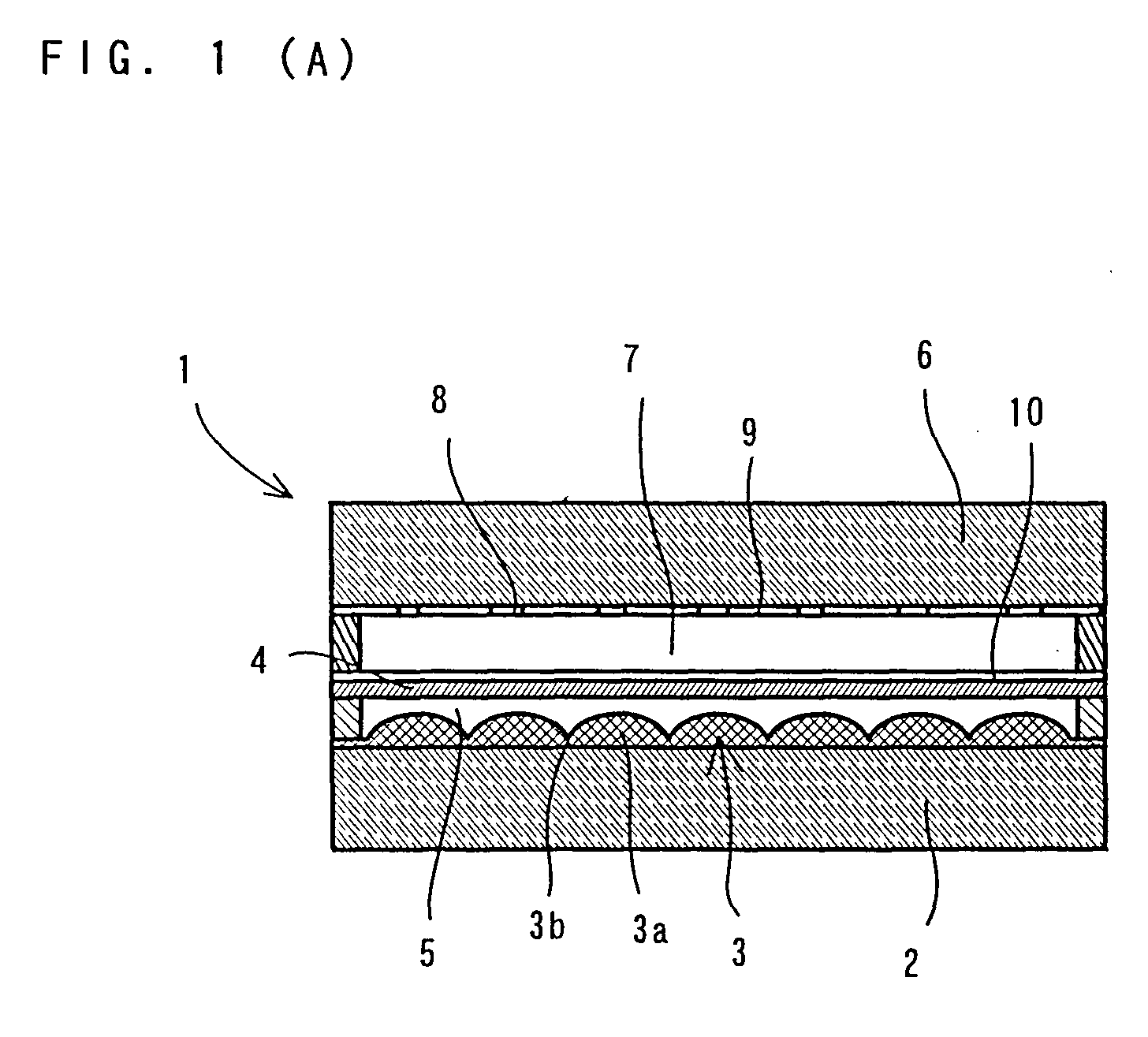
- FIG. 1(A) and FIG. 1(B) of the accompanying drawings Prior-art liquid crystal display elements in which a planar microlens array and a liquid crystal layer are combined are shown in FIG. 1(A) and FIG. 1(B) of the accompanying drawings.
- the liquid crystal display element shown in FIG. 1(A) includes a planar microlens array 1 comprising an array of convex microlenses 3 provided on a surface of a base glass plate 2.
- the array of convex microlenses 3 is covered with a cover glass plate 4 which is bonded to the array of convex microlenses 3 by an adhesive layer 5.
- a liquid crystal layer 7 is filled between the cover glass plate 4 and a TFT (Thin Film Transistor) glass substrate 6.
- the TFT glass substrate 6 supports transparent pixel electrodes 8 on its surface facing the liquid crystal layer 7.
- the surface of the TFT glass substrate 6 includes areas 9 that are free of the transparent pixel electrodes 8 and carry interconnections and TFTs which do not pass applied light. Electrodes 10 which confront the transparent pixel electrodes 8 are mounted on a surface of the cover glass plate 4 that faces the liquid crystal layer 7.
- an array of convex microlenses 3 is provided on a surface of a cover glass plate 4.
- a planar microlens array according to the present invention can be applied to both the liquid crystal display elements shown in FIG. 1(A) and FIG. 1(B).
- the planar microlens array 1 operates as follows: Applied light is converged by the convex microlenses 3 onto the transparent pixel electrodes 8 to brighten an image projected onto a screen.
- a process of manufacturing the planar microlens array 1, the structure of which is mentioned above, is as follows: As shown in FIG. 2(A), a release agent is coated on a shaping surface of a stamper 11 on which convex portions are densely arranged, and a light-curable or heat-curable synthetic resin material having a high refractive index is set on the shaping surface of the stamper 11. Next, as shown in FIG. 2(B), the base glass plate 2 is pushed onto the synthetic resin material, thereby spreading the synthetic resin material, and the synthetic resin material is cured by applying ultraviolet radiation or heating and is shaped to form the convex microlenses 3. Thereafter the stamper 11 is peeled off.
- a light-curable or heat-curable synthetic resin material having a low refractive index is coated onto the convex microlenses 3, and a glass substrate which is made into a cover glass plate 4 is pushed onto the synthetic resin material, thereby spreading the same. Thereafter, the synthetic resin material is cured and finally the planar microlens array 1 is formed by grinding the glass substrate to the thickness of the cover glass plate 4.
- the convex microlenses may be formed on the glass substrate.
- liquid crystal display panels have pixel dimensions ranging from about 40 ⁇ m to 60 ⁇ m. It is expected that the pixel dimensions will be reduced to about 20 ⁇ m to 30 ⁇ m in the future to meet demands for clearer displayed images.
- the convex microlenses 3 Smaller pixel dimensions require the convex microlenses 3 to be reduced in size, resulting in a shorter focal length. For efficient utilization of the applied light, it is necessary that the focal point of the convex microlenses 3 be positioned substantially on the transparent pixel electrodes. To meet such a requirement, the cover glass plate 4 must be reduced in thickness.
- Each of the convex microlenses 3 and the adhesive layer 5 is made of a heat-curable or ultraviolet-curable synthetic resin.
- the synthetic resin shrinks when cured.
- the synthetic resin having a high refractive index which makes the convex microlenses 3 has high Young's modulus and high residual stress.
- the cover glass plate 4 can withstand the shrinkage of the synthetic resin, provided that the cover glass plate 4 has a substantial thickness. However, if the cover glass plate 4 is thinner, it tends to yield and allow the entire planar microlens array 1 to warp upon shrinkage of the synthetic resin, as shown in FIG. 3 of the accompanying drawings. In particular, shrinkage of the synthetic resin having a high refractive index may result in high residual stress. As a result of this, the width of a cell gap which is formed between the planar microlens array 1 and the TFT glass substrate 6 and to which liquid crystal is applied varies between the center and the periphery. Presently the maximum permissible error range of a cell gap in size is 1.5 ⁇ m.
- the Young's modulus of the synthetic resin having a low refractive index which makes the adhesive layer 5 is smaller than that of the synthetic resin having a high refractive index which makes the convex microlenses 3. That does not mainly cause the warpage but does mainly cause the small voids.
- small voids are produced between the convex microlenses 3 and the adhesive layer 5 because the volume shrinkage percentage of the synthetic resin having a low refractive index generally reaches to 6-9%, and further the synthetic resin having a low refractive index has small values in membrane intensity and interface adhesion intensity.
- the inventors of the present invention tested the cause, the incident amount or the like with regard to warpage and small voids.
- FIG. 5(A) and 5(B) show the relation between thickness and warpage of convex microlenses 3 which comprise a synthetic resin having a high refractive index.
- the thickness of convex microlenses 3 is small.
- a thickness thereof is large.
- a thickness of an adhesive layer 5 which comprises a synthetic resin having a low refractive index is equal in both cases.
- a rest portion 3b needs to be formed in the convex microlenses 3 to prevent damage to the stamper.
- the amount of warpage is determined by the sum of the thickness t 1 of the sphere portion 3a and the thickness t 2 of the rest portion 3b (t 1 + t 2 ).
- FIG. 6(A) and 6(B) show the relation between a thickness of an adhesive layer 5 comprised of a synthetic resin having a low refractive index, and small voids.
- a thickness of the adhesive layer 5 is thin.
- the thickness thereof is thick.
- the thickness of convex microlenses 3 comprised of a synthetic resin having a high refractive index is equal in both cases.
- Pixel dimensions of liquid crystal display panels are determined within 14-60 ⁇ m.
- a epoxy resin having a refractive index (n 1 ) of 1.59-1.68 is used as a synthetic resin having a high refractive index.
- a fluoro epoxy resin or a fluoro acrylic resin having a refractive index (n 2 ) of 1.38-1.42 is used as a synthetic resin having a low refractive index.
- a focal length of a lens is automatically determined.
- a focal length of a lens and a kind of a synthetic resin having a high refractive index are determined, a thickness (t 1 ) of a sphere portion of a convex lens is automatically determined.
- a thickness (t 1 ) of a sphere portion varies according to differences in pixel dimensions, a kind of a synthetic resin and so on. However, generally it is within the scope of 5 ⁇ t 1 ⁇ 30 ( ⁇ m).
- the thickness (t 1 ) of a sphere portion of a convex lens is determined by another element. Therefore, the thickness (t 2 ) of a rest portion and the thickness t 3 of the thinnest portion of an adhesive layer have room for adjustment.
- each thickness t 1 , t 2 and t 3 mentioned above is made to vary, and room for adjustment in the thickness t 2 and t 3 are watched, and the most suitable conditions are estimated thereby.
- a planar microlens array which includes an array of microlenses made of a synthetic resin having a high refractive index and formed on a surface of one of a base glass plate and a cover glass plate, and a adhesive layer made of a synthetic resin having a low refractive index standing between the array of microlenses and the other of the base glass plate and the cover glass plate, wherein the equations (Eqs.
- n 1 represents the refractive index of said synthetic resin having a high refractive index
- n 2 represents the refractive index of said synthetic resin having a low refractive index
- t 1 represents the thickness of the thickest portion of the sphere portion of said microlenses
- t 2 represents the thickness of the rest portion of said microlenses
- t 3 represents said thickness of the thinnest portion of said adhesive layer.
- the base glass plate has a thickness of 0.95 mm
- the cover glass plate has a thickness of 0.15 mm
- the base glass plate and the cover glass plate have dimensions of 27 ⁇ 20 mm
- the lenses are arranged squarely and densely
- a pitch of the lenses is 32 ⁇ m
- a refractive index (n 1 ) of the synthetic resin having a high refractive index which makes up the lenses is 1.59
- a refractive index (n 2 ) of the synthetic resin having a low refractive index which makes up the adhesive layer is 1.38
- a thickness (t 1 ) of a sphere portion of the lenses is 10 ⁇ m
- a thickness (t 3 ) of the thinnest portion of the adhesive layer is 10 ⁇ m
- a thickness (t 2 ) of a rest portion of the microlenses is made to vary.
- t 2 The relation between t 2 and an amount of warpage ( ⁇ m) is shown in TABLE 1.
- a thickness (t 2 ) of a rest portion of the microlenses is fixed at 3 ⁇ m and the other conditions are the same as EMBODIMENT 1.
- a thickness (t 1 ) of a sphere portion of the microlenses and a thickness (t 3 ) of the thinnest portion of the adhesive layer are made to vary.
- a thickness (t 1 ) of the thickest portion of a sphere portion of the microlenses, a thickness (t 2 ) of a rest portion of the microlenses and a thickness (t 3 ) of the thinnest portion of the adhesive layer satisfy the equations, 5 ⁇ t 1 ⁇ 30 ( ⁇ m), t 2 ⁇ 6 ( ⁇ m) and t 3 ⁇ 0.2t 1 ( ⁇ m).
Landscapes
- Physics & Mathematics (AREA)
- Engineering & Computer Science (AREA)
- Manufacturing & Machinery (AREA)
- General Physics & Mathematics (AREA)
- Optics & Photonics (AREA)
- Liquid Crystal (AREA)
Abstract
Description
| t2 (µm) | Amount of warpage (µm) |
| 2 | 0.62 |
| 3 | 0.89 |
| 4 | 1.20 |
| 5 | 1.43 |
| 6 | 1.50 |
| 7 | 1.78 |
| 8 | 2.15 |
| 9 | 2.37 |
| 10 | 2.62 |
| 11 | 2.81 |
| 12 | 3.08 |
| t3 (t1=10) | Small voids | t3 (t1=15) | Small voids | t3 (t1=20) | Small voids |
| 1 | × | 1 | × | 1 | × |
| 2 | ○ | 2 | ○ | 2 | ○ |
| 3 | O | 3 | O | 3 | ○ |
| 4 | ○ | 4 | ○ | 4 | ○ |
| 5 | ○ | 5 | ○ | 5 | ○ |
| 6 | o ○ | 6 | ○ | 6 | ○ |
| 7 | o ○ | 7 | o ○ | 7 | ○ |
| 8 | o ○ | 8 | o ○ | 8 | o ○ |
| 9 | o ○ | 9 | o ○ | 9 | o ○ |
| 10 | o ○ | 10 | o ○ | 10 | o ○ |
| 11 | o ○ | 11 | o ○ | 11 | o ○ |
| ×···Small voids were produced all over. | |||||
| O···Small voids were produced only in the periphery of the lens. | |||||
| o ○···No small void was produced. |
Claims (6)
- A planar microlens arrays comprised of an array of microlenses (3) made of a synthetic resin having a high refractive index and formed on a surface of one of a base glass plate (2) or a cover glass plate (4), wherein an adhesive layer (5) made of a synthetic resin having a low refractive index is provided between the array of microlenses and the other of the base glass plate and the cover glass plate,
wherein the equations (Eqs. 1-5) are satisfied, wherein n1 represents the refractive index of said synthetic resin having a high refractive index, n2 represents the refractive index of said synthetic resin having a low refractive index, t1 represents a thickness of a thickest portion of a sphere portion of said microlenses, t2 represents a thickness of a rest portion of said microlenses and t3 represents a thickness of a thinnest portion of said adhesive layer - A planar microlens array according to claim 1 wherein the equation 6 is also satisfied
- A method of producing a planar microlens array having an array of microlenses (3) made of a synthetic resin having a relatively high refractive index and formed on a surface of one of a base glass plate (2) or a cover glass plate (4), wherein an adhesive layer (5) made of a synthetic resin having a relatively low refractive index is provided between the array of microlenses and the other of the base glass plate and the cover glass plate,
and wherein the thickness (t1) of the thickest part of a sphere portion of the microlenses, the thickness (t2) of a rest portion of the microlenses and the thickness (t3) of the thinnest portion of the adhesive layer are set relative to one another so as to minimise any warpage of the planar microlens array and to minimise the formation of voids between the adhesive layer and the sphere portions of the microlens array. - A method of producing a planar microlens array according to claim 3, wherein the thicknesses t1, t2 and t3 are set relative to one another so as to satisfy the equations:
- A method of producing a planar microlens array according to claim 3 or 4, wherein the synthetic resin of the array (3) of microlenses has a refractive index n1, and the synthetic resin of the adhesive layer (5) has a refractive index n2, and wherein the following equations are satisfied:
- A planar microlens array produced by the method of any of claims 3 to 5.
Applications Claiming Priority (2)
| Application Number | Priority Date | Filing Date | Title |
|---|---|---|---|
| JP16982198 | 1998-06-17 | ||
| JP16982198A JP3824425B2 (en) | 1998-06-17 | 1998-06-17 | Flat micro lens array |
Publications (3)
| Publication Number | Publication Date |
|---|---|
| EP0965862A2 true EP0965862A2 (en) | 1999-12-22 |
| EP0965862A3 EP0965862A3 (en) | 2001-12-12 |
| EP0965862B1 EP0965862B1 (en) | 2003-12-10 |
Family
ID=15893534
Family Applications (1)
| Application Number | Title | Priority Date | Filing Date |
|---|---|---|---|
| EP99304747A Expired - Lifetime EP0965862B1 (en) | 1998-06-17 | 1999-06-17 | Planar microlens array and method of manufacturing same |
Country Status (5)
| Country | Link |
|---|---|
| US (1) | US6069740A (en) |
| EP (1) | EP0965862B1 (en) |
| JP (1) | JP3824425B2 (en) |
| DE (1) | DE69913433T2 (en) |
| TW (1) | TW523496B (en) |
Cited By (2)
| Publication number | Priority date | Publication date | Assignee | Title |
|---|---|---|---|---|
| FR2803395A1 (en) * | 1999-12-30 | 2001-07-06 | Commissariat Energie Atomique | FLAT-SIDE SOLID OPTICAL MICROSYSTEM AND METHOD FOR PRODUCING SUCH MICROSYSTEM |
| WO2021180762A1 (en) * | 2020-03-13 | 2021-09-16 | 3D Global Holding Gmbh | Lenticular lens assembly for mounting on a display surface and mounting method |
Families Citing this family (31)
| Publication number | Priority date | Publication date | Assignee | Title |
|---|---|---|---|---|
| JP3938253B2 (en) | 1997-12-26 | 2007-06-27 | 日本板硝子株式会社 | Resin erecting equal-magnification lens array and manufacturing method thereof |
| JPH11211902A (en) * | 1998-01-21 | 1999-08-06 | Micro Opt:Kk | Flat microlens array |
| US6404555B1 (en) * | 1998-07-09 | 2002-06-11 | Seiko Epson Corporation | Micro lens array, method of fabricating the same and display |
| JP2000029011A (en) * | 1998-07-14 | 2000-01-28 | Seiko Epson Corp | Electro-optical device, manufacturing method thereof, and projection display device |
| US6597510B2 (en) | 2001-11-02 | 2003-07-22 | Corning Incorporated | Methods and apparatus for making optical devices including microlens arrays |
| JP2003279748A (en) * | 2002-01-18 | 2003-10-02 | Nitto Denko Corp | Polarizing film and image display device |
| JP3888223B2 (en) * | 2002-05-13 | 2007-02-28 | ソニー株式会社 | Manufacturing method of liquid crystal display element |
| JP4231702B2 (en) * | 2003-01-17 | 2009-03-04 | 日東電工株式会社 | Micro lens array |
| JP4317375B2 (en) * | 2003-03-20 | 2009-08-19 | 株式会社日立製作所 | Nanoprint apparatus and fine structure transfer method |
| JP4269745B2 (en) * | 2003-03-31 | 2009-05-27 | 株式会社日立製作所 | Stamper and transfer device |
| JP2005203737A (en) * | 2003-12-19 | 2005-07-28 | Nitto Denko Corp | Manufacturing method of semiconductor light emitting device |
| CN1638585A (en) | 2003-12-26 | 2005-07-13 | 日东电工株式会社 | Electroluminescence device, planar light source and display using the same |
| US7414263B2 (en) * | 2004-03-16 | 2008-08-19 | Lg Chem, Ltd. | Highly efficient organic light-emitting device using substrate or electrode having nanosized half-spherical convex and method for preparing the same |
| TWI275863B (en) * | 2005-02-22 | 2007-03-11 | Fujitsu Ltd | Flexible substrate being able to prevent plastic deformation and flexible image display |
| JP4926063B2 (en) * | 2005-08-03 | 2012-05-09 | シャープ株式会社 | Liquid crystal display device and electronic apparatus including the same |
| JP4379404B2 (en) * | 2005-09-28 | 2009-12-09 | 日立ライティング株式会社 | Light source module, liquid crystal display device, and light source module manufacturing method |
| WO2007108268A1 (en) | 2006-03-23 | 2007-09-27 | Sharp Kabushiki Kaisha | Liquid crystal display device |
| CN101484839B (en) * | 2006-06-30 | 2012-07-04 | 夏普株式会社 | Liquid crystal display and method for manufacturing liquid crystal display |
| EP2063313A4 (en) * | 2006-09-12 | 2011-08-17 | Sharp Kk | Liquid crystal display panel provided with microlens array, method for manufacturing the liquid crystal display panel, and liquid crystal display device |
| CN101517463B (en) * | 2006-09-27 | 2011-06-22 | 夏普株式会社 | Liquid crystal display panel with microlens array, manufacturing method thereof, and liquid crystal display device |
| WO2008038487A1 (en) * | 2006-09-28 | 2008-04-03 | Sharp Kabushiki Kaisha | Liquid crystal display panel with microlens array, its manufacturing method, and liquid crystal display device |
| JPWO2008047517A1 (en) | 2006-10-18 | 2010-02-18 | シャープ株式会社 | Liquid crystal display device and method of manufacturing liquid crystal display device |
| CN101529317B (en) * | 2006-10-18 | 2011-09-21 | 夏普株式会社 | Liquid crystal display device and method for manufacturing liquid crystal display device |
| US8068201B2 (en) * | 2006-12-18 | 2011-11-29 | Sharp Kabushiki Kaisha | Liquid crystal display having particular auxiliary electrode |
| WO2008084589A1 (en) | 2007-01-11 | 2008-07-17 | Sharp Kabushiki Kaisha | Liquid crystal display panel with micro-lens array and liquid crystal display device |
| WO2008120425A1 (en) * | 2007-03-28 | 2008-10-09 | Sharp Kabushiki Kaisha | Liquid crystal display panel with microlens array and method for manufacturing the same |
| US20100215794A1 (en) * | 2007-09-06 | 2010-08-26 | Entire Technology Co., Ltd. | Diffusion film molding tool & manufacturing process thereof |
| CN103744229A (en) * | 2013-12-12 | 2014-04-23 | 中国电子科技集团公司第五十五研究所 | Backlight angle control method based on refraction index matching |
| KR102272216B1 (en) * | 2015-02-13 | 2021-07-02 | 삼성디스플레이 주식회사 | tiled display apparatus |
| CN110445012A (en) * | 2019-08-01 | 2019-11-12 | 浙江舜宇光学有限公司 | Light emitting module, preparation method and the depth finding device with it |
| JP2021060617A (en) * | 2020-12-29 | 2021-04-15 | ソニー株式会社 | Display device and electronic apparatus |
Family Cites Families (19)
| Publication number | Priority date | Publication date | Assignee | Title |
|---|---|---|---|---|
| JPH02251902A (en) * | 1989-03-27 | 1990-10-09 | Seiko Epson Corp | Lens array and liquid crystal display element formed by using lens array |
| JP2999208B2 (en) * | 1989-10-24 | 2000-01-17 | 日本板硝子株式会社 | Liquid crystal display |
| DE69029366T2 (en) * | 1989-10-30 | 1997-05-15 | Sharp Kk | Optical device with microlens and method for producing microlenses |
| US5239412A (en) * | 1990-02-05 | 1993-08-24 | Sharp Kabushiki Kaisha | Solid image pickup device having microlenses |
| JPH0450817A (en) * | 1990-06-14 | 1992-02-19 | Nippon Sheet Glass Co Ltd | Liquid crystal optical element |
| JPH0475024A (en) * | 1990-07-17 | 1992-03-10 | Sharp Corp | Color liquid crystal display element |
| JP2837533B2 (en) * | 1990-11-08 | 1998-12-16 | 日本板硝子株式会社 | Liquid crystal optical device |
| JP2702301B2 (en) * | 1991-02-13 | 1998-01-21 | シャープ株式会社 | Optical element bonding device |
| US5330799A (en) * | 1992-09-15 | 1994-07-19 | The Phscologram Venture, Inc. | Press polymerization of lenticular images |
| JPH06300902A (en) * | 1993-04-14 | 1994-10-28 | Nippon Sheet Glass Co Ltd | Flat plate type lens array and optical display panel using the same |
| JPH07225303A (en) * | 1993-12-16 | 1995-08-22 | Sharp Corp | Microlens substrate, liquid crystal display device using the same, and liquid crystal projector device |
| JPH08166604A (en) * | 1994-12-13 | 1996-06-25 | Toshiba Corp | Reflective liquid crystal display element |
| JPH08271875A (en) * | 1995-03-29 | 1996-10-18 | Sharp Corp | Method of manufacturing liquid crystal display device with microlens array |
| JP3731017B2 (en) * | 1995-04-26 | 2006-01-05 | リコー光学株式会社 | Optical device manufacturing method |
| JPH09127309A (en) * | 1995-08-28 | 1997-05-16 | Toray Ind Inc | Microlens array sheet and liquid crystal display using the same |
| JP3410598B2 (en) * | 1995-12-11 | 2003-05-26 | シャープ株式会社 | Display element manufacturing method |
| JP3349331B2 (en) * | 1996-03-19 | 2002-11-25 | シャープ株式会社 | Manufacturing method of liquid crystal display element, liquid crystal display element and image projection type liquid crystal display device |
| JPH10142589A (en) * | 1996-09-12 | 1998-05-29 | Sony Corp | Optical substrate manufacturing method |
| KR100229618B1 (en) * | 1996-10-09 | 1999-11-15 | 구자홍 | Liquid crystal display device having microlenses |
-
1998
- 1998-06-17 JP JP16982198A patent/JP3824425B2/en not_active Expired - Fee Related
-
1999
- 1999-06-16 US US09/333,957 patent/US6069740A/en not_active Expired - Fee Related
- 1999-06-16 TW TW088110090A patent/TW523496B/en not_active IP Right Cessation
- 1999-06-17 EP EP99304747A patent/EP0965862B1/en not_active Expired - Lifetime
- 1999-06-17 DE DE69913433T patent/DE69913433T2/en not_active Expired - Fee Related
Cited By (4)
| Publication number | Priority date | Publication date | Assignee | Title |
|---|---|---|---|---|
| FR2803395A1 (en) * | 1999-12-30 | 2001-07-06 | Commissariat Energie Atomique | FLAT-SIDE SOLID OPTICAL MICROSYSTEM AND METHOD FOR PRODUCING SUCH MICROSYSTEM |
| WO2001050158A1 (en) * | 1999-12-30 | 2001-07-12 | Commissariat A L'energie Atomique | Solid optical microsystem with planar surface and method for making same |
| WO2021180762A1 (en) * | 2020-03-13 | 2021-09-16 | 3D Global Holding Gmbh | Lenticular lens assembly for mounting on a display surface and mounting method |
| US12388968B2 (en) * | 2020-03-13 | 2025-08-12 | 3D Global Holding Gmbh | Lenticular lens assembly for mounting on a display surface and mounting method |
Also Published As
| Publication number | Publication date |
|---|---|
| EP0965862A3 (en) | 2001-12-12 |
| DE69913433T2 (en) | 2004-05-27 |
| JP3824425B2 (en) | 2006-09-20 |
| US6069740A (en) | 2000-05-30 |
| JP2000002803A (en) | 2000-01-07 |
| DE69913433D1 (en) | 2004-01-22 |
| EP0965862B1 (en) | 2003-12-10 |
| TW523496B (en) | 2003-03-11 |
Similar Documents
| Publication | Publication Date | Title |
|---|---|---|
| EP0965862B1 (en) | Planar microlens array and method of manufacturing same | |
| US6129866A (en) | Stamper for use in forming planar micro-lens array and method for forming thereof | |
| US5680186A (en) | Liquid crystal display device with microlenses having a focal point between a cover layer and the liquid crystal layer's center | |
| KR101286095B1 (en) | One-body multi optical sheet for liquid crystal display device | |
| US6437918B1 (en) | Method of manufacturing flat plate microlens and flat plate microlens | |
| CN101517462B (en) | Liquid crystal display panel with microlens array, manufacturing method thereof, and liquid crystal display device | |
| US6628353B2 (en) | Flat display device having a display panel including a plurality pixels and a microlens substrate including a plurality of microlens | |
| US20100079642A1 (en) | Optical element wafer and method for manufacturing optical element wafer, optical element, optical element module, electronic element wafer module, electronic element module, and electronic information device | |
| US6366406B1 (en) | Planar microlens array and method of manufacturing same | |
| JPH07181305A (en) | Microlens substrate manufacturing method | |
| KR20010098838A (en) | Planar light source and display device using the same | |
| KR100271585B1 (en) | Liquid crystal panel and manufacturing process thereof | |
| US20060256442A1 (en) | Microlens, optical plate, diffusing plate, light guide plate, backlight, projection screen, projection system, electro-optical device, electronic apparatus, and method for manufacturing a microlens | |
| US20020021385A1 (en) | Reflective screen lighting device | |
| EP2581769A2 (en) | Multi-sheet for back light unit and method thereof | |
| JP3349331B2 (en) | Manufacturing method of liquid crystal display element, liquid crystal display element and image projection type liquid crystal display device | |
| JP2000314876A (en) | Liquid crystal display device and liquid crystal display device | |
| JPH08271887A (en) | Light control sheet for liquid crystal display | |
| KR100575640B1 (en) | Microlens Array of Projection Screen and Manufacturing Method Thereof | |
| JPH03122614A (en) | Microlens manufacturing method | |
| KR20000035326A (en) | Flat panel display device | |
| US20090047860A1 (en) | Liquid crystal panel and method for manufacturing same | |
| JP2005055452A (en) | Microlens array, electro-optical device, and manufacturing method thereof | |
| JPH06138454A (en) | Liquid crystal display device | |
| US12253708B2 (en) | Front light source module and method for manufacturing same, and display device |
Legal Events
| Date | Code | Title | Description |
|---|---|---|---|
| PUAI | Public reference made under article 153(3) epc to a published international application that has entered the european phase |
Free format text: ORIGINAL CODE: 0009012 |
|
| AK | Designated contracting states |
Kind code of ref document: A2 Designated state(s): AT BE CH CY DE DK ES FI FR GB GR IE IT LI LU MC NL PT SE Kind code of ref document: A2 Designated state(s): DE FR GB |
|
| AX | Request for extension of the european patent |
Free format text: AL;LT;LV;MK;RO;SI |
|
| PUAL | Search report despatched |
Free format text: ORIGINAL CODE: 0009013 |
|
| AK | Designated contracting states |
Kind code of ref document: A3 Designated state(s): AT BE CH CY DE DK ES FI FR GB GR IE IT LI LU MC NL PT SE |
|
| AX | Request for extension of the european patent |
Free format text: AL;LT;LV;MK;RO;SI |
|
| 17P | Request for examination filed |
Effective date: 20020611 |
|
| AKX | Designation fees paid |
Free format text: DE FR GB |
|
| 17Q | First examination report despatched |
Effective date: 20020815 |
|
| GRAH | Despatch of communication of intention to grant a patent |
Free format text: ORIGINAL CODE: EPIDOS IGRA |
|
| GRAS | Grant fee paid |
Free format text: ORIGINAL CODE: EPIDOSNIGR3 |
|
| GRAA | (expected) grant |
Free format text: ORIGINAL CODE: 0009210 |
|
| AK | Designated contracting states |
Kind code of ref document: B1 Designated state(s): DE FR GB |
|
| REG | Reference to a national code |
Ref country code: GB Ref legal event code: FG4D |
|
| REG | Reference to a national code |
Ref country code: IE Ref legal event code: FG4D |
|
| REF | Corresponds to: |
Ref document number: 69913433 Country of ref document: DE Date of ref document: 20040122 Kind code of ref document: P |
|
| ET | Fr: translation filed | ||
| PLBE | No opposition filed within time limit |
Free format text: ORIGINAL CODE: 0009261 |
|
| STAA | Information on the status of an ep patent application or granted ep patent |
Free format text: STATUS: NO OPPOSITION FILED WITHIN TIME LIMIT |
|
| 26N | No opposition filed |
Effective date: 20040913 |
|
| REG | Reference to a national code |
Ref country code: IE Ref legal event code: MM4A |
|
| PGFP | Annual fee paid to national office [announced via postgrant information from national office to epo] |
Ref country code: DE Payment date: 20070614 Year of fee payment: 9 |
|
| PGFP | Annual fee paid to national office [announced via postgrant information from national office to epo] |
Ref country code: GB Payment date: 20070613 Year of fee payment: 9 |
|
| PGFP | Annual fee paid to national office [announced via postgrant information from national office to epo] |
Ref country code: FR Payment date: 20070608 Year of fee payment: 9 |
|
| GBPC | Gb: european patent ceased through non-payment of renewal fee |
Effective date: 20080617 |
|
| REG | Reference to a national code |
Ref country code: FR Ref legal event code: ST Effective date: 20090228 |
|
| PG25 | Lapsed in a contracting state [announced via postgrant information from national office to epo] |
Ref country code: DE Free format text: LAPSE BECAUSE OF NON-PAYMENT OF DUE FEES Effective date: 20090101 |
|
| PG25 | Lapsed in a contracting state [announced via postgrant information from national office to epo] |
Ref country code: GB Free format text: LAPSE BECAUSE OF NON-PAYMENT OF DUE FEES Effective date: 20080617 |
|
| PG25 | Lapsed in a contracting state [announced via postgrant information from national office to epo] |
Ref country code: FR Free format text: LAPSE BECAUSE OF NON-PAYMENT OF DUE FEES Effective date: 20080630 |