EP0966078A1 - Composant optique à semiconducteur et amplificateur et convertisseur de longueurs d'onde constitués par ce composant - Google Patents
Composant optique à semiconducteur et amplificateur et convertisseur de longueurs d'onde constitués par ce composant Download PDFInfo
- Publication number
- EP0966078A1 EP0966078A1 EP99401448A EP99401448A EP0966078A1 EP 0966078 A1 EP0966078 A1 EP 0966078A1 EP 99401448 A EP99401448 A EP 99401448A EP 99401448 A EP99401448 A EP 99401448A EP 0966078 A1 EP0966078 A1 EP 0966078A1
- Authority
- EP
- European Patent Office
- Prior art keywords
- active
- layers
- amplifier
- optical
- converter
- Prior art date
- Legal status (The legal status is an assumption and is not a legal conclusion. Google has not performed a legal analysis and makes no representation as to the accuracy of the status listed.)
- Withdrawn
Links
- 230000003287 optical effect Effects 0.000 title claims abstract description 59
- 239000004065 semiconductor Substances 0.000 title claims abstract description 23
- 239000000203 mixture Substances 0.000 claims abstract description 25
- 230000003595 spectral effect Effects 0.000 claims abstract description 5
- 239000011149 active material Substances 0.000 claims description 30
- 238000002347 injection Methods 0.000 claims description 29
- 239000007924 injection Substances 0.000 claims description 29
- 239000000463 material Substances 0.000 claims description 28
- 238000005086 pumping Methods 0.000 claims description 18
- 239000002800 charge carrier Substances 0.000 claims description 16
- 239000002131 composite material Substances 0.000 claims description 11
- 229910052738 indium Inorganic materials 0.000 claims description 7
- APFVFJFRJDLVQX-UHFFFAOYSA-N indium atom Chemical compound [In] APFVFJFRJDLVQX-UHFFFAOYSA-N 0.000 claims description 7
- 230000003321 amplification Effects 0.000 claims description 5
- 238000003199 nucleic acid amplification method Methods 0.000 claims description 5
- 230000010287 polarization Effects 0.000 claims description 5
- GYHNNYVSQQEPJS-UHFFFAOYSA-N Gallium Chemical compound [Ga] GYHNNYVSQQEPJS-UHFFFAOYSA-N 0.000 claims description 4
- 229910052733 gallium Inorganic materials 0.000 claims description 4
- 230000001902 propagating effect Effects 0.000 claims description 3
- 239000011343 solid material Substances 0.000 claims description 2
- 150000001875 compounds Chemical class 0.000 claims 2
- OAICVXFJPJFONN-UHFFFAOYSA-N Phosphorus Chemical compound [P] OAICVXFJPJFONN-UHFFFAOYSA-N 0.000 claims 1
- 229910052785 arsenic Inorganic materials 0.000 claims 1
- RQNWIZPPADIBDY-UHFFFAOYSA-N arsenic atom Chemical compound [As] RQNWIZPPADIBDY-UHFFFAOYSA-N 0.000 claims 1
- 239000013078 crystal Substances 0.000 claims 1
- 229910052698 phosphorus Inorganic materials 0.000 claims 1
- 239000011574 phosphorus Substances 0.000 claims 1
- 230000001131 transforming effect Effects 0.000 claims 1
- 239000000835 fiber Substances 0.000 abstract description 6
- 239000000969 carrier Substances 0.000 description 7
- 239000000758 substrate Substances 0.000 description 5
- 230000004888 barrier function Effects 0.000 description 4
- GPXJNWSHGFTCBW-UHFFFAOYSA-N Indium phosphide Chemical compound [In]#P GPXJNWSHGFTCBW-UHFFFAOYSA-N 0.000 description 3
- 230000000694 effects Effects 0.000 description 3
- 238000012546 transfer Methods 0.000 description 3
- 241001415961 Gaviidae Species 0.000 description 2
- 241001080024 Telles Species 0.000 description 2
- 230000009471 action Effects 0.000 description 2
- 238000012550 audit Methods 0.000 description 2
- 230000003416 augmentation Effects 0.000 description 2
- 230000008901 benefit Effects 0.000 description 2
- 238000004891 communication Methods 0.000 description 2
- 235000021183 entrée Nutrition 0.000 description 2
- 230000006798 recombination Effects 0.000 description 2
- 238000005215 recombination Methods 0.000 description 2
- 239000000126 substance Substances 0.000 description 2
- 241001644893 Entandrophragma utile Species 0.000 description 1
- 238000010521 absorption reaction Methods 0.000 description 1
- 230000033228 biological regulation Effects 0.000 description 1
- 230000005540 biological transmission Effects 0.000 description 1
- 239000013590 bulk material Substances 0.000 description 1
- 239000000470 constituent Substances 0.000 description 1
- 230000007547 defect Effects 0.000 description 1
- 230000008021 deposition Effects 0.000 description 1
- 238000010586 diagram Methods 0.000 description 1
- 238000009826 distribution Methods 0.000 description 1
- 229940082150 encore Drugs 0.000 description 1
- 238000003780 insertion Methods 0.000 description 1
- 230000037431 insertion Effects 0.000 description 1
- 230000031700 light absorption Effects 0.000 description 1
- 238000004519 manufacturing process Methods 0.000 description 1
- 230000004048 modification Effects 0.000 description 1
- 238000012986 modification Methods 0.000 description 1
- 239000013307 optical fiber Substances 0.000 description 1
- 230000005693 optoelectronics Effects 0.000 description 1
- 238000012545 processing Methods 0.000 description 1
- 238000001228 spectrum Methods 0.000 description 1
- 230000000699 topical effect Effects 0.000 description 1
- 238000009827 uniform distribution Methods 0.000 description 1
- 230000005428 wave function Effects 0.000 description 1
Images


Classifications
-
- H—ELECTRICITY
- H01—ELECTRIC ELEMENTS
- H01S—DEVICES USING THE PROCESS OF LIGHT AMPLIFICATION BY STIMULATED EMISSION OF RADIATION [LASER] TO AMPLIFY OR GENERATE LIGHT; DEVICES USING STIMULATED EMISSION OF ELECTROMAGNETIC RADIATION IN WAVE RANGES OTHER THAN OPTICAL
- H01S5/00—Semiconductor lasers
- H01S5/40—Arrangement of two or more semiconductor lasers, not provided for in groups H01S5/02 - H01S5/30
- H01S5/4025—Array arrangements, e.g. constituted by discrete laser diodes or laser bar
- H01S5/4031—Edge-emitting structures
- H01S5/4043—Edge-emitting structures with vertically stacked active layers
-
- H—ELECTRICITY
- H01—ELECTRIC ELEMENTS
- H01S—DEVICES USING THE PROCESS OF LIGHT AMPLIFICATION BY STIMULATED EMISSION OF RADIATION [LASER] TO AMPLIFY OR GENERATE LIGHT; DEVICES USING STIMULATED EMISSION OF ELECTROMAGNETIC RADIATION IN WAVE RANGES OTHER THAN OPTICAL
- H01S5/00—Semiconductor lasers
- H01S5/10—Construction or shape of the optical resonator, e.g. extended or external cavity, coupled cavities, bent-guide, varying width, thickness or composition of the active region
-
- H—ELECTRICITY
- H01—ELECTRIC ELEMENTS
- H01S—DEVICES USING THE PROCESS OF LIGHT AMPLIFICATION BY STIMULATED EMISSION OF RADIATION [LASER] TO AMPLIFY OR GENERATE LIGHT; DEVICES USING STIMULATED EMISSION OF ELECTROMAGNETIC RADIATION IN WAVE RANGES OTHER THAN OPTICAL
- H01S5/00—Semiconductor lasers
- H01S5/50—Amplifier structures not provided for in groups H01S5/02 - H01S5/30
-
- H—ELECTRICITY
- H01—ELECTRIC ELEMENTS
- H01S—DEVICES USING THE PROCESS OF LIGHT AMPLIFICATION BY STIMULATED EMISSION OF RADIATION [LASER] TO AMPLIFY OR GENERATE LIGHT; DEVICES USING STIMULATED EMISSION OF ELECTROMAGNETIC RADIATION IN WAVE RANGES OTHER THAN OPTICAL
- H01S5/00—Semiconductor lasers
- H01S5/02—Structural details or components not essential to laser action
- H01S5/026—Monolithically integrated components, e.g. waveguides, monitoring photo-detectors, drivers
-
- H—ELECTRICITY
- H01—ELECTRIC ELEMENTS
- H01S—DEVICES USING THE PROCESS OF LIGHT AMPLIFICATION BY STIMULATED EMISSION OF RADIATION [LASER] TO AMPLIFY OR GENERATE LIGHT; DEVICES USING STIMULATED EMISSION OF ELECTROMAGNETIC RADIATION IN WAVE RANGES OTHER THAN OPTICAL
- H01S5/00—Semiconductor lasers
- H01S5/06—Arrangements for controlling the laser output parameters, e.g. by operating on the active medium
- H01S5/0607—Arrangements for controlling the laser output parameters, e.g. by operating on the active medium by varying physical parameters other than the potential of the electrodes, e.g. by an electric or magnetic field, mechanical deformation, pressure, light, temperature
- H01S5/0608—Arrangements for controlling the laser output parameters, e.g. by operating on the active medium by varying physical parameters other than the potential of the electrodes, e.g. by an electric or magnetic field, mechanical deformation, pressure, light, temperature controlled by light, e.g. optical switch
-
- H—ELECTRICITY
- H01—ELECTRIC ELEMENTS
- H01S—DEVICES USING THE PROCESS OF LIGHT AMPLIFICATION BY STIMULATED EMISSION OF RADIATION [LASER] TO AMPLIFY OR GENERATE LIGHT; DEVICES USING STIMULATED EMISSION OF ELECTROMAGNETIC RADIATION IN WAVE RANGES OTHER THAN OPTICAL
- H01S5/00—Semiconductor lasers
- H01S5/40—Arrangement of two or more semiconductor lasers, not provided for in groups H01S5/02 - H01S5/30
- H01S5/4025—Array arrangements, e.g. constituted by discrete laser diodes or laser bar
- H01S5/4031—Edge-emitting structures
- H01S5/4068—Edge-emitting structures with lateral coupling by axially offset or by merging waveguides, e.g. Y-couplers
Definitions
- the present invention relates to a component capable of constitute in particular an optical amplifier to semiconductor.
- Such an amplifier includes a active structure constituted by an active layer not doped or by several such superimposed layers to each other in a vertical direction.
- This structure at the same time constitutes a waveguide guiding light waves in one direction longitudinal. It is interposed between two layers injection systems with p and n type doping respectively.
- a pumping current flows according to said vertical direction for injecting carriers p and in the active layer (s) respectively from of these two injection layers.
- the presence of these two types of carriers is indeed necessary to allow these active layers to amplify the light that travels thanks to recombinations of carriers of a type with those of the other type.
- Such amplifiers are typically used in the nodes of fiber telecommunications networks optical.
- the information transmission capacity of a such network is increased by length multiplexing wave which allows to transmit several waves carriers on the same optical fiber. Within a knot of the network, the same amplifier is then used to give a suitable power to all these waves.
- the network capacity is all the greater as the spectral range occupied or likely to be occupied by these waves is wide. The amplifier cannot give this power to these waves only to the extent where their wavelengths are in a band gain of this amplifier. This is why the need has often felt that such a gain band is enlarged.
- Such an enlargement was obtained in a first known amplifier which is a guide amplifier of waves constituting an amplifying part of a tunable laser oscillator.
- This oscillator is described in US-A-4,680,769 (Miller).
- Her amplifier part has two so-called structures active which each consist of a layer active and successive according to the direction longitudinal, i.e. the light travels successively these two structures and that two currents pumping are provided respectively for these two structures.
- the widening of the gain band of this amplifier results from the fact that the layers constituting these two active structures consist of two different materials. This difference in composition causes a difference between the two intervals energetic respectively existing in these two layers between the valence strip and the strip of conduction, these bands being those in which locate the energy levels likely to be occupied by electrons. Now these energy intervals define for the active material a wavelength characteristic which constitutes an upper limit of the gain strip and that thus defines the position of this band in the wavelength spectrum. The result that the gain bands of the two active structures are offset from each other. They overlap however partially each other.
- the wavelength emitted by the oscillator can be tuned thanks to the fact that, in each of the two structures, the gains presented by this structure for wavelengths included in the gain band of this structure are controlled by the pumping current supplied to this last.
- the choice of the two pumping currents allows then to show a maximum gain for a wavelength which can be chosen in the interval between the central wavelengths of the two bands of gain specific to the two active structures.
- this first known amplifier present the disadvantage of requiring the adjustment of two pumping currents.
- the active structure of this amplifier consists of quantum wells that when it consists of a massive active layer such as that of each of the two active structures of said first known amplifier.
- a massive active layer such as that of each of the two active structures of said first known amplifier.
- Such a layer massive is made of a material called in English "bulk material "for" solid material ".
- the wells of a quantum well structure have the form of thin active layers which are superimposed while being separated from each other by barriers whose thicknesses are comparable to those of these wells.
- the constituent material into each of these wells of such a well is chosen to have an interval energy much lower than that of barriers.
- the difference between these two intervals is at least equal at 100 meV and typically close to 250 or 300 meV.
- the thickness of each such well is typically of the order of 10 nm whereas that of a massive layer is typically of the order of 100 nm.
- a active quantum well structure is typically consisting of a number of wells of the order of ten.
- the gain band of the structure thus formed is enlarged thanks to the fact that the small thickness of these well increases the density of energy levels likely to be occupied by electrons in these well. However, it is desirable to further increase the width of the gain band of such an amplifier.
- the object of the present invention is in particular to allow to easily make an optical amplifier semiconductor having an enlarged gain band and it has in particular for object such an amplifier.
- the object amplifier of this invention comprises a waveguide forming part of a semiconductor chip consisting of layers extending along horizontal directions of this chip and forming a succession with continuity crystalline in a vertical direction of this chip.
- This waveguide extends in a said direction horizontal. It includes active materials with compositions and respective energy intervals making them able to amplify optical waves propagating in this guide. These active materials have in said vertical direction a variation of composition causing an interval variation energetic.
- the amplifier object of this invention is characterized by the fact that at least some of the said active materials are included in said waveguide in the form of massive materials.
- the term “materials” is used here massive materials that do not form wells quantum, that is to say more precisely than these materials form at least one layer in the thickness of which said variation in energy interval is at more equal to 100 meV, this thickness being at least equal to 20 nm and being measured in said direction vertical.
- This invention relates not only to optical amplifiers but also converters wavelengths. Like these amplifiers, such converters are typically used in nodes of fiber optic telecommunications networks. When, for example, a wavelength called below primary has been allocated to a signal to constitute the wavelength of an optical wave carrying this signal in a line joining a first to a second node of a such a network, such a converter is usefully included in this second node. It then allows to allocate to this same signal another wavelength to constitute the wavelength of another optical wave carrying this signal in another line joining this second to a third node of this network. Such a reallocation of wavelength is required in case this other line already guides another signal carried on the length primary wave. Such converters can also allow routing of such signals in each of network nodes.
- This band is the band in which said primary wavelength must be in order for the signal carried on this wavelength be the subject of a transfer in this converter, this transfer being such that this signal be carried at the output of this converter on a secondary carrier wave whose wavelength typically must be located in the same band. She must be distinguished from modulation bandwidth which is the frequency band in which a signal must be located to be the object of said transfer.
- the object of the present invention is in particular to allow to simply make a converter wavelength having an enlarged optical bandwidth while effectively transferring a signal from one optical carrier wave to another such wave.
- the converter object of this invention includes a waveguide for guide two optical waves at the same time respectively a primary carrier wave and a wave auxiliary.
- This carrier wave has a wavelength hereinafter called primary. It has a modulation amplitude carrying a signal to be transmitted and constituting a primary modulation.
- Said waveguide includes an active structure sensitive to said modulation primary to transform said auxiliary wave into a secondary carrier wave having the same wavelength that this auxiliary wave while having a modulation secondary carrying said signal to be transmitted.
- the converter object of this invention is characterized by the fact that said active structure includes a plurality of sensitive active materials each to said primary modulation only when said primary wavelength is within a band spectral constituting a gain band of this material active, the so-called gain bands of these active materials being offset from each other.
- the modulation of the primary carrier wave acts on the wave auxiliary through the modulation of a density of charge carriers in the active structure and also taking into account that this modulation of density of carriers is accompanied at least locally amplification of this carrier wave
- a condition for the converter to be effective is that the wavelength of this carrier wave is included in the gain band of this structure.
- the shift which is made according to this invention between the gain bands respective of various active materials included in this structure widens this gain band. So it expands the optical bandwidth of the converter.
- the desired secondary modulation at the output of the semiconductor chip is amplitude modulation rather than phase modulation, this invention allows similarly to broaden the wavelength band in which must be the auxiliary wave.
- these two bands are typically identical so that the enlargement of one is equivalent to the enlargement of the other regardless of the type of secondary modulation desired output from the semiconductor chip.
- said plurality of active materials is included in said active structure in the form of massive materials. Putting this plurality of active materials in this form of massive materials facilitates the realization of the converter and presents the considerable advantage of allowing good efficiency of the converter. This efficiency is preference increased by the fact that said active materials constitute at least in part a core of said waveguide occupying at least 80% of the volume of this heart. As in the case of the amplifier of the present invention, such a concentration of active material in the heart of the waveguide allows give a high value to the confinement coefficient waves in this material.
- this concentration makes it possible to give the coefficient of confinement of optical waves in optically zones active a value as high and possibly more high than in the known known converter and she thus promotes the intermodulation which must be carried out between the primary carrier wave and the auxiliary wave.
- said plurality of active materials is included in said active structure in the form of a plurality of homogeneous layers made up respectively by these materials. These layers respectively constitute active layers which are preferably superimposed on each other with contact with each other. This provision is simple to make and it gives value maximum at the concentration of the active material in the heart of the waveguide.
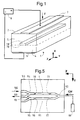
- Figure 1 shows a perspective view common to a first, a second and a third amplifiers and to a first, a second, and a third converters according to this invention.
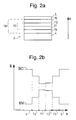
- Figures 2a, 3a and 4a respectively represent cross-sectional views of the chips semiconductors of these first, second and third amplifiers or converters according to this invention.
- Figures 2b, 3b and 4b show respectively energy level diagrams likely to be occupied by electrons at various dimensions above substrates of said chips of these amplifiers or converters, the energies of such levels being plotted on the ordinate, these dimensions being plotted on the abscissa.
- FIG. 5 represents a top view common to a fourth, a fifth and a sixth converter according to this invention.
- arrows indicate two say horizontal directions respectively constituting a longitudinal direction Z and a transverse direction Y.
- the so-called vertical direction DV has two meanings mutually opposite constituting an upward direction X and a direction down J. All of these directions are linked to a so-called semiconductor chip.
- This direct meaning is defined by the types of doping said lower and upper injection layers. It is such that this current injects charge carriers of the two so-called types in said active structure from of these injection layers.
- said active materials are included in said active structure 10 in the form of a plurality of homogeneous layers forming a succession in said vertical direction and constituting active layers, namely two such layers 11 and 12 in the case of the first object amplifier of the invention.
- This structure and these layers have respective thicknesses.
- These layers also have compositions defining respectively for these layers energy intervals, characteristic wavelengths, and gain bands, these gain bands of these layers partially overlapping each other.
- the realization of the active structure in the form of a limited number of homogeneous layers superimposed on each other has the advantage of being easier than in the form of a single thicker layer whose composition would gradually vary depending on the direction vertical.
- Each of said active layers offers amplification gains to said light waves when charge carriers of each of the two said types are present in this active layer with respective densities sufficient to allow these gains. These gains depend on the wavelengths of these waves. They are zero for the wavelengths outside the gain band of this layer.
- said gain band of the active structure is a composite gain band composed by said gain bands of said active layers. These gains also depend on the thicknesses and the positions of these layers. The thicknesses, positions and respective compositions of these active layers must then be chosen so that the same said pumping current can make appear in each of these layers and for each of the two said types of charge carriers a said density sufficient to allow a said gain for the wavelengths located in said gain band of this layer.
- said thicknesses of said active layers 11, 12 are between 20 and 400 nm, the number of these active layers is at most equal to four, and said respective energy intervals of any two of said active layers have a mutual difference at most equal to 60 meV.
- At least 80% of said core 10 of the guide of waves is constituted by said active layers.
- this core is constituted by said structure active, this means that these layers are more close to each other within this structure than quantum wells separated by barriers.
- More particularly said active layers 11, 12 are superimposed with contact between layers successive.
- Such proximity preferably ranging up to such contact, between active layers having increased refractive indices, i.e. higher to those of the surrounding layers, allows to give a high value at the confinement coefficient which represents the proportion in which the optical waves are confined to the active material. She favors thus the amplification action.
- the characteristic wavelengths of these layers containment are then external to said strip of composite gain and each of these confinement layers is in contact with a said active layer.
- All the layers of said waveguides have compositions corresponding to the formula Ga x In 1-x As y P 1-y .
- This provision is then constituted by the fact that said wavelength characteristic of said first active layer is smaller than that of said second active layer.
- Her goal is to increase the probability that the holes that are injected from the doped injection layer of the type p reach this second active layer. It is useful to achieve this goal because the probability has to be sufficient to allow said pumping current to maintain said sufficient density of these holes in this second active layer. It is reached thanks to fact that the relatively high energy interval of this first active layer gives a value relatively low the probability that these holes recombine with electrons during their course at through this first layer.
- said respective thicknesses of said active layers 11, 12 are between 50 and 200 nm approximately, said number of these active layers is at most equal to three, said difference between respective energy intervals of any two of these active layers is at most equal to 40 meV, and said pumping current has a surface intensity between 10 and 50 kA / cm2 approximately.
- At least said active layers are stressed enough to making a gain of said amplifier insensitive to a polarization of said optical waves traversing this guide.
- Such a constraint is used in known amplifiers to make the gain of an active layer insensitive to the possible polarization of optical waves propagating in this layer.
- Such insensitivity is sought in fiber optic communication networks because the waves received in a node of such a network at the outlet of a very long line most often have a polarization and because this polarization is random as to its degree and as to its direction.
- the desired stress is obtained by the choice of a suitable composition of the layer to be constrained because this choice makes it possible to give the crystalline mesh of the material of this layer a natural dimension different from that of the materials of the other layers of the semiconductor chip, this natural dimension being that which would appear in the absence of constraint.
- the crystalline continuity between the various layers of the chip then imposes on the mesh of the material of the layer to be constrained a modified dimension which is substantially equal to the natural dimension of the mesh of these other layers and this modification of dimension is accompanied by the realization of the desired constraint.
- the choice of the mesh size of a quaternary material having a chemical formula such as Ga x In 1-x As y P 1-y is compatible with the choice of the energy interval of this material despite the fact that these two choices are made through the composition of this material. This compatibility results from the presence in this formula of two parameters x and y which can be chosen independently of one another.
- the waveguide 18 of an amplifier according to this invention has a length of between 0.3 and 1 mm. This length is measured according to said longitudinal direction and it is typically equal to that of chip 2. The width of this guide is then typically between 1000 and 1500 nm.
- said active structure 10 is constituted by two layers which are a lower active layer 11 and an upper active layer 12 and which have the same thickness equal to 100 nm.
- the second and third amplifiers according to the present invention different from the first only by the constitution of their respective active structures, said confinement layers 24 and 25 of this second amplifier and 34 and 35 of this third amplifier being respectively identical to layers 14 and 15 previously described.
- This second amplifier has three layers active with the same thickness equal to 67 nm.
- That of a intermediate active layer 22 has the same composition as layer 12, a refractive index close to 3.5, and a characteristic wavelength of 1560 nm.
- Finally that of an upper active layer 23 has the same composition as layer 11, a refractive index close to 3.5 and a characteristic wavelength of 1530 nm.
- the third amplifier according to this invention also has three active layers.
- a lower active layer 31 has a thickness equal to 50 nm. Its composition is the same as that of the layer 11 and gives it a refractive index close to 3.5 and a characteristic wavelength of 1530 nm.
- An intermediate active layer 32 has a thickness equal to 100 nm. Its composition is the same as that of layer 12 and gives it a neighboring refractive index 3.5 and a characteristic wavelength of 1560 nm.
- the first, second and third said converters according to the present invention correspond first, second and third respectively amplifiers which have been described above.
- Each such converter includes a so-called semiconductor chip with said electrodes and said current source for supply this chip with its so-called pumping current, this chip not differing from the amplifier chip corresponding only by the length and width of said waveguide.
- the waveguide of such a converter presents typically a length between 1 and 4 mm and preferably between 1.5 and 2.5 mm, this length being measured in said longitudinal direction and being typically that of the chip of this converter.
- the width of this guide is typically between 1,000 and 1,500 nm.
- Such a converter performs intermodulation between the primary carrier wave and the reference wave. he may therefore be designated, to clarify the rest of the present description, by the designation "device intermodulation ".
- the fourth, fifth and sixth said converters according to this invention have such intermodulation devices. These last are identical to the first, second and third converters described above.
- the converter thus formed has the form of a Mach-Zehnder interferometer. How it works results from the fact that the secondary modulation includes a phase modulation. The latter is induced by modulation of the density of charge carriers which is caused by variations in the intensity of the wave primary carrier. It causes interference amplitude modulation of the output wave. This therefore requires balancing of respective intensities of the secondary carrier wave and of the amplified reference wave. This balancing is obtained by known means such as regulation of the intensity of the reference wave amplified by action on the pumping current of the amplifier reference. A fraction of this last wave can for that be taken out via a coupler auxiliary 95.
- Each of the converters described above comprises further an optical source 99 for supplying said wave auxiliary CW.
Landscapes
- Physics & Mathematics (AREA)
- Condensed Matter Physics & Semiconductors (AREA)
- General Physics & Mathematics (AREA)
- Electromagnetism (AREA)
- Optics & Photonics (AREA)
- Semiconductor Lasers (AREA)
- Optical Modulation, Optical Deflection, Nonlinear Optics, Optical Demodulation, Optical Logic Elements (AREA)
Abstract
Description
- Sa réalisation est complexe.
- L'obtention d'un gain souhaité dans chacune des bandes de gain des diverses couches actives exige que la circulation du courant de pompage crée une densité suffisante de porteurs de charge aussi bien positifs que négatifs dans chacune de ces couches. Cette exigence est facilement satisfaite pour les porteurs de charge négatifs constitués par les électrons parce que la grande mobilité de ces derniers leur permet d'atteindre rapidement les puits quantiques les plus éloignés de la couche d'injection de type n à partir de laquelle ils ont été injectés dans la structure active. Il n'en est malheureusement pas de même pour les porteurs de charge positifs constitués par des trous dont il est bien connu que la mobilité est bien moindre. Ces trous pourraient disparaitre en trop grand nombre par recombinaison dans les puits les plus proches de la couche d'injection de type p de laquelle ils proviennent, et par suite ne pas être injectés en nombre suffisant dans les puits les plus éloignés de cette couche. Il pourrait en résulter une insuffisance ou une trop grande instabilité du gain dans les bandes de gain des couches actives les plus proches de la couche d'injection de type n. Pour éviter qu'un tel défaut d'uniformité de l'injection de trous provoque une telle insuffisance ou instabilité du gain de certains puits, tous les puits quantiques et toutes les barrières de ce deuxième laser connu reçoivent un fort dopage de type p qui augmente artificiellement en tous points la densité des trous. Ce fort dopage présente l'inconvénient de compliquer encore la réalisation de l'amplificateur et surtout d'augmenter l'absorption de la lumière dans la structure active. Or une telle perte de lumière doit être compensée par une augmentation de l'intensité du courant de pompage ce qui provoque une augmentation correspondante de la puissance thermique à évacuer.
- Un substrat de phosphure d'indium à dopage de type n. Un tel substrat est couramment disponible dans le commerce.
- Ladite couche d'injection inférieure. Cette couche est constituée de phosphure d'indium. Elle a un dopage de type n et une concentration de dopage de 3.1018 cm-3. Le substrat et cette couche sont désignés collectivement sur la figure par la référence 4.
- Un guide d'ondes 18 s'étendant et guidant des ondes optiques selon la direction longitudinale Z et ayant une largeur limitée selon la direction transversale Y. Sur la figure 1 la puce 2 est supposée transparente pour permettre de voir ce guide. Les diverses couches constituant ce guide sont constituées de matériaux quaternaires, c'est à dire plus spécifiquement de phosphures et arséniures d'indium et de gallium. Elles n'ont aucun dopage intentionnel. Elle seront plus précisément décrites plus loin. De même que la couche d'injection inférieure elles ont été formées par des dépôts épitaxiaux successifs sur le substrat. Une gravure a ensuite délimité le guide selon la direction transversale avant le dépôt de la couche suivante. Ce guide d'ondes inclut une structure active 10 pour amplifier lesdites ondes optiques ayant des longueurs d'onde situées dans une bande de gain de cette structure. Cette structure est apte à amplifier ces ondes lorsque ces ondes se propagent dans cette structure en présence de porteurs de charges de chacun des deux types positif et négatif. Elle a un indice de réfraction moyen supérieur à des indices de réfraction de dites couches environnant cette structure pour constituer au moins une partie d'un coeur dudit guide d'ondes.
- Enfin ladite couche d'injection supérieure 5. Cette couche est constituée de phosphure d'indium. Elle a un dopage du type P et une concentration de dopage de 1018 cm-3.
- une électrode inférieure 6 formée sur ladite puce,
- une électrode supérieure 7 formée sur cette puce et coopérant avec ladite électrode inférieure pour permettre d'injecter un courant de pompage dans cette puce selon ladite direction verticale, et
- une source de courant 9 pour fournir ledit courant de pompage et pour l'injecter dans ladite puce dans un sens direct J constitué par l'un des deux dits sens de la direction verticale.
- l'intervalle énergétique local entre bande de valence et bande de conduction,
- la longueur d'onde caractéristique locale, et
- la position spectrale de la bande de gain locale.
Chacune des dites couches actives offre des gains d'amplification aux dites ondes lumineuses lorsque des porteurs de charge de chacun des deux dits types sont présents dans cette couche active avec des densités respectives suffisantes pour permettre ces gains. Ces gains dépendent des longueurs d'ondes de ces ondes. Ils sont nuls pour les longueurs d'onde extérieures à la bande de gain de cette couche. Il en résulte que ladite bande de gain de la structure active est une bande de gain composite composée par lesdites bandes de gain des dites couches actives. Ces gains dépendent aussi des épaisseurs et des positions de ces couches. Les épaisseurs, positions et compositions respectives de ces couches actives doivent alors être choisies pour qu'un même dit courant de pompage puisse faire apparaítre dans chacune de ces couches et pour chacun des deux dits types de porteurs de charges une dite densité suffisante pour permettre un dit gain pour les longueurs d'onde situées dans ladite bande de gain de cette couche.
- une couche de confinement inférieure 13 ayant un indice de réfraction et une longueur d'onde caractéristique respectivement inférieures à chacun desdits indices de réfraction et à chacune des dites longueurs d'onde caractéristiques des dites couches actives,
- ladite structure active 10, et
- une couche de confinement supérieure 14 ayant un indice de réfraction et une longueur d'onde caractéristique respectivement inférieures à chacun desdits indices de réfraction et à chacune des dites longueurs d'onde caractéristiques des dites couches actives.
- une première dite couche active 12 et
- une deuxième dite couche active 11.
- un port arrière 77 pour recevoir ladite onde auxiliaire CW sous la forme d'une onde continue dépourvue de modulation, et
- un port avant 78 pour recevoir ladite onde porteuse primaire SE et pour fournir ladite onde porteuse secondaire. Cette disposition est connue en elle même et elle est dite "contradirectionnelle" parce que l'onde porteuse primaire et l'onde auxiliaire circulent dans deux sens opposés. Elle permet notamment d'allouer une même longueur d'onde à ces deux ondes lorsque cela est utile.
- ledit dispositif d'intermodulation 1,
- un amplificateur de référence 91 sensiblement identique à ce dispositif d'intermodulation et constitué d'éléments ayant respectivement des mêmes fonctions et des mêmes dénominations que des éléments correspondants de ce dispositif, et
- des guides d'ondes optiques constituant :
- un coupleur en Y constituant un coupleur arrière 92 pour recevoir une onde ayant la longueur d'onde souhaitée pour ladite onde auxiliaire CW et pour transmettre deux parties égales de cette onde respectivement audit port arrière 77 dudit dispositif d'intermodulation pour constituer ladite onde auxiliaire et au port arrière 97 correspondant dudit amplificateur de référence pour constituer une onde de référence et pour que cette onde de référence soit transformée par cet amplificateur de référence en une onde de référence amplifiée, et
- un coupleur avant composite comportant :
- un coupleur en Y constituant un coupleur de sortie 93 pour recevoir la dite onde porteuse secondaire à partir dudit port avant 78 dudit dispositif d'intermodulation et ladite onde de référence amplifiée à partir du port avant 98 correspondant dudit amplificateur de référence et pour fournir en sortie dudit convertisseur une onde de sortie SS constituée par la réunion et par l'interférence de cette onde porteuse secondaire et de cette onde de référence amplifiée, et
- un coupleur en Y constituant un coupleur d'entrée 94 pour recevoir ladite onde porteuse primaire en entrée dudit convertisseur et pour la transmettre audit port avant (78) dudit dispositif d'intermodulation.
Claims (21)
- Composant optique à semiconducteur, ce composant comportant un guide d'ondes (18) faisant partie d'une puce semiconductrice (2) constituée de couches s'étendant selon des directions horizontales (Y,Z) de cette puce et formant une succession présentant une continuité cristalline selon une direction verticale (X) de cette puce, ce guide d'ondes s'étendant selon une dite direction horizontale (Z) et incluant des matériaux actifs (11, 12), ces matériaux ayant des compositions et des intervalles énergétiques respectifs les rendant aptes à amplifier des ondes optiques se propageant dans ce guide, ces matériaux présentant selon ladite direction verticale une variation de composition entrainant une variation d'intervalle énergétique,
ce composant étant caractérisé par le fait que certains au moins desdits matériaux actifs sont inclus dans ledit guide d'ondes sous la forme de matériaux massifs. - Composant optique selon la revendication 1, ce composant constituant un amplificateur optique, ladite direction verticale (DV) ayant deux sens mutuellement opposés constituant un sens vers le haut (X) et un sens vers le bas (J), ladite succession de couches incluant dans ledit sens vers le haut:ledit amplificateur comportant en outre :une couche d'injection inférieure (4) ayant un dopage d'un premier type de conductivité,une structure active (10) incluant les dits matériaux actifs pour amplifier des dites ondes optiques ayant des longueurs d'onde situées dans une bande de gain de cette structure, cette structure étant apte à amplifier ces ondes lorsque ces ondes se propagent dans cette structure en présence de porteurs de charges de chacun des deux types positif et négatif, cette structure ayant un indice de réfraction moyen supérieur à des indices de réfraction de dites couches environnant cette structure pour constituer au moins une partie d'un coeur dudit guide d'ondes (18), etune couche d'injection supérieure (5) ayant un dopage du deuxième type de conductivité,ledit amplificateur étant caractérisé par le fait que lesdits matériaux actifs sont inclus dans ladite structure active (10) sous la forme d'une pluralité de couches homogènes formant une succession selon ladite direction verticale et constituant respectivement des couches actives (11, 12), cette structure et ces couches ayant des épaisseurs respectives, ces couches ayant aussi des compositions définissant respectivement pour ces couches des intervalles énergétiques, des longueurs d'ondes caractéristiques, et des bandes de gain, ces bandes de gain de ces couches se recouvrant partiellement les unes les autres, chacune de ces couches actives offrant des gains d'amplification aux dites ondes optiques lorsque à la fois les longueurs d'ondes de ces ondes sont comprises dans la bande de gain de cette couche et des porteurs de charge de chacun des deux dits types sont présents dans cette couche active avec des densités respectives suffisantes pour permettre ces gains, grâce à quoi ladite bande de gain de la structure active est une bande de gain composite composée par lesdites bandes de gain des dites couches actives.une électrode inférieure (6) formée sur ladite puce,une électrode supérieure (7) formée sur cette puce et coopérant avec ladite électrode inférieure pour permettre d'injecter un courant de pompage dans cette puce selon ladite direction verticale, etune source de courant (9) pour fournir ledit courant de pompage et pour l'injecter dans ladite puce dans un sens direct (J) constitué par l'un des deux dits sens de la direction verticale, ce sens direct étant défini par les dits types de dopages des dites couches d'injection et étant tel que ce courant injecte des porteurs de charge des deux dits types dans ladite structure active à partir de ces couches d'injection,
- Amplificateur optique selon la revendication 2, cet amplificateur étant caractérisé par le fait que lesdites épaisseurs des dites couches actives (11, 12) sont comprises entre 20 et 400 nm, le nombre de ces couches actives étant au plus égal à quatre, lesdits intervalles énergétiques respectifs de deux quelconques des dites couches actives présentant une différence mutuelle au plus égale à 60 meV.
- Amplificateur optique selon la revendication 3, cet amplificateur étant caractérisé par le fait qu'au moins 80% du volume dudit coeur (10) dudit guides d'ondes est constituée par lesdites couches actives.
- Amplificateur optique selon la revendication 4 cet amplificateur étant caractérisé par le fait que lesdites couches actives (11, 12) sont superposées avec contact entre couches successives.
- Amplicateur optique selon la revendication 5, cet amplificateur étant caractérisé par le fait que ladite succession de couches inclut selon ladite direction verticale dans ledit sens vers le haut (X) :lesdites longueurs d'onde caractéristiques des couches de confinement étant extérieures à ladite bande de gain composite, chacune de ces couches de confinement étant en contact avec une dite couche active.ladite couche d'injection inférieure (4),une couche de confinement inférieure (13) ayant un indice de réfraction et une longueur d'onde caractéristique, respectivement inférieures à chacun desdits indices de réfraction et à chacune des dites longueurs d'onde caractéristiques des dites couches actives,ladite structure active (10),une couche de confinement supérieure (14) ayant un indice de réfraction et une longueur d'onde caractéristique respectivement inférieures à chacun desdits indices de réfraction et à chacune des dites longueurs d'onde caractéristiques des dites couches actives, etladite couche d'injection supérieure (5),
- Amplificateur optique selon la revendication 6, amplificateur dans lequel ladite structure active (10) inclut successivement selon ladite direction verticale dans ledit sens direct (J) :cet amplificateur étant caractérisé par le fait que ladite longueur d'onde caractéristique de ladite première couche active est plus petite que celle de ladite deuxième couche active.une première dite couche active (12), etune deuxième dite couche active (11),
- Amplificateur optique selon la revendication 3, cet amplificateur étant caractérisé par le fait que les dites épaisseurs respectives des dites couches actives (11, 12) sont comprises entre 50 et 200 nm environ, ledit nombre de ces couches actives étant au plus égal à trois, ladite différence entre les intervalles énergétiques respectifs de deux quelconques de ces couches actives étant au plus égale à 40 meV, ledit courant de pompage ayant une intensité surfaçique comprise entre 10 et 50 kA/cm2 environ.
- Amplificateur optique selon la revendication 6, cet amplificateur étant caractérisé par le fait que les dites couches d'injection inférieure (4) et supérieure (5) sont constituées d'un composé semiconducteur binaire du type III-V, les dites couches actives (11, 12) et les dites couches de confinement (14, 15) étant constituées de composés quaternaires du type arséniure et phosphure d'indium et de gallium avec des proportions respectives de l'arsénic par rapport au phosphore et de l'indium par rapport au gallium, ces couches actives et de confinement étant dépourvues de dopage intentionnel.
- Amplificateur optique selon la revendication 2, cet amplificateur étant caractérisé par le fait que, parmi celles des dites couches qui constituent ledit guide d'ondes (18), au moins lesdites couches actives subissent une contrainte suffisante pour rendre un gain dudit amplificateur insensible à une polarisation des dites ondes optiques parcourant ce guide.
- Amplificateur optique selon la revendication 2, cet amplificateur étant caractérisé par le fait que ledit guide d'ondes (18) présente une longueur comprise entre 0,3 et 1 mm.
- Composant selon la revendication 1, ce composant constituant un convertisseur de longueur d'onde optique, ce convertisseur comportant des moyens pour permettre audit guide d'ondes (18) de guider en même temps deux ondes optiques constituant respectivement une onde porteuse primaire(SE) et une onde auxiliaire (CW), cette onde porteuse ayant une longueur d'onde primaire et ayant une modulation d'amplitude portant un signal à transmettre et constituant une modulation primaire, ce guide d'onde incluant une structure active (10) sensible à ladite modulation primaire pour transformer ladite onde auxiliaire en une onde porteuse secondaire ayant une même longueur d'onde que cette onde auxiliaire tout en ayant une modulation secondaire portant ledit signal à transmettre,
ledit convertisseur de longueur d'onde optique étant caractérisé par le fait que ladite structure active inclut une pluralité de matériaux actifs (11, 12) sensibles chacun à ladite modulation primaire seulement lorsque ladite longueur d'onde est comprise dans une bande spectrale constituant une bande de gain de ce matériau actif, les dites bandes de gain de ces matériaux actifs étant décalées les unes par rapport aux autres. - Convertisseur de longueur d'onde optique selon la revendication 12, ce convertisseur étant caractérisé par le fait que ladite pluralité de matériaux actifs est incluse dans ladite structure active (10) sous la forme de matériaux massifs.
- Convertisseur de longueur d'onde optique selon la revendication 13, ce convertisseur étant caractérisé par le fait que lesdits matériaux actifs (11, 12) constituent au moins pour partie un coeur (10) dudit guide d'ondes (18) et occupent au moins 80% de ce coeur.
- Convertisseur de longueur d'onde optique selon la revendication 13, ce convertisseur étant caractérisé par le fait que ladite pluralité de matériaux actifs est incluse dans ladite structure active (10) sous la forme d'une pluralité de couches homogènes constituées respectivement par ces matériaux actifs et constituant respectivement des couches actives (11, 12), ces couches actives étant superposées les unes aux autres.
- Convertisseur de longueur d'onde optique selon la revendication 15, ce convertisseur étant caractérisé par le fait que lesdites couches actives (11,12) sont superposées avec contact des unes avec les autres.
- Convertisseur de longueurs d'onde optique selon la revendication 12, ledit guide d'ondes (18) de ce convertisseur s'étendant selon une direction longitudinale (Z) entre :ledit convertisseur étant caractérisé par le fait qu'il est conforme à un amplificateur optique selon l'une quelconque des revendications 2 à 10, ladite puce semiconductrice, ledit guide d'ondes et ladite structure active de cet amplificateur constituant en même temps respectivement ladite puce semiconductrice (2), ledit guide d'ondes (18) et ladite structure active (10) de ce convertisseur, ce convertisseur constituant un dispositif d'intermodulation (1).un port arrière (77) pour recevoir ladite onde auxiliaire (CW) sous la forme d'une onde continue dépourvue de modulation, etun port avant (78) pour recevoir ladite onde porteuse primaire (SE) et pour fournir ladite onde porteuse secondaire,
- Convertisseur de longueur d'onde optique selon la revendication 17, ce convertisseur étant caractérisé par le fait que ledit guide d'ondes (18) présente selon ladite direction longitudinale (Z) une longueur comprise entre 1 et 4 mm.
- Convertisseur selon la revendication 18, ce convertisseur étant caractérisé par le fait que ladite longueur dudit guide d'ondes (18) est comprise entre 1,5 et 2,5 mm.
- Convertisseur de longueur d'onde optique selon la revendication 17, ce convertisseur étant caractérisé par le fait qu'il comporte une base (90) et, sur cette base :ledit dispositif d'intermodulation (1),un amplificateur de référence (91) sensiblement identique à ce dispositif d'intermodulation et constitué d'éléments ayant respectivement des mêmes fonctions et des mêmes dénominations que des éléments correspondants de ce dispositif d'intermodulation, etdes guides d'ondes optiques constituant :un coupleur en Y constituant un coupleur arrière (92) pour recevoir une onde ayant la longueur d'onde souhaitée pour ladite onde auxiliaire (CW) et pour transmettre deux parties égales de cette onde respectivement audit port arrière (77) dudit dispositif d'intermodulation pour constituer ladite onde auxiliaire et au port arrière (97) correspondant dudit amplificateur de référence pour constituer une onde de référence et pour que cette onde de référence soit transformée par cet amplificateur de référence en une onde de référence amplifiée, etun coupleur avant composite comportant :un coupleur en Y constituant un coupleur de sortie (93) pour recevoir la dite onde porteuse secondaire à partir dudit port avant (78) dudit dispositif d'intermodulation et ladite onde de référence amplifiée à partir du port avant (98) correspondant dudit amplificateur de référence et pour fournir en sortie dudit convertisseur une onde de sortie (SS) constituée par la réunion et par l'interférence de cette onde porteuse secondaire et de cette onde de référence amplifiée, etun coupleur en Y constituant un coupleur d'entrée (94) pour recevoir ladite onde porteuse primaire en entrée dudit convertisseur et pour la transmettre audit port avant (78) dudit dispositif d'intermodulation.
- Convertisseur de longueur d'onde optique selon l'une quelconque des revendications 12 à 20, ce convertisseur comportant en outre une source optique (99) pour fournir ladite onde auxiliaire (CW).
Applications Claiming Priority (2)
| Application Number | Priority Date | Filing Date | Title |
|---|---|---|---|
| FR9807493A FR2779838B1 (fr) | 1998-06-15 | 1998-06-15 | Composant optique a semiconducteur et amplificateur et convertisseur de longueurs d'onde constitues par ce composant |
| FR9807493 | 1998-06-15 |
Publications (1)
| Publication Number | Publication Date |
|---|---|
| EP0966078A1 true EP0966078A1 (fr) | 1999-12-22 |
Family
ID=9527375
Family Applications (1)
| Application Number | Title | Priority Date | Filing Date |
|---|---|---|---|
| EP99401448A Withdrawn EP0966078A1 (fr) | 1998-06-15 | 1999-06-14 | Composant optique à semiconducteur et amplificateur et convertisseur de longueurs d'onde constitués par ce composant |
Country Status (5)
| Country | Link |
|---|---|
| US (1) | US6271961B1 (fr) |
| EP (1) | EP0966078A1 (fr) |
| JP (1) | JP2000012984A (fr) |
| CA (1) | CA2272834A1 (fr) |
| FR (1) | FR2779838B1 (fr) |
Families Citing this family (9)
| Publication number | Priority date | Publication date | Assignee | Title |
|---|---|---|---|---|
| JP2001053392A (ja) * | 1999-06-03 | 2001-02-23 | Fujitsu Ltd | 偏波無依存型半導体光増幅器 |
| JP3038383B1 (ja) * | 1999-06-08 | 2000-05-08 | 東京大学長 | 光デバイス |
| KR100301067B1 (ko) * | 1999-08-23 | 2001-11-01 | 윤종용 | 마이크로 스크래치 검사방법 및 이를 적용한 장치 |
| US6636318B2 (en) | 2000-10-06 | 2003-10-21 | Alphion Corp. | Bit-rate and format insensitive all-optical circuit for reshaping, regeneration and retiming of optical pulse streams |
| US6563621B2 (en) | 2000-10-06 | 2003-05-13 | Alphion Corporation | Bit-rate and format insensitive all-optical clock extraction circuit |
| WO2006104935A2 (fr) * | 2005-03-28 | 2006-10-05 | Goldeneye,Inc. | Diodes electroluminescentes et procedes de fabrication associes |
| US7319555B2 (en) * | 2005-04-27 | 2008-01-15 | Alphion Corporation | Integrated performance monitoring, performance maintenance, and failure detection for photonic regenerators |
| US7319518B2 (en) * | 2005-08-24 | 2008-01-15 | Cree, Inc. | Double side polished wafer scratch inspection tool |
| JP2010121291A (ja) * | 2008-11-17 | 2010-06-03 | Noda Corp | 床材 |
Citations (5)
| Publication number | Priority date | Publication date | Assignee | Title |
|---|---|---|---|---|
| US4680769A (en) * | 1984-11-21 | 1987-07-14 | Bell Communications Research, Inc. | Broadband laser amplifier structure |
| US5283799A (en) * | 1991-02-27 | 1994-02-01 | Alcatel N.V. | Semiconductor laser with a saturable absorber |
| WO1996009668A1 (fr) * | 1994-09-14 | 1996-03-28 | British Telecommunications Public Limited Company | Dispositif optique |
| JPH08334797A (ja) * | 1995-06-07 | 1996-12-17 | Oki Electric Ind Co Ltd | 光波長変換集積素子 |
| US5754714A (en) * | 1994-09-17 | 1998-05-19 | Kabushiki Kaisha Toshiba | Semiconductor optical waveguide device, optical control type optical switch, and wavelength conversion device |
Family Cites Families (1)
| Publication number | Priority date | Publication date | Assignee | Title |
|---|---|---|---|---|
| JP3195159B2 (ja) * | 1993-11-25 | 2001-08-06 | 株式会社東芝 | 光半導体素子 |
-
1998
- 1998-06-15 FR FR9807493A patent/FR2779838B1/fr not_active Expired - Fee Related
-
1999
- 1999-05-21 CA CA002272834A patent/CA2272834A1/fr not_active Abandoned
- 1999-05-25 US US09/318,273 patent/US6271961B1/en not_active Expired - Fee Related
- 1999-06-14 EP EP99401448A patent/EP0966078A1/fr not_active Withdrawn
- 1999-06-14 JP JP11167464A patent/JP2000012984A/ja active Pending
Patent Citations (5)
| Publication number | Priority date | Publication date | Assignee | Title |
|---|---|---|---|---|
| US4680769A (en) * | 1984-11-21 | 1987-07-14 | Bell Communications Research, Inc. | Broadband laser amplifier structure |
| US5283799A (en) * | 1991-02-27 | 1994-02-01 | Alcatel N.V. | Semiconductor laser with a saturable absorber |
| WO1996009668A1 (fr) * | 1994-09-14 | 1996-03-28 | British Telecommunications Public Limited Company | Dispositif optique |
| US5754714A (en) * | 1994-09-17 | 1998-05-19 | Kabushiki Kaisha Toshiba | Semiconductor optical waveguide device, optical control type optical switch, and wavelength conversion device |
| JPH08334797A (ja) * | 1995-06-07 | 1996-12-17 | Oki Electric Ind Co Ltd | 光波長変換集積素子 |
Non-Patent Citations (1)
| Title |
|---|
| PATENT ABSTRACTS OF JAPAN vol. 097, no. 004 30 April 1997 (1997-04-30) * |
Also Published As
| Publication number | Publication date |
|---|---|
| JP2000012984A (ja) | 2000-01-14 |
| US6271961B1 (en) | 2001-08-07 |
| CA2272834A1 (fr) | 1999-12-15 |
| FR2779838A1 (fr) | 1999-12-17 |
| FR2779838B1 (fr) | 2000-08-04 |
Similar Documents
| Publication | Publication Date | Title |
|---|---|---|
| EP0742620B1 (fr) | Laser à semiconducteurs | |
| EP0829934B1 (fr) | Procédé de fabrication d'un composant optoélectronique à semiconducteur et composant ou matrice de composants fabriqués selon ce procédé | |
| EP0575227B1 (fr) | Procédé et dispositif de modulation et d'amplification de faisceaux lumineux | |
| EP0527060A1 (fr) | Emetteur-récepteur optique à semiconducteurs | |
| EP0667660A1 (fr) | Laser à réflecteurs de Bragg distribués, accordable en longueur d'onde, à réseaux de diffraction virtuels actives sélectivement | |
| FR2493616A1 (fr) | Laser a injection a heterostructure | |
| FR2495383A1 (fr) | Diode electroluminescente a superradiance ayant un rendement de couplage eleve avec un guide d'ondes optiques | |
| FR2765347A1 (fr) | Reflecteur de bragg en semi-conducteur et procede de fabrication | |
| EP0966078A1 (fr) | Composant optique à semiconducteur et amplificateur et convertisseur de longueurs d'onde constitués par ce composant | |
| FR2695761A1 (fr) | Procédé de fabrication de dispositifs électro-optiques à ruban, notamment de lasers, et dispositifs ainsi obtenus. | |
| EP0823982B1 (fr) | Amplificateur optique a semi-conducteur | |
| EP1138101B1 (fr) | Laser de type semi-conducteur | |
| EP0752743A1 (fr) | Dispositif laser à structure enterrée pour circuit photonique intégré et procédé de fabrication | |
| EP0306400B1 (fr) | Modulateur pour onde électromagnétique, à puits quantiques, et utilisation de ce modulateur comme polariseur | |
| EP0252565B1 (fr) | Dispositif semiconducteur intégré du type dispositif de couplage entre un photodéecteur et un guide d'ond lumineuse | |
| EP0828325A1 (fr) | Amplificateur optique à semi-conducteur | |
| FR2845833A1 (fr) | Amplificateur optique a semiconducteurs a stabilisation de gain laterale et distribuee | |
| EP0993088A1 (fr) | Laser à semiconducteur, à spectre de gain accordable | |
| EP0992842B1 (fr) | Dispositif de régénération d'un signal multiplexé en longueurs d'onde comprenant un absorbant saturable | |
| EP0664588B1 (fr) | Structure semiconductrice à réseau de diffraction virtuel | |
| FR2790837A1 (fr) | Systeme optoelectronique comprenant plusieurs sections a fonctions respectives couplees par couplage evanescent et procede de realisation | |
| WO2000022704A1 (fr) | Procede de controle d'un laser semiconducteur unipolaire | |
| FR2786279A1 (fr) | Composant optique a base d'amplificateurs optiques a semi-conducteur comportant un nombre reduit d'electrodes independantes | |
| FR2635418A1 (fr) | Laser a emission de surface a signaux lumineux combines | |
| FR2673342A1 (fr) | Dispositif a retroaction positive pour le traitement d'un signal optique. |
Legal Events
| Date | Code | Title | Description |
|---|---|---|---|
| PUAI | Public reference made under article 153(3) epc to a published international application that has entered the european phase |
Free format text: ORIGINAL CODE: 0009012 |
|
| AK | Designated contracting states |
Kind code of ref document: A1 Designated state(s): DE GB IT SE |
|
| AX | Request for extension of the european patent |
Free format text: AL;LT;LV;MK;RO;SI |
|
| 17P | Request for examination filed |
Effective date: 20000623 |
|
| AKX | Designation fees paid |
Free format text: DE GB IT SE |
|
| RAP1 | Party data changed (applicant data changed or rights of an application transferred) |
Owner name: AVANEX CORPORATION |
|
| RIC1 | Information provided on ipc code assigned before grant |
Ipc: 7G 02F 2/00 B Ipc: 7H 01S 5/10 A |
|
| RIC1 | Information provided on ipc code assigned before grant |
Ipc: 7G 02F 2/00 B Ipc: 7H 01S 5/10 A |
|
| GRAP | Despatch of communication of intention to grant a patent |
Free format text: ORIGINAL CODE: EPIDOSNIGR1 |
|
| STAA | Information on the status of an ep patent application or granted ep patent |
Free format text: STATUS: THE APPLICATION IS DEEMED TO BE WITHDRAWN |
|
| 18D | Application deemed to be withdrawn |
Effective date: 20050104 |