EP0966112A1 - Verfahren und System zur Induktive Koplung Detektion von einem Belastungsmodulationssignal - Google Patents
Verfahren und System zur Induktive Koplung Detektion von einem Belastungsmodulationssignal Download PDFInfo
- Publication number
- EP0966112A1 EP0966112A1 EP99111698A EP99111698A EP0966112A1 EP 0966112 A1 EP0966112 A1 EP 0966112A1 EP 99111698 A EP99111698 A EP 99111698A EP 99111698 A EP99111698 A EP 99111698A EP 0966112 A1 EP0966112 A1 EP 0966112A1
- Authority
- EP
- European Patent Office
- Prior art keywords
- signal
- coil
- circuit
- phase
- antenna
- Prior art date
- Legal status (The legal status is an assumption and is not a legal conclusion. Google has not performed a legal analysis and makes no representation as to the accuracy of the status listed.)
- Granted
Links
Images


Classifications
-
- G—PHYSICS
- G06—COMPUTING OR CALCULATING; COUNTING
- G06K—GRAPHICAL DATA READING; PRESENTATION OF DATA; RECORD CARRIERS; HANDLING RECORD CARRIERS
- G06K19/00—Record carriers for use with machines and with at least a part designed to carry digital markings
-
- H—ELECTRICITY
- H04—ELECTRIC COMMUNICATION TECHNIQUE
- H04B—TRANSMISSION
- H04B5/00—Near-field transmission systems, e.g. inductive or capacitive transmission systems
- H04B5/20—Near-field transmission systems, e.g. inductive or capacitive transmission systems characterised by the transmission technique; characterised by the transmission medium
- H04B5/22—Capacitive coupling
-
- H—ELECTRICITY
- H04—ELECTRIC COMMUNICATION TECHNIQUE
- H04B—TRANSMISSION
- H04B5/00—Near-field transmission systems, e.g. inductive or capacitive transmission systems
- H04B5/40—Near-field transmission systems, e.g. inductive or capacitive transmission systems characterised by components specially adapted for near-field transmission
- H04B5/48—Transceivers
-
- H—ELECTRICITY
- H04—ELECTRIC COMMUNICATION TECHNIQUE
- H04B—TRANSMISSION
- H04B5/00—Near-field transmission systems, e.g. inductive or capacitive transmission systems
- H04B5/20—Near-field transmission systems, e.g. inductive or capacitive transmission systems characterised by the transmission technique; characterised by the transmission medium
- H04B5/24—Inductive coupling
- H04B5/26—Inductive coupling using coils
- H04B5/266—One coil at each side, e.g. with primary and secondary coils
-
- H—ELECTRICITY
- H04—ELECTRIC COMMUNICATION TECHNIQUE
- H04B—TRANSMISSION
- H04B5/00—Near-field transmission systems, e.g. inductive or capacitive transmission systems
- H04B5/70—Near-field transmission systems, e.g. inductive or capacitive transmission systems specially adapted for specific purposes
- H04B5/73—Near-field transmission systems, e.g. inductive or capacitive transmission systems specially adapted for specific purposes for taking measurements, e.g. using sensing coils
Definitions
- the present invention relates to a method and a detection system by inductive coupling of a signal load modulation emitted by a modulation system charge.
- the present invention relates in particular to reception of binary data sent by a circuit integrated operating without contact, for example a circuit integrated in a contactless smart card, a electronic tag, an electronic token ...
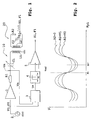
- Figure 1 shows the diagram electric system with a detection system 10 and a load modulation system 20 cooperating by coupling inductive.
- the system 10 includes an adjustable capacity C1 and coil L1 in series forming a resonant circuit.
- the capacity C1 is connected via a resistance R1 at the output of an amplifier voltage / current 1 receiving a voltage as input alternative V0 of frequency F0, delivered by a oscillator 2.
- the voltage V0 converted into current by amplifier 1, forms the excitation signal of the resonant circuit L1C1 whose natural frequency Fp1 is set in the vicinity of the excitation frequency F0.
- the detection system load modulation 20 includes an antenna coil L2 forming with a capacity C2 a resonant circuit of natural frequency Fp2 tuned to frequency F0.
- the coil L2 is connected in parallel with means of load modulation, here an R2 resistor in series with a Tm switch.
- the Tm switch is controlled by a signal S1 of binary type, of carrier frequency F1, to be detected by the system 10.
- the modulations of load applied to coil L2 according to fluctuations of signal S1 are reflected by coupling inductive on coil L1, and we observe across the antenna circuit L1C1 an alternating voltage Vm of frequency F0, amplitude and phase modulated.
- the detection of the modulation signal load S1 is provided by a phase 3 comparator receiving as input the voltages V0 and Vm.
- the comparator 3 delivers a voltage V ⁇ proportional to the phase shift of these two signals.
- the voltage V ⁇ is filtered by a bandpass 4 set on the carrier frequency F1 of the signal S1.
- the output of bandpass 4 is made binary by a comparator 5 with threshold Vref. At the output of comparator 5, there is the signal S1 of frequency F1.
- an objective of the present invention is to provide a system and a method for detecting load modulation by phase comparison which does not does not have the disadvantages of the method described above.
- this objective is achieved by a method of detecting a load modulation signal received by inductive coupling in an antenna circuit comprising a detection coil excited by a signal of predetermined frequency, comprising a step of comparison of the phase of the excitation signal of the coil with the phase of a signal taken from the circuit antenna, method in which the antenna circuit does not not form a resonant circuit near the frequency of the excitation signal, and the phase of the excitation signal with the phase of the current crossing the detection coil.
- the detection coil and the coil of the integrated circuit are respectively formed by primary and secondary windings of a transformer, the secondary winding being connected to the pads of the integrated circuit.
- the present invention also relates to a system detection by inductive coupling of a signal load modulation, including an antenna circuit comprising a coil, means for applying to the antenna circuit a frequency excitation signal predetermined, phase comparator means receiving on a first input the excitation signal and on a second input a signal taken from the circuit antenna, and means for extracting the signal from load modulation of a phase signal delivered by the comparator means, in which: the antenna circuit does not form a resonant circuit near the frequency of the excitation signal, and the means phase comparators receive on their second input a signal delivered by current detection means crossing the coil.
- the means of current detection include a transformer whose the primary winding is connected in series with the antenna coil.
- the secondary of transformer is connected in parallel with a resistance, to convert current into voltage crossing the primary.
- the means for extract the load modulation signal include a bandpass filter centered on a carrier frequency of the load modulation signal.
- the present invention also relates to a data receiving station by inductive coupling and load modulation, including a detection system according to the invention for detecting a modulation signal load, and a decoder circuit for extracting load modulation signal data.
- the present invention also relates to a integrated circuit test station operating without contact by means of an antenna coil, comprising a detection system according to the invention for detecting a load modulation signal emitted by the circuit integrated.
- the system coil and the coil of the integrated circuit are primary and secondary windings of a transformer.
- the station comprises a decoder circuit for extracting data from the signal load modulation detected.
- Figure 3 shows, in its left part, a detection system 30 according to the invention of a signal load modulation.
- a detection system 30 according to the invention of a signal load modulation.
- the most of the elements described in the preamble, including the references are kept, except for the capacity C1 which is deleted.
- the system 30 differs indeed of that of FIG. 1 by the fact that the circuit antenna, which here includes only the coil L1, does not not form a resonant circuit near the frequency F0 of the excitation signal V0.
- phase 3 comparator delivering the phase signal V ⁇ receives the signal as input excitation V0 and a signal V (Im) which is the image of the current Im passing through coil L1.
- the signal V (Im) is delivered by a current sensor 31 here taking the form of a transformer having primary windings 31-1 and secondary 31-2.
- Primary winding 31-1 does not here has only one turn and is connected in series with coil L1.
- Secondary winding 31-2 is connected in parallel with a conversion resistance Ri current / voltage.
- phase 3 comparator is made of simple way using two clipping circuits 3-1, 3-2 whose exits attack the entrances of a door logic 3-3 of the EXCLUSIVE OR type, the phase signal V ⁇ being delivered through gate 3-3.
- the phase 3 comparator is connected to a bandpass filter 4 followed by a comparator 5 at threshold Vref.
- the advantage of the system 30 according to the invention is that it does not require any adjustment of its antenna circuit while providing excellent signal sensitivity phase V ⁇ to load modulations. This result is obtained by the combination of the two characteristics described above, namely the forecast of a circuit antenna not resonant at frequency F0 and neighboring frequencies, and a phase comparison based on detection of the antenna current Im.
- Figure 3 also illustrates an application of the system 30 upon reception of data transmitted by a integrated circuit IC operating without contact, including electrical diagram is shown on the right side of the figure.
- the IC circuit is equipped with the antenna coil L2, the capacitor C2, the resistor R2 and the switch load modulation Tm described in the preamble. At the terminals coil L2, appears an alternating induced voltage Vac of frequency F0, image of the voltage Vm present at coil L1 terminals.
- the integrated circuit IC also includes a encoder circuit CD, a data memory MEM, a MP microprocessor, a DIV frequency divider circuit and a Pd diode bridge arranged to rectify the voltage Vac.
- the DIV circuit delivers to the CD encoder circuit a clock signal extracted from the voltage Vac, the frequency F1 is a sub-multiple of frequency F0.
- the CD circuit for example a BPSK encoder by jumps of phase, receives digital data DT from memory MEM and delivers the load modulation signal S1, from carrier frequency F1.
- the rectifier Pd delivers a direct voltage Vcc ensuring the supply electrical circuit IC.
- the DT data to be transmitted is injected under coded form in the load modulation signal S1.
- the system output 30 is applied to the input of a DEC decoder which demodulates the signal S1 and extracts the digital data DT.
- the integrated circuit IC can be arranged in a portable medium such as a plastic card, a token, a label ...
- the detection system 30 forms thus, with the DEC decoder, a receiving station 50 data, for example a smart card reader without contact.
- Station 50 may include means for send data to integrated circuit IC, for example means for modulating the signal amplitude excitation V0. Such means are well known to skilled in the art and will not be described here in a concern for simplicity.
- the detection system according to the invention is intended to operate with a strong inductive coupling between the coils L1 and L2.
- the current invention is thus reserved for applications with low communication distance, for example to readers of contactless cards with an entry slot and a map guide. Such readers guarantee short communication distance, on the order of a few millimeters.
- the present invention is also applicable to the creation of a test station for testing a contactless integrated circuit before assembly on a support and its connection to an antenna coil. According to a aspect of the present invention, it is proposed to simulate the antenna coil L2 of the integrated circuit by means of the secondary winding of a transformer whose the primary winding forms the coil L1 of the detection 30.
- FIG. 4 shows schematically such a test station 60.
- Station 60 includes a transformer TR, the detection system 30 according to the invention, the DEC decoder already described and a unit control unit 61 receiving the DT data delivered by the DEC circuit.
- the primary winding T1 of the transformer TR forms the coil of the detection system 30.
- the secondary winding T2 is connected via of electrical wires 62 to metal spikes 63.64 fixed on a printed circuit board 65.
- the tips 63, 64 are applied to pads 41, 42 of the circuit integrated IC intended to be soldered to a coil antenna.
- the winding T2 forms a coil dummy antenna for operating and test the IC circuit before mounting it on a support portable and its connection to an antenna coil.
- This aspect of the invention guarantees a strong coupling inductive between the T1 and T2 windings and allows build a low maintenance test station, do not requiring no adjustment of its antenna circuit and can be arranged in a production line of integrated circuits. Integrated circuits can be tested while they are still collectively present on a silicon wafer, or "wafer", before the cutting of the mother wafer.
Landscapes
- Engineering & Computer Science (AREA)
- Computer Networks & Wireless Communication (AREA)
- Signal Processing (AREA)
- Physics & Mathematics (AREA)
- General Physics & Mathematics (AREA)
- Theoretical Computer Science (AREA)
- Near-Field Transmission Systems (AREA)
Applications Claiming Priority (2)
| Application Number | Priority Date | Filing Date | Title |
|---|---|---|---|
| FR9807678 | 1998-06-18 | ||
| FR9807678A FR2780222B1 (fr) | 1998-06-18 | 1998-06-18 | Procede et systeme de detection par couplage inductif d'un signal de modulation de charge |
Publications (2)
| Publication Number | Publication Date |
|---|---|
| EP0966112A1 true EP0966112A1 (de) | 1999-12-22 |
| EP0966112B1 EP0966112B1 (de) | 2001-11-21 |
Family
ID=9527533
Family Applications (1)
| Application Number | Title | Priority Date | Filing Date |
|---|---|---|---|
| EP99111698A Expired - Lifetime EP0966112B1 (de) | 1998-06-18 | 1999-06-17 | Verfahren und System zur Detektion eines Belastungsmodulationssignals durch induktive Kopplung |
Country Status (4)
| Country | Link |
|---|---|
| US (1) | US6329808B1 (de) |
| EP (1) | EP0966112B1 (de) |
| DE (1) | DE69900622T2 (de) |
| FR (1) | FR2780222B1 (de) |
Cited By (1)
| Publication number | Priority date | Publication date | Assignee | Title |
|---|---|---|---|---|
| EP2506185A1 (de) | 2011-03-29 | 2012-10-03 | Pollux | Funkkommunikationsverfahren mit Erfassung der Präsenz eines RFID-Chips, und System zur Umsetzung eines solchen Verfahrens |
Families Citing this family (61)
| Publication number | Priority date | Publication date | Assignee | Title |
|---|---|---|---|---|
| FR2814242B1 (fr) * | 2000-09-19 | 2002-12-20 | France Telecom | Dispositif de mesure ponctuelle d'un champ magnetique radiofrequence d'amplitude et de frequence constantes |
| FR2815490B1 (fr) * | 2000-10-16 | 2006-07-07 | Inside Technologies | Lecteur de circuit integre sans contact |
| WO2002101952A1 (en) * | 2001-06-12 | 2002-12-19 | Main.Net Communications Ltd. | Coupling circuits for power line communications |
| GB0208449D0 (en) * | 2002-04-10 | 2002-05-22 | Zarlink Semiconductor Ab | Method of saving power in RF devices |
| US7088145B2 (en) * | 2002-12-23 | 2006-08-08 | 3M Innovative Properties Company | AC powered logic circuitry |
| FR2851382B1 (fr) * | 2003-02-14 | 2008-07-11 | Baracoda | Systeme a module de communication bluetooth a alimentation commandee, ensemble de radiocommunication, procedes et lecteurs |
| DE10329655A1 (de) * | 2003-07-01 | 2005-02-03 | Infineon Technologies Ag | Elektronisches Bauelement |
| US7078937B2 (en) * | 2003-12-17 | 2006-07-18 | 3M Innovative Properties Company | Logic circuitry powered by partially rectified ac waveform |
| US7508686B2 (en) * | 2005-06-29 | 2009-03-24 | Sigmatel, Inc. | System and method for configuring direct current converter |
| US11881814B2 (en) | 2005-12-05 | 2024-01-23 | Solaredge Technologies Ltd. | Testing of a photovoltaic panel |
| US10693415B2 (en) | 2007-12-05 | 2020-06-23 | Solaredge Technologies Ltd. | Testing of a photovoltaic panel |
| US8013472B2 (en) | 2006-12-06 | 2011-09-06 | Solaredge, Ltd. | Method for distributed power harvesting using DC power sources |
| US8384243B2 (en) | 2007-12-04 | 2013-02-26 | Solaredge Technologies Ltd. | Distributed power harvesting systems using DC power sources |
| US11735910B2 (en) | 2006-12-06 | 2023-08-22 | Solaredge Technologies Ltd. | Distributed power system using direct current power sources |
| US8963369B2 (en) | 2007-12-04 | 2015-02-24 | Solaredge Technologies Ltd. | Distributed power harvesting systems using DC power sources |
| US8319483B2 (en) | 2007-08-06 | 2012-11-27 | Solaredge Technologies Ltd. | Digital average input current control in power converter |
| US11855231B2 (en) | 2006-12-06 | 2023-12-26 | Solaredge Technologies Ltd. | Distributed power harvesting systems using DC power sources |
| US11309832B2 (en) | 2006-12-06 | 2022-04-19 | Solaredge Technologies Ltd. | Distributed power harvesting systems using DC power sources |
| US8947194B2 (en) | 2009-05-26 | 2015-02-03 | Solaredge Technologies Ltd. | Theft detection and prevention in a power generation system |
| US11569659B2 (en) | 2006-12-06 | 2023-01-31 | Solaredge Technologies Ltd. | Distributed power harvesting systems using DC power sources |
| US9088178B2 (en) | 2006-12-06 | 2015-07-21 | Solaredge Technologies Ltd | Distributed power harvesting systems using DC power sources |
| US8319471B2 (en) | 2006-12-06 | 2012-11-27 | Solaredge, Ltd. | Battery power delivery module |
| US8816535B2 (en) | 2007-10-10 | 2014-08-26 | Solaredge Technologies, Ltd. | System and method for protection during inverter shutdown in distributed power installations |
| US11687112B2 (en) | 2006-12-06 | 2023-06-27 | Solaredge Technologies Ltd. | Distributed power harvesting systems using DC power sources |
| US11888387B2 (en) | 2006-12-06 | 2024-01-30 | Solaredge Technologies Ltd. | Safety mechanisms, wake up and shutdown methods in distributed power installations |
| US11296650B2 (en) * | 2006-12-06 | 2022-04-05 | Solaredge Technologies Ltd. | System and method for protection during inverter shutdown in distributed power installations |
| US12316274B2 (en) | 2006-12-06 | 2025-05-27 | Solaredge Technologies Ltd. | Pairing of components in a direct current distributed power generation system |
| US8473250B2 (en) | 2006-12-06 | 2013-06-25 | Solaredge, Ltd. | Monitoring of distributed power harvesting systems using DC power sources |
| US8618692B2 (en) | 2007-12-04 | 2013-12-31 | Solaredge Technologies Ltd. | Distributed power system using direct current power sources |
| US8049523B2 (en) | 2007-12-05 | 2011-11-01 | Solaredge Technologies Ltd. | Current sensing on a MOSFET |
| EP3496258B1 (de) | 2007-12-05 | 2025-02-05 | Solaredge Technologies Ltd. | Sicherheitsmechanismus in verteilten strominstallationen |
| US11264947B2 (en) | 2007-12-05 | 2022-03-01 | Solaredge Technologies Ltd. | Testing of a photovoltaic panel |
| EP2294669B8 (de) | 2008-05-05 | 2016-12-07 | Solaredge Technologies Ltd. | Gleichstrom-leistungskombinierer |
| US12418177B2 (en) | 2009-10-24 | 2025-09-16 | Solaredge Technologies Ltd. | Distributed power system using direct current power sources |
| CN105939030B (zh) * | 2010-01-25 | 2019-06-18 | 飞利浦知识产权企业有限公司 | 用于检测经无线电力链路的数据通信的系统和方法 |
| GB2508548B (en) * | 2010-01-25 | 2014-08-13 | Access Business Group Int Llc | Systems and methods for detecting data communication over a wireless power link |
| US10673222B2 (en) | 2010-11-09 | 2020-06-02 | Solaredge Technologies Ltd. | Arc detection and prevention in a power generation system |
| GB2485527B (en) | 2010-11-09 | 2012-12-19 | Solaredge Technologies Ltd | Arc detection and prevention in a power generation system |
| US10230310B2 (en) | 2016-04-05 | 2019-03-12 | Solaredge Technologies Ltd | Safety switch for photovoltaic systems |
| US10673229B2 (en) | 2010-11-09 | 2020-06-02 | Solaredge Technologies Ltd. | Arc detection and prevention in a power generation system |
| US9397729B2 (en) | 2010-11-15 | 2016-07-19 | Taiwan Semiconductor Manufacturing Company, Ltd. | Through chip coupling for signal transport |
| JP5750031B2 (ja) * | 2010-11-19 | 2015-07-15 | 株式会社半導体エネルギー研究所 | 電子回路及び半導体装置 |
| US9106269B2 (en) | 2010-12-08 | 2015-08-11 | Access Business Group International Llc | System and method for providing communications in a wireless power supply |
| GB2483317B (en) | 2011-01-12 | 2012-08-22 | Solaredge Technologies Ltd | Serially connected inverters |
| JP6001563B2 (ja) * | 2011-02-07 | 2016-10-05 | アクセス ビジネス グループ インターナショナル リミテッド ライアビリティ カンパニー | 無線電力伝送システムで通信を提供するシステム及び方法 |
| KR101218989B1 (ko) * | 2011-07-15 | 2013-01-21 | 삼성전기주식회사 | 반도체 패키지 및 그 제조방법 |
| US8570005B2 (en) | 2011-09-12 | 2013-10-29 | Solaredge Technologies Ltd. | Direct current link circuit |
| GB2498365A (en) | 2012-01-11 | 2013-07-17 | Solaredge Technologies Ltd | Photovoltaic module |
| US9853565B2 (en) | 2012-01-30 | 2017-12-26 | Solaredge Technologies Ltd. | Maximized power in a photovoltaic distributed power system |
| GB2498790A (en) | 2012-01-30 | 2013-07-31 | Solaredge Technologies Ltd | Maximising power in a photovoltaic distributed power system |
| GB2498791A (en) | 2012-01-30 | 2013-07-31 | Solaredge Technologies Ltd | Photovoltaic panel circuitry |
| GB2499991A (en) | 2012-03-05 | 2013-09-11 | Solaredge Technologies Ltd | DC link circuit for photovoltaic array |
| US9287827B2 (en) * | 2012-09-06 | 2016-03-15 | Qualcomm Incorporated | System and method to demodulate a load modulated signal |
| US9548619B2 (en) | 2013-03-14 | 2017-01-17 | Solaredge Technologies Ltd. | Method and apparatus for storing and depleting energy |
| EP3174454B1 (de) | 2014-07-30 | 2019-02-20 | The Alfred E. Mann Foundation for Scientific Research | Drahtlose energieübertragung und kommunikation |
| CN105429307B (zh) * | 2015-11-26 | 2019-02-22 | 南京南瑞集团公司 | 无线信号能量收集方法、无线传感器唤醒方法及其装置 |
| US11018623B2 (en) | 2016-04-05 | 2021-05-25 | Solaredge Technologies Ltd. | Safety switch for photovoltaic systems |
| US12057807B2 (en) | 2016-04-05 | 2024-08-06 | Solaredge Technologies Ltd. | Chain of power devices |
| US11177663B2 (en) | 2016-04-05 | 2021-11-16 | Solaredge Technologies Ltd. | Chain of power devices |
| JP6690609B2 (ja) * | 2017-04-06 | 2020-04-28 | 株式会社村田製作所 | 磁界発生回路 |
| FR3098908A1 (fr) * | 2019-07-19 | 2021-01-22 | Continental Automotive Gmbh | Capteur sans contact pour véhicule automobile |
Citations (3)
| Publication number | Priority date | Publication date | Assignee | Title |
|---|---|---|---|---|
| US4928087A (en) * | 1988-03-25 | 1990-05-22 | Angewandte Digital Electronik Gmbh | Phase-stabilized, phase-coupled resonant circuit |
| EP0492569A2 (de) * | 1990-12-28 | 1992-07-01 | On Track Innovations Ltd. | System und Verfahren zur kontaktlosen Datenübertragung |
| EP0704928A2 (de) * | 1994-09-30 | 1996-04-03 | Hughes Identification Devices, Inc. | HF Transpondersystem mit Parallelresonanz-Abfrage und Serienresonanz-Antwort |
Family Cites Families (4)
| Publication number | Priority date | Publication date | Assignee | Title |
|---|---|---|---|---|
| DE3402737C1 (de) * | 1984-01-27 | 1985-08-01 | Angewandte Digital Elektronik Gmbh, 2051 Brunstorf | Vorrichtung zur gegenseitigen Informationsuebertragung |
| US4654658A (en) * | 1984-08-03 | 1987-03-31 | Walton Charles A | Identification system with vector phase angle detection |
| US5343079A (en) * | 1991-02-25 | 1994-08-30 | Regents Of The University Of Minnesota | Standby power supply with load-current harmonics neutralizer |
| US5717722A (en) * | 1994-11-08 | 1998-02-10 | Anritsu Corporation | Precision symbol demodulation system for multi-carrier modulation signal |
-
1998
- 1998-06-18 FR FR9807678A patent/FR2780222B1/fr not_active Expired - Fee Related
-
1999
- 1999-06-03 US US09/325,188 patent/US6329808B1/en not_active Expired - Lifetime
- 1999-06-17 EP EP99111698A patent/EP0966112B1/de not_active Expired - Lifetime
- 1999-06-17 DE DE69900622T patent/DE69900622T2/de not_active Expired - Lifetime
Patent Citations (3)
| Publication number | Priority date | Publication date | Assignee | Title |
|---|---|---|---|---|
| US4928087A (en) * | 1988-03-25 | 1990-05-22 | Angewandte Digital Electronik Gmbh | Phase-stabilized, phase-coupled resonant circuit |
| EP0492569A2 (de) * | 1990-12-28 | 1992-07-01 | On Track Innovations Ltd. | System und Verfahren zur kontaktlosen Datenübertragung |
| EP0704928A2 (de) * | 1994-09-30 | 1996-04-03 | Hughes Identification Devices, Inc. | HF Transpondersystem mit Parallelresonanz-Abfrage und Serienresonanz-Antwort |
Cited By (1)
| Publication number | Priority date | Publication date | Assignee | Title |
|---|---|---|---|---|
| EP2506185A1 (de) | 2011-03-29 | 2012-10-03 | Pollux | Funkkommunikationsverfahren mit Erfassung der Präsenz eines RFID-Chips, und System zur Umsetzung eines solchen Verfahrens |
Also Published As
| Publication number | Publication date |
|---|---|
| EP0966112B1 (de) | 2001-11-21 |
| FR2780222A1 (fr) | 1999-12-24 |
| FR2780222B1 (fr) | 2000-08-11 |
| DE69900622D1 (de) | 2002-01-31 |
| DE69900622T2 (de) | 2002-08-01 |
| US6329808B1 (en) | 2001-12-11 |
Similar Documents
| Publication | Publication Date | Title |
|---|---|---|
| EP0966112B1 (de) | Verfahren und System zur Detektion eines Belastungsmodulationssignals durch induktive Kopplung | |
| US6650226B1 (en) | Detection, by an electromagnetic transponder reader, of the distance separating it from a transponder | |
| EP1568130B1 (de) | Abstimmbare antennenschaltung, insbesondere für ein kontaktloses integriertes lesegerät | |
| EP1042731B1 (de) | Kontaktchipkarte/kontaktlose chipkarte mit abänderungsfähiger antennenschnittstelle | |
| EP1045325B1 (de) | Entfernungsbestimmung zwischen einem elektromagnetischen Transponder und einem Terminal | |
| EP1312032B1 (de) | Hochempfindlicher leser für passive transponder | |
| WO1998026371A1 (fr) | Systeme d'echange de donnees a communication par contacts ou sans contact entre une borne et des objets portatifs | |
| EP0290547A1 (de) | Identifikationssystem. | |
| EP1043677B1 (de) | Ein mit sehr naher Koppelung arbeitendes Lesegerät für elektromagnetische Transponder | |
| EP1043680A1 (de) | Enggekoppelter elektromagnetischer Transponder | |
| EP0903689A1 (de) | Demodulator für kontaktlose Chipkarte | |
| KR100411562B1 (ko) | Ask-복조 방법 및 ask-복조기 | |
| EP1369813B1 (de) | Lesegerät für einen elektromagnetischen Transponder | |
| EP1043679B1 (de) | Leser mit Einrichtung zur Bestimmung des Abstandes zwischen dem Leser und einem Transponder | |
| EP0525642B1 (de) | Lese/Schreibsystem für Aufzeichnungsmedium und kontaktfreies IC-Karten-System | |
| US7215723B2 (en) | Demodulator for an amplitude-modulated alternating signal | |
| EP1446765B1 (de) | Empfängerschaltung und methode für ein kontaktloses identifikationssystem | |
| FR2782209A1 (fr) | Objet portatif telealimente pour la communication sans contact par voie inductive avec une borne | |
| US7756223B2 (en) | Contactless data carrier with current demodulation | |
| EP0468848B1 (de) | Elektrischer Verbinder für Chipkarten und Vorrichtung und Anwendung zur Betrugsdetektion unter Anwendung dieses Verbinders | |
| EP0910905A1 (de) | Vorrichtung zum senden und empfangen von digitalen daten durch elektromagnetische induktion und induktive ankopplung | |
| FR2814242A1 (fr) | Dispositif de mesure ponctuelle d'un champ magnetique radiofrequence d'amplitude et de frequence constantes | |
| JP3065169B2 (ja) | 非接触型icカード | |
| JP2004348661A (ja) | 非接触式icカード | |
| JP2006270699A (ja) | 非接触型id識別装置 |
Legal Events
| Date | Code | Title | Description |
|---|---|---|---|
| PUAI | Public reference made under article 153(3) epc to a published international application that has entered the european phase |
Free format text: ORIGINAL CODE: 0009012 |
|
| AK | Designated contracting states |
Kind code of ref document: A1 Designated state(s): AT BE CH CY LI |
|
| AX | Request for extension of the european patent |
Free format text: AL;LT;LV;MK;RO;SI |
|
| 17P | Request for examination filed |
Effective date: 20000504 |
|
| AKX | Designation fees paid |
Free format text: AT BE CH CY LI |
|
| RBV | Designated contracting states (corrected) |
Designated state(s): DE FR GB IT |
|
| REG | Reference to a national code |
Ref country code: DE Ref legal event code: 8566 |
|
| GRAG | Despatch of communication of intention to grant |
Free format text: ORIGINAL CODE: EPIDOS AGRA |
|
| 17Q | First examination report despatched |
Effective date: 20010202 |
|
| GRAG | Despatch of communication of intention to grant |
Free format text: ORIGINAL CODE: EPIDOS AGRA |
|
| GRAH | Despatch of communication of intention to grant a patent |
Free format text: ORIGINAL CODE: EPIDOS IGRA |
|
| GRAG | Despatch of communication of intention to grant |
Free format text: ORIGINAL CODE: EPIDOS AGRA |
|
| GRAH | Despatch of communication of intention to grant a patent |
Free format text: ORIGINAL CODE: EPIDOS IGRA |
|
| GRAH | Despatch of communication of intention to grant a patent |
Free format text: ORIGINAL CODE: EPIDOS IGRA |
|
| GRAA | (expected) grant |
Free format text: ORIGINAL CODE: 0009210 |
|
| AK | Designated contracting states |
Kind code of ref document: B1 Designated state(s): DE FR GB IT |
|
| PG25 | Lapsed in a contracting state [announced via postgrant information from national office to epo] |
Ref country code: IT Free format text: LAPSE BECAUSE OF FAILURE TO SUBMIT A TRANSLATION OF THE DESCRIPTION OR TO PAY THE FEE WITHIN THE PRE;WARNING: LAPSES OF ITALIAN PATENTS WITH EFFECTIVE DATE BEFORE 2007 MAY HAVE OCCURRED AT ANY TIME BEFORE 2007. THE CORRECT EFFECTIVE DATE MAY BE DIFFERENT FROM THE ONE RECORDED.SCRIBED TIME-LIMIT Effective date: 20011121 |
|
| GBT | Gb: translation of ep patent filed (gb section 77(6)(a)/1977) |
Effective date: 20011122 |
|
| RAP2 | Party data changed (patent owner data changed or rights of a patent transferred) |
Owner name: STMICROELECTRONICS S.A. |
|
| REG | Reference to a national code |
Ref country code: GB Ref legal event code: IF02 |
|
| REF | Corresponds to: |
Ref document number: 69900622 Country of ref document: DE Date of ref document: 20020131 |
|
| PLBE | No opposition filed within time limit |
Free format text: ORIGINAL CODE: 0009261 |
|
| STAA | Information on the status of an ep patent application or granted ep patent |
Free format text: STATUS: NO OPPOSITION FILED WITHIN TIME LIMIT |
|
| 26N | No opposition filed | ||
| PGFP | Annual fee paid to national office [announced via postgrant information from national office to epo] |
Ref country code: GB Payment date: 20080527 Year of fee payment: 10 |
|
| GBPC | Gb: european patent ceased through non-payment of renewal fee |
Effective date: 20090617 |
|
| PG25 | Lapsed in a contracting state [announced via postgrant information from national office to epo] |
Ref country code: GB Free format text: LAPSE BECAUSE OF NON-PAYMENT OF DUE FEES Effective date: 20090617 |
|
| PGFP | Annual fee paid to national office [announced via postgrant information from national office to epo] |
Ref country code: FR Payment date: 20100729 Year of fee payment: 12 Ref country code: DE Payment date: 20100610 Year of fee payment: 12 |
|
| REG | Reference to a national code |
Ref country code: FR Ref legal event code: ST Effective date: 20120229 |
|
| REG | Reference to a national code |
Ref country code: DE Ref legal event code: R119 Ref document number: 69900622 Country of ref document: DE Effective date: 20120103 |
|
| PG25 | Lapsed in a contracting state [announced via postgrant information from national office to epo] |
Ref country code: FR Free format text: LAPSE BECAUSE OF NON-PAYMENT OF DUE FEES Effective date: 20110630 Ref country code: DE Free format text: LAPSE BECAUSE OF NON-PAYMENT OF DUE FEES Effective date: 20120103 |