EP0966165A1 - Circuit de traitement de signal video délivrant un niveau de signal optimal pour la correction inverse de gamma - Google Patents
Circuit de traitement de signal video délivrant un niveau de signal optimal pour la correction inverse de gamma Download PDFInfo
- Publication number
- EP0966165A1 EP0966165A1 EP99110983A EP99110983A EP0966165A1 EP 0966165 A1 EP0966165 A1 EP 0966165A1 EP 99110983 A EP99110983 A EP 99110983A EP 99110983 A EP99110983 A EP 99110983A EP 0966165 A1 EP0966165 A1 EP 0966165A1
- Authority
- EP
- European Patent Office
- Prior art keywords
- primary color
- video signals
- analog
- level
- circuit
- Prior art date
- Legal status (The legal status is an assumption and is not a legal conclusion. Google has not performed a legal analysis and makes no representation as to the accuracy of the status listed.)
- Granted
Links
Images


Classifications
-
- H—ELECTRICITY
- H04—ELECTRIC COMMUNICATION TECHNIQUE
- H04N—PICTORIAL COMMUNICATION, e.g. TELEVISION
- H04N9/00—Details of colour television systems
- H04N9/64—Circuits for processing colour signals
- H04N9/68—Circuits for processing colour signals for controlling the amplitude of colour signals, e.g. automatic chroma control circuits
- H04N9/69—Circuits for processing colour signals for controlling the amplitude of colour signals, e.g. automatic chroma control circuits for modifying the colour signals by gamma correction
-
- G—PHYSICS
- G09—EDUCATION; CRYPTOGRAPHY; DISPLAY; ADVERTISING; SEALS
- G09G—ARRANGEMENTS OR CIRCUITS FOR CONTROL OF INDICATING DEVICES USING STATIC MEANS TO PRESENT VARIABLE INFORMATION
- G09G2320/00—Control of display operating conditions
- G09G2320/02—Improving the quality of display appearance
- G09G2320/0271—Adjustment of the gradation levels within the range of the gradation scale, e.g. by redistribution or clipping
-
- G—PHYSICS
- G09—EDUCATION; CRYPTOGRAPHY; DISPLAY; ADVERTISING; SEALS
- G09G—ARRANGEMENTS OR CIRCUITS FOR CONTROL OF INDICATING DEVICES USING STATIC MEANS TO PRESENT VARIABLE INFORMATION
- G09G3/00—Control arrangements or circuits, of interest only in connection with visual indicators other than cathode-ray tubes
- G09G3/20—Control arrangements or circuits, of interest only in connection with visual indicators other than cathode-ray tubes for presentation of an assembly of a number of characters, e.g. a page, by composing the assembly by combination of individual elements arranged in a matrix no fixed position being assigned to or needed to be assigned to the individual characters or partial characters
Definitions
- the present invention relates to a video signal processing circuit having an inverse gamma correcting circuit for effecting an inverse gamma correction to three primary color input video signals or three primary color digital video signals, respectively.
- Gamma correction is commonly effected to a video signal.
- a signal processing circuit When processing such a video signal by a signal processing circuit and displaying the processed signal on a display apparatus, it is general to use an inverse gamma correcting circuit for performing a correction opposite to the gamma correction provided in the signal processing circuit.
- Figure 1 shows the structure of a video signal processing circuit conventionally used for displaying video signals onto a plasma display panel (hereinafter, referred to as PDP).
- An analog luminance signal Y and first and second analog color difference signals (B-Y) and (R-Y) indicative of the video signals are supplied to a matrix circuit 1 by which analog three primary color video signals of red (R), green (G), and blue (B) are generated.
- the analog three primary color video signals RGB are supplied to analog/digital converters (hereinafter, referred to as A/D converters) 3r, 3g, and 3b and are converted to digital signals having a predetermined number of bits, respectively.
- A/D converters analog/digital converters
- the three primary color digital video signals are supplied to inverse gamma correcting circuits 4r, 4g, and 4b wherein the input signals are processed by an inverse gamma correction operation, thereby substantially linear three primary color video signals Rout, Gout, and Bout are produced.
- the three primary color video signals are then supplied to the PDP and an image corresponding to the video signals is displayed.
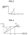
- characteristics of the output signals are as shown in Fig. 2 with respect to the three primary color digital video signals RGB supplied to the inverse gamma correcting circuits 4r, 4g, and 4b. That is, the output signal characteristics with respect to the input three primary color digital video signals are in the form of characteristics of an exponential function or characteristics which are approximate to them.
- the dynamic range will be a range from "0" to "Da” which is smaller than 100% of the broadest range. In this way, a reduction of dynamic range occurs. Consequently, it becomes difficult to obtain desired contrast. In such a case, the luminance of the screen will be reduced to render the whole screen dark, so that it also makes difficult to obtain desired brightness characteristics.
- the invention has been made in view of the above problems and an object of the invention is to provide a video signal processing circuit which can produce a signal having a dynamic range extended nearly to 100% of its capability, so that a desired contrast can be obtained, and desired brightness characteristics can be obtained by an increase in the maximum luminance of the screen.
- a video signal processing circuit having inverse gamma correcting circuits for effecting an inverse gamma correction to three primary color input video signals according to three primary color video signals of red, green, and blue carrying video information, comprising: peak level detecting means for detecting a peak level of each of the three primary color video signals; and a level control circuit for controlling a signal level of each of the three primary color input video signals which are supplied to the inverse gamma correcting circuits in accordance with the detected peak levels, wherein the level control circuit performs a control operation in which the level of each of the three primary color input video signals which are supplied to the inverse gamma correcting circuits equals a peak value when the peak levels are equal to or larger than a predetermined value.
- the level control circuit performs a control operation in which, when the peak levels are equal to or less than the predetermined value, the three primary color input video signals which are supplied to the inverse gamma correcting circuits are set to signal levels obtained by multiplying the three primary color video signals of red, green, and blue carrying the video information by a predetermined coefficient of "1" or more.
- a video signal processing circuit comprising: a gain control amplifier which amplifies analog three primary color video signals of red, green, and blue indicative of video information by a predetermined gain and in which the gain is controlled by a gain control signal; analog/digital converter for converting the analog three primary color video signals which are generated from the gain control amplifier into digital signals; inverse gamma correcting circuits for effecting an inverse gamma correction to the three primary color digital video signals; a peak level detecting circuit for detecting a peak level of each of the analog three primary color video signals which are supplied to the analog/digital converters; and a gain control signal generator for generating the gain control signal in accordance with the detected peak levels, wherein the gain control signal generator generates the gain control signal to control the gain control amplifier so that when the peak level is equal to or larger than a predetermined value, a level of each of the three primary color digital video signals which are generated from the analog/digital converters is set to the peak value.
- the gain control signal generator when the peak level is equal to or less than the predetermined value, the gain control signal generator generates the gain control signal so that the gain control amplifier amplifies the analog three primary color video signals by a predetermined gain of "1" or more.
- a video signal processing circuit comprising: a matrix circuit to which an analog luminance signal and first and second analog color difference signals indicative of video information are supplied and which generates analog three primary color video signals of red, green, and blue; analog/digital converters for converting the analog three primary color video signals into digital signals; inverse gamma correcting circuits for effecting an inverse gamma correction to the three primary color digital video signals; a peak level detecting circuit for detecting a peak level of each of the analog three primary color video signals; and a level control circuit for controlling a signal level of the analog luminance signal in accordance with the detected peak level, wherein the level control circuit performs a control operation in which, when the peak level is equal to a predetermined value or more, the level of each of the three primary color digital video signals which are generated by the analog/digital converters is set to a peak value.
- the level control circuit when the peak level is equal to or less than the predetermined value, performs a control operation in which the analog three primary color video signals which are supplied to the analog/digital converters is set to a signal level obtained by multiplying the analog luminance signal by a predetermined coefficient of "1" or more.
- FIG. 3 shows an example of the structure of a signal processing circuit according to the invention.
- Analog three primary color video signals of red (R), green (G), and blue (B) which are generated from the matrix circuit 1 are supplied to an RGB amplifier 2 as a gain control amplifier and are amplified by a predetermined gain, so that analog three primary color video signals Ra, Ga, and Ba are generated.
- the gain of the RGB amplifier 2 is controlled by a gain control signal which is generated from a gain control signal generator 8.
- the analog three primary color video signals Ra, Ga, and Ba generated from the RGB amplifier 2 are converted into digital signals by the A/D converters 3r, 3g, and 3b, and are processed by an inverse gamma correction at the inverse gamma correcting circuits 4r, 4g, and 4b, respectively.
- the analog three primary color video signals Ra, Ga, and Ba from the RGB amplifier 2 are supplied to low pass filters (hereinafter, referred to as LPFs) 5r, 5g, and 5b, respectively.
- LPFs low pass filters
- the OR of the signals passed through the LPFs is generated by an OR circuit 6.
- An output from the OR circuit 6 is supplied to a peak holding circuit 7, by which a peak value of the OR output is held.
- the peak value is supplied to the gain control signal generator 8 and a gain control signal according to the peak value is generated.
- the gain of the RGB amplifier 2 is controlled by the gain control signal.
- the analog three primary color video signals Ra, Ga, and Ba from the RGB amplifier 2 pass through the LPFs 5r, 5g, and 5b, thereby preventing that peak voltages at leading and trailing edges of the video signals which are caused by an outline correcting circuit are not generated. That is, a process for emphasizing the outline of the video signal is generally performed by the outline correcting circuit at the front stage of the present processing circuit. For example, the leading or trailing waveform of the video signal is projected by differentiating the video signal, thereby emphasizing the outline.
- the signal at the leading or trailing edge is regarded as a peak of the video signal and is held by the peak holding circuit 7, the peak levels of the analog three primary color video signals Ra, Ga, and Ba cannot be correctly detected, so that the contrast cannot be accurately controlled.
- the three primary color video signals Ra, Ga, and Ba By allowing the three primary color video signals Ra, Ga, and Ba to pass through the LPFs 5r, 5g, and 5b, the emphasized waveform due to the outline correcting circuit is blocked.
- the OR of the outputs from the LPFs 5r, 5g, and 5b is obtained by the OR circuit 6 and the signal having the maximum level among the analog three primary color video signals Ra, Ga, and Ba is generated.
- This signal is held by the peak holding circuit 7 for a predetermined period (for example, a period of time of several fields) and the peak level of the analog three primary color video signals Ra, Ga, and Ba is held.
- the gain control signal generator 8 generates the gain control signal in accordance with the peak level, thereby controlling the gain of the RGB amplifier 2.
- FIG. 4 shows characteristics of the input signal which is supplied to each of the A/D converters 3r, 3g, and 3b for a signal level of an input video signal (Y).
- Characteristics (a) denote characteristics according to the processing circuit of the invention and characteristics (b) indicate characteristics according to the conventional circuit shown in Fig. 1.
- the three primary color signals R, G, and B which are supplied from the matrix circuit 1 to the A/D converters 3r, 3g, and 3b for the input video signals become linear characteristics.
- the input video signal level reaches a predetermined value (120 in Fig. 4)
- the outputs from the A/D converters 3r, 3g, and 3b reach a peak value.
- the signal level (input of the A/D converter) of each of the three primary color signals R, G, and B is set to 100.
- the peak value is equal to "255".
- the characteristics are as shown in a range shown by a hatched portion in Fig. 4, so that the A/D conversion output is saturated and a crushed image having no gradation is displayed.
- the characteristics (a) indicate characteristics according to the processing circuit of the invention.
- the peak value in the three primary color signals Ra, Ga, and Ba according to the input signal level that is obtained by the peak holding circuit 7 is compared with a preset predetermined reference value Vref by the gain control signal generator 8.
- the gain control signal is generated so that the RGB amplifier 2 has a predetermined gain larger than 1 (gain > 1).
- the three primary color signals R, G, and B are amplified by the same gain, thereby generating the signals Ra, Ga, and Ba.
- the gain of the RGB amplifier 2 is set by the gain control signal so that the outputs of the A/D converters 3r, 3g, and 3b are equal to the peak value by the input signals (Ra, Ga, Ba) of the A/D converters 3r, 3g, and 3b.
- the signal of each of the A/D converters 3r, 3g, and 3b is constituted by 8 bits, as mentioned above, the peak value of the output is equal to "255", so that the peak value "255" is generated by the input signals ("100") of the A/D converters 3r, 3g, and 3b.
- the gain of the RGB amplifier 2 is decreased and the signal levels of the input signals (Ra, Ga, Ba) are limited so that the outputs of the A/D converters 3r, 3g, and 3b are always equal to the peak value (for example, "255"), thereby maintaining the levels constant.
- the outputs of the A/D converters 3r, 3g, and 3b are always equal to the peak value.
- the signal levels which are supplied to the inverse gamma correcting circuits 4r, 4g, and 4b at the post stage, consequently, are set to Db in Fig. 2 and the input signal level lies within a range of "0" to "the peak value", for example, in a range of "0" to "255” so long as the signal of each of the A/D converters 3r, 3g, and 3b is constituted by 8 bits, so that 100% of the dynamic range is utilized.
- the predetermined reference value Vref can be set to a fixed value or can be also manually varied by the user. In this case, when the user adjusts the contrast, the reference value Vref can be varied.
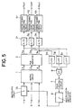
- FIG. 5 shows another embodiment according to the invention and the same reference numerals as those in Fig. 1 denote the same component elements.
- the luminance signal Y representing the input video signal is supplied to the matrix circuit 1 through a multiplying circuit 10.
- a multiplication coefficient generator 9 generates a multiplication coefficient which is sent to the multiplying circuit 10 in accordance with the peak value from the peak holding circuit 7.
- the peak value in the three primary color signals Ra, Ga, and Ba is compared with the predetermined reference value Vref by the multiplication coefficient generator 9.
- a predetermined multiplication coefficient larger than 1 (multiplication coefficient > 1) is generated and supplied to the multiplying circuit 10.
- the luminance signal Y is multiplied by the multiplication coefficient by the multiplying circuit 10 and the resultant signal is supplied to the matrix circuit 1.
- the display apparatus which is applied to the invention is not limited to the PDP. So long as the signal processing circuit in the display apparatus has the inverse gamma correcting circuit, the invention can also be applied to the other display apparatus by liquid crystal or a CRT.
- Desired brightness characteristics can be also obtained by an increase in the maximum luminance of the screen.
Landscapes
- Engineering & Computer Science (AREA)
- Multimedia (AREA)
- Signal Processing (AREA)
- Processing Of Color Television Signals (AREA)
- Picture Signal Circuits (AREA)
- Control Of Indicators Other Than Cathode Ray Tubes (AREA)
- Control Of Gas Discharge Display Tubes (AREA)
Applications Claiming Priority (2)
| Application Number | Priority Date | Filing Date | Title |
|---|---|---|---|
| JP10189922A JP2000013814A (ja) | 1998-06-19 | 1998-06-19 | 映像信号処理回路 |
| JP18992298 | 1998-06-19 |
Publications (2)
| Publication Number | Publication Date |
|---|---|
| EP0966165A1 true EP0966165A1 (fr) | 1999-12-22 |
| EP0966165B1 EP0966165B1 (fr) | 2006-05-17 |
Family
ID=16249463
Family Applications (1)
| Application Number | Title | Priority Date | Filing Date |
|---|---|---|---|
| EP99110983A Expired - Lifetime EP0966165B1 (fr) | 1998-06-19 | 1999-06-09 | Circuit de traitement de signal video délivrant un niveau de signal optimal pour la correction inverse de gamma |
Country Status (5)
| Country | Link |
|---|---|
| US (1) | US6271891B1 (fr) |
| EP (1) | EP0966165B1 (fr) |
| JP (1) | JP2000013814A (fr) |
| CN (1) | CN1263314C (fr) |
| DE (1) | DE69931308T2 (fr) |
Cited By (1)
| Publication number | Priority date | Publication date | Assignee | Title |
|---|---|---|---|---|
| EP1585093A3 (fr) * | 2004-04-06 | 2006-01-04 | Pioneer Corporation | Méthode de commande d'un panneau d'affichage électroluminescent ou à plasma |
Families Citing this family (38)
| Publication number | Priority date | Publication date | Assignee | Title |
|---|---|---|---|---|
| US6806903B1 (en) * | 1997-01-27 | 2004-10-19 | Minolta Co., Ltd. | Image capturing apparatus having a γ-characteristic corrector and/or image geometric distortion correction |
| US6822758B1 (en) * | 1998-07-01 | 2004-11-23 | Canon Kabushiki Kaisha | Image processing method, system and computer program to improve an image sensed by an image sensing apparatus and processed according to a conversion process |
| US6744917B1 (en) * | 2000-03-08 | 2004-06-01 | Microsoft Corporation | Apparatus and method for recognizing color space of a digital video input |
| US7283142B2 (en) * | 2000-07-28 | 2007-10-16 | Clairvoyante, Inc. | Color display having horizontal sub-pixel arrangements and layouts |
| US6950115B2 (en) * | 2001-05-09 | 2005-09-27 | Clairvoyante, Inc. | Color flat panel display sub-pixel arrangements and layouts |
| WO2002011112A2 (fr) | 2000-07-28 | 2002-02-07 | Clairvoyante Laboratories, Inc. | Agencement de pixels de couleur pour dispositifs d'imagerie couleur totale a adressage simplifie |
| US7274383B1 (en) | 2000-07-28 | 2007-09-25 | Clairvoyante, Inc | Arrangement of color pixels for full color imaging devices with simplified addressing |
| US8022969B2 (en) * | 2001-05-09 | 2011-09-20 | Samsung Electronics Co., Ltd. | Rotatable display with sub-pixel rendering |
| US7184066B2 (en) | 2001-05-09 | 2007-02-27 | Clairvoyante, Inc | Methods and systems for sub-pixel rendering with adaptive filtering |
| US7221381B2 (en) * | 2001-05-09 | 2007-05-22 | Clairvoyante, Inc | Methods and systems for sub-pixel rendering with gamma adjustment |
| US7123277B2 (en) | 2001-05-09 | 2006-10-17 | Clairvoyante, Inc. | Conversion of a sub-pixel format data to another sub-pixel data format |
| WO2003053068A2 (fr) | 2001-12-14 | 2003-06-26 | Clairvoyante Laboratories, Inc. | Ameliorations apportees a des agencements de sous-pixels d'un affichage d'ecran plat couleur, et mises en page a visibilite de puits de luminance bleue reduite |
| US20030117423A1 (en) * | 2001-12-14 | 2003-06-26 | Brown Elliott Candice Hellen | Color flat panel display sub-pixel arrangements and layouts with reduced blue luminance well visibility |
| US7417648B2 (en) | 2002-01-07 | 2008-08-26 | Samsung Electronics Co. Ltd., | Color flat panel display sub-pixel arrangements and layouts for sub-pixel rendering with split blue sub-pixels |
| US7492379B2 (en) | 2002-01-07 | 2009-02-17 | Samsung Electronics Co., Ltd. | Color flat panel display sub-pixel arrangements and layouts for sub-pixel rendering with increased modulation transfer function response |
| US20040051724A1 (en) * | 2002-09-13 | 2004-03-18 | Elliott Candice Hellen Brown | Four color arrangements of emitters for subpixel rendering |
| US7755652B2 (en) | 2002-01-07 | 2010-07-13 | Samsung Electronics Co., Ltd. | Color flat panel display sub-pixel rendering and driver configuration for sub-pixel arrangements with split sub-pixels |
| JP2003319412A (ja) * | 2002-04-19 | 2003-11-07 | Matsushita Electric Ind Co Ltd | 画像処理支援システム、画像処理装置及び画像表示装置 |
| JP2003319411A (ja) * | 2002-04-19 | 2003-11-07 | Matsushita Electric Ind Co Ltd | 信号処理装置 |
| KR100480177B1 (ko) * | 2002-08-29 | 2005-04-06 | 엘지전자 주식회사 | 다이나믹 레인지 확대방법을 이용한 플라즈마 디스플레이패널의 구동장치 및 방법 |
| US20040080479A1 (en) * | 2002-10-22 | 2004-04-29 | Credelle Thomas Lioyd | Sub-pixel arrangements for striped displays and methods and systems for sub-pixel rendering same |
| US7046256B2 (en) * | 2003-01-22 | 2006-05-16 | Clairvoyante, Inc | System and methods of subpixel rendering implemented on display panels |
| US20040196302A1 (en) * | 2003-03-04 | 2004-10-07 | Im Moon Hwan | Systems and methods for temporal subpixel rendering of image data |
| US6917368B2 (en) * | 2003-03-04 | 2005-07-12 | Clairvoyante, Inc. | Sub-pixel rendering system and method for improved display viewing angles |
| US7167186B2 (en) | 2003-03-04 | 2007-01-23 | Clairvoyante, Inc | Systems and methods for motion adaptive filtering |
| US7352374B2 (en) | 2003-04-07 | 2008-04-01 | Clairvoyante, Inc | Image data set with embedded pre-subpixel rendered image |
| JP4271978B2 (ja) * | 2003-04-18 | 2009-06-03 | 株式会社日立製作所 | 映像表示装置 |
| US7230584B2 (en) | 2003-05-20 | 2007-06-12 | Clairvoyante, Inc | Projector systems with reduced flicker |
| US7268748B2 (en) | 2003-05-20 | 2007-09-11 | Clairvoyante, Inc | Subpixel rendering for cathode ray tube devices |
| US7084923B2 (en) | 2003-10-28 | 2006-08-01 | Clairvoyante, Inc | Display system having improved multiple modes for displaying image data from multiple input source formats |
| US7525526B2 (en) | 2003-10-28 | 2009-04-28 | Samsung Electronics Co., Ltd. | System and method for performing image reconstruction and subpixel rendering to effect scaling for multi-mode display |
| US20050250821A1 (en) * | 2004-04-16 | 2005-11-10 | Vincent Sewalt | Quaternary ammonium compounds in the treatment of water and as antimicrobial wash |
| JP2007266955A (ja) * | 2006-03-28 | 2007-10-11 | Sony Corp | 撮像装置、映像信号処理回路、映像信号処理方法、並びにコンピュータプログラム |
| US20080007565A1 (en) * | 2006-07-03 | 2008-01-10 | Shinichi Nogawa | Color correction circuit, driving device, and display device |
| KR100970883B1 (ko) * | 2008-10-08 | 2010-07-20 | 한국과학기술원 | 영역 특성을 고려한 영상 보정 장치 및 그 방법 |
| CN102222460B (zh) * | 2011-06-10 | 2013-06-05 | 四川虹欧显示器件有限公司 | 一种等离子体显示面板的图像改善方法 |
| WO2017149932A1 (fr) * | 2016-03-03 | 2017-09-08 | ソニー株式会社 | Dispositif de traitement d'image médicale, système, procédé et programme |
| CN108630145A (zh) * | 2018-06-26 | 2018-10-09 | 江苏集萃有机光电技术研究所有限公司 | 一种硅基驱动基板和oled显示器 |
Citations (3)
| Publication number | Priority date | Publication date | Assignee | Title |
|---|---|---|---|---|
| EP0614321A2 (fr) * | 1993-03-02 | 1994-09-07 | Fujitsu General Limited | Dispositif d'affichage couleur avec panneau d'affichage à plasma |
| EP0662774A1 (fr) * | 1994-01-07 | 1995-07-12 | Texas Instruments Incorporated | Linéarisation pour système d'affichage vidéo avec modulateur spatial de lumière |
| EP0823698A1 (fr) * | 1995-01-04 | 1998-02-11 | Texas Instruments Incorporated | Améliorations relatives à des systèmes d'affichage à miroir numériques |
Family Cites Families (7)
| Publication number | Priority date | Publication date | Assignee | Title |
|---|---|---|---|---|
| JP3217343B2 (ja) * | 1989-03-23 | 2001-10-09 | オリンパス光学工業株式会社 | 画像処理装置 |
| US5092331A (en) * | 1989-01-30 | 1992-03-03 | Olympus Optical Co., Ltd. | Fluorescence endoscopy and endoscopic device therefor |
| JPH0440754A (ja) * | 1990-06-07 | 1992-02-12 | Matsushita Electric Ind Co Ltd | 信号変換装置 |
| AU4760393A (en) * | 1992-08-05 | 1994-03-03 | Ricoh Company, Ltd. | Image forming apparatus |
| JP3302423B2 (ja) * | 1992-12-28 | 2002-07-15 | キヤノン株式会社 | 撮像装置 |
| US5512940A (en) * | 1993-03-19 | 1996-04-30 | Olympus Optical Co., Ltd. | Image processing apparatus, endoscope image sensing and processing apparatus, and image processing method for performing different displays depending upon subject quantity |
| WO1995002939A1 (fr) * | 1993-07-16 | 1995-01-26 | Sony Corporation | Dispositif d'enregistrement de parametres de prise de vues, procede de prise de vues et systeme d'edition |
-
1998
- 1998-06-19 JP JP10189922A patent/JP2000013814A/ja active Pending
-
1999
- 1999-06-09 EP EP99110983A patent/EP0966165B1/fr not_active Expired - Lifetime
- 1999-06-09 DE DE69931308T patent/DE69931308T2/de not_active Expired - Fee Related
- 1999-06-17 CN CNB991091604A patent/CN1263314C/zh not_active Expired - Fee Related
- 1999-06-18 US US09/335,678 patent/US6271891B1/en not_active Expired - Fee Related
Patent Citations (3)
| Publication number | Priority date | Publication date | Assignee | Title |
|---|---|---|---|---|
| EP0614321A2 (fr) * | 1993-03-02 | 1994-09-07 | Fujitsu General Limited | Dispositif d'affichage couleur avec panneau d'affichage à plasma |
| EP0662774A1 (fr) * | 1994-01-07 | 1995-07-12 | Texas Instruments Incorporated | Linéarisation pour système d'affichage vidéo avec modulateur spatial de lumière |
| EP0823698A1 (fr) * | 1995-01-04 | 1998-02-11 | Texas Instruments Incorporated | Améliorations relatives à des systèmes d'affichage à miroir numériques |
Cited By (2)
| Publication number | Priority date | Publication date | Assignee | Title |
|---|---|---|---|---|
| EP1585093A3 (fr) * | 2004-04-06 | 2006-01-04 | Pioneer Corporation | Méthode de commande d'un panneau d'affichage électroluminescent ou à plasma |
| US7576714B2 (en) | 2004-04-06 | 2009-08-18 | Pioneer Corporation | Display-panel driving method |
Also Published As
| Publication number | Publication date |
|---|---|
| CN1263314C (zh) | 2006-07-05 |
| US6271891B1 (en) | 2001-08-07 |
| DE69931308T2 (de) | 2006-11-16 |
| EP0966165B1 (fr) | 2006-05-17 |
| DE69931308D1 (de) | 2006-06-22 |
| CN1241097A (zh) | 2000-01-12 |
| JP2000013814A (ja) | 2000-01-14 |
Similar Documents
| Publication | Publication Date | Title |
|---|---|---|
| US6271891B1 (en) | Video signal processing circuit providing optimum signal level for inverse gamma correction | |
| US7227543B2 (en) | Contrast adjusting circuitry and video display apparatus using same | |
| JP4271978B2 (ja) | 映像表示装置 | |
| US7050114B2 (en) | Picture signal contrast control | |
| KR960001027B1 (ko) | 계조보정장치 | |
| JP3208814B2 (ja) | 映像信号補正装置 | |
| US8957845B2 (en) | Display device | |
| US7034896B2 (en) | Gradation correction apparatus | |
| US20030156226A1 (en) | Gamma correction circuit | |
| JP2001103504A (ja) | 色補正及びガンマ補正回路 | |
| JPH0690382A (ja) | 階調補正装置 | |
| KR19980014689A (ko) | 히스토그램을 이용한 감마보정장치 | |
| JP2005250494A (ja) | 映像表示方法、映像表示装置及びそれに用いるコントラスト調整回路 | |
| JPH0410784A (ja) | コントラスト調整装置 |
Legal Events
| Date | Code | Title | Description |
|---|---|---|---|
| PUAI | Public reference made under article 153(3) epc to a published international application that has entered the european phase |
Free format text: ORIGINAL CODE: 0009012 |
|
| 17P | Request for examination filed |
Effective date: 19990914 |
|
| AK | Designated contracting states |
Kind code of ref document: A1 Designated state(s): DE FR GB |
|
| AX | Request for extension of the european patent |
Free format text: AL;LT;LV;MK;RO;SI |
|
| AKX | Designation fees paid |
Free format text: DE FR GB |
|
| 17Q | First examination report despatched |
Effective date: 20040621 |
|
| GRAP | Despatch of communication of intention to grant a patent |
Free format text: ORIGINAL CODE: EPIDOSNIGR1 |
|
| GRAS | Grant fee paid |
Free format text: ORIGINAL CODE: EPIDOSNIGR3 |
|
| GRAA | (expected) grant |
Free format text: ORIGINAL CODE: 0009210 |
|
| AK | Designated contracting states |
Kind code of ref document: B1 Designated state(s): DE FR GB |
|
| REG | Reference to a national code |
Ref country code: GB Ref legal event code: FG4D |
|
| REG | Reference to a national code |
Ref country code: GB Ref legal event code: 746 Effective date: 20060515 |
|
| REF | Corresponds to: |
Ref document number: 69931308 Country of ref document: DE Date of ref document: 20060622 Kind code of ref document: P |
|
| ET | Fr: translation filed | ||
| PLBE | No opposition filed within time limit |
Free format text: ORIGINAL CODE: 0009261 |
|
| STAA | Information on the status of an ep patent application or granted ep patent |
Free format text: STATUS: NO OPPOSITION FILED WITHIN TIME LIMIT |
|
| 26N | No opposition filed |
Effective date: 20070220 |
|
| REG | Reference to a national code |
Ref country code: FR Ref legal event code: ST Effective date: 20070629 |
|
| REG | Reference to a national code |
Ref country code: FR Ref legal event code: RN |
|
| REG | Reference to a national code |
Ref country code: FR Ref legal event code: FC |
|
| PG25 | Lapsed in a contracting state [announced via postgrant information from national office to epo] |
Ref country code: FR Free format text: LAPSE BECAUSE OF NON-PAYMENT OF DUE FEES Effective date: 20060630 |
|
| PGRI | Patent reinstated in contracting state [announced from national office to epo] |
Ref country code: FR Effective date: 20080116 |
|
| PGFP | Annual fee paid to national office [announced via postgrant information from national office to epo] |
Ref country code: DE Payment date: 20080624 Year of fee payment: 10 |
|
| PGFP | Annual fee paid to national office [announced via postgrant information from national office to epo] |
Ref country code: FR Payment date: 20080626 Year of fee payment: 10 |
|
| PGFP | Annual fee paid to national office [announced via postgrant information from national office to epo] |
Ref country code: GB Payment date: 20080630 Year of fee payment: 10 |
|
| GBPC | Gb: european patent ceased through non-payment of renewal fee |
Effective date: 20090609 |
|
| PG25 | Lapsed in a contracting state [announced via postgrant information from national office to epo] |
Ref country code: GB Free format text: LAPSE BECAUSE OF NON-PAYMENT OF DUE FEES Effective date: 20090609 |
|
| PG25 | Lapsed in a contracting state [announced via postgrant information from national office to epo] |
Ref country code: DE Free format text: LAPSE BECAUSE OF NON-PAYMENT OF DUE FEES Effective date: 20100101 |
|
| REG | Reference to a national code |
Ref country code: FR Ref legal event code: ST Effective date: 20100531 |
|
| PG25 | Lapsed in a contracting state [announced via postgrant information from national office to epo] |
Ref country code: FR Free format text: LAPSE BECAUSE OF NON-PAYMENT OF DUE FEES Effective date: 20090630 |