EP0966174B1 - Méthode de libération d' addresses et dispositif de mémoire tampon partagée pour un système de commutation utilisant cette méthode - Google Patents
Méthode de libération d' addresses et dispositif de mémoire tampon partagée pour un système de commutation utilisant cette méthode Download PDFInfo
- Publication number
- EP0966174B1 EP0966174B1 EP19990101674 EP99101674A EP0966174B1 EP 0966174 B1 EP0966174 B1 EP 0966174B1 EP 19990101674 EP19990101674 EP 19990101674 EP 99101674 A EP99101674 A EP 99101674A EP 0966174 B1 EP0966174 B1 EP 0966174B1
- Authority
- EP
- European Patent Office
- Prior art keywords
- read
- address
- atm cell
- write
- control table
- Prior art date
- Legal status (The legal status is an assumption and is not a legal conclusion. Google has not performed a legal analysis and makes no representation as to the accuracy of the status listed.)
- Expired - Lifetime
Links
Images



Classifications
-
- H—ELECTRICITY
- H04—ELECTRIC COMMUNICATION TECHNIQUE
- H04L—TRANSMISSION OF DIGITAL INFORMATION, e.g. TELEGRAPHIC COMMUNICATION
- H04L12/00—Data switching networks
- H04L12/54—Store-and-forward switching systems
- H04L12/56—Packet switching systems
- H04L12/5601—Transfer mode dependent, e.g. ATM
-
- H—ELECTRICITY
- H04—ELECTRIC COMMUNICATION TECHNIQUE
- H04L—TRANSMISSION OF DIGITAL INFORMATION, e.g. TELEGRAPHIC COMMUNICATION
- H04L49/00—Packet switching elements
- H04L49/10—Packet switching elements characterised by the switching fabric construction
- H04L49/104—Asynchronous transfer mode [ATM] switching fabrics
- H04L49/105—ATM switching elements
- H04L49/108—ATM switching elements using shared central buffer
-
- H—ELECTRICITY
- H04—ELECTRIC COMMUNICATION TECHNIQUE
- H04L—TRANSMISSION OF DIGITAL INFORMATION, e.g. TELEGRAPHIC COMMUNICATION
- H04L49/00—Packet switching elements
- H04L49/20—Support for services
- H04L49/201—Multicast operation; Broadcast operation
- H04L49/203—ATM switching fabrics with multicast or broadcast capabilities
-
- H—ELECTRICITY
- H04—ELECTRIC COMMUNICATION TECHNIQUE
- H04L—TRANSMISSION OF DIGITAL INFORMATION, e.g. TELEGRAPHIC COMMUNICATION
- H04L49/00—Packet switching elements
- H04L49/25—Routing or path finding in a switch fabric
- H04L49/253—Routing or path finding in a switch fabric using establishment or release of connections between ports
- H04L49/255—Control mechanisms for ATM switching fabrics
-
- H—ELECTRICITY
- H04—ELECTRIC COMMUNICATION TECHNIQUE
- H04L—TRANSMISSION OF DIGITAL INFORMATION, e.g. TELEGRAPHIC COMMUNICATION
- H04L12/00—Data switching networks
- H04L12/54—Store-and-forward switching systems
- H04L12/56—Packet switching systems
- H04L12/5601—Transfer mode dependent, e.g. ATM
- H04L2012/5678—Traffic aspects, e.g. arbitration, load balancing, smoothing, buffer management
- H04L2012/5681—Buffer or queue management
Definitions
- the present invention relates to an address release method and to a common buffering device for an ATM (asynchronous transfer mode) switching system which employs the address release method.
- An ATM switching system which employs a common buffering device, manages for each output highway (HW) a write address and a read address which are used by the buffering device to implement a process for the switching of cells.
- HW output highway
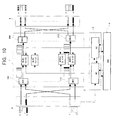
- FIG. 10 is an example arrangement for a common buffering device included in an ATM switching system.
- a cell buffering module 1 is connected to a highway line side via highway interfaces 5 and 6.
- a centrally located cell buffer memory consists of 16 buffer memories MEM0 to MEM15, and multiplexers (MUX) 100 to 115 and demultiplexers (DMUX) 200 to 215, which are included in a number equivalent to the buffer memory count.
- MUX multiplexers
- DMUX demultiplexers
- a write controller 2 and a read controller 3 are included as common buffer controllers, and an address buffer memory 4 is provided in association with the write controller 2 and the read controller 3.
- Each cell in the cell buffer memory has a capacity of 128K, and holds ATM cells stored in a bit slice form. Further, each bit of the 16 parallel bit sets constituting the ATM cell corresponds to one of the 16 buffer memories MEM0 to MEM15 which form the cell buffer memory.
- the ATM cell transmitted across each highway line for the highway interface 5 is divided into 16 bit slices each of which has a 32 bit width.
- the bit slices having the 32 bit widths are transmitted in parallel to the cell buffer module 1.
- the multiplexers MUX In the cell buffer module 1, identically numbered bits of the bit slices received in parallel are multiplexed by the multiplexers MUX. That is, in Fig. 10 , for example, of the 16 bit slices the multiplexer (MUX) 100 multiplexes the 1st bit which corresponds to the first bit of an ATM cell, and the multiplexer (MUX) 115 multiplexes the 16th bit slice.
- the bit slices multiplexed by the multiplexers (MUX) 100 to 115 are stored in parallel in the 16 buffer memories MEM0 to MEM15 for corresponding bits.
- the storage address is set by the write controller 2 of the common buffer controller.
- the storage address set by the write controller 2 is stored in the address buffer memory 4.
- the read controller 3 of the common buffer controller provides, as a read address, an address which corresponds to a write address, and 16 bit slices having a 32 bit width are read in parallel from the read address.
- the 16 bit slices read in parallel are separated by the demultiplexers (DMUX) 200 to 215, and are transmitted via the highway interface 6 to the destination lines.
- DMUX demultiplexers
- Fig. 11 is a diagram for explaining the procedures performed by the write controller 2 for setting and releasing the storage addresses.
- the ATM cells from the multiplexers (MUX) 100 to 115 are input (step S0) and TAG information for the cells is analyzed by the write controller 2, and an empty address ⁇ is defined as a write address a (step S1) and is written in the address buffer memory 4.
- the cell data are written at the write address ⁇ , which is set in the memories MEM0 to MEM15 in the cell buffer module 1 (step S2).
- the write controller 2 transmits as a read address the write address to the read control circuits RC1 to RCn, of the read controller 3, which correspond to the highway lines along which cell data to be read from the TAG information for the cell 100 is written to the address ⁇ (step S3).
- the read control circuits RC1 to RCn of the read controller 3 sequentially write received read addresses in the FIFO memory.
- the read control circuits RC1 to RCn then access read addresses ⁇ set by corresponding lines in the order in which they are written, and read the cell data therefrom (step S4).
- the read control circuits RC1 to RCn further notify the write controller 2 of the read address ⁇ at which cell data has been read (step S5).
- the write controller 2 Upon receipt of the read address ⁇ , the write controller 2 deletes and releases a corresponding write address ⁇ from the address buffer memory 4 (step S6).
- the write address of the cell buffer module 1 is released when the ATM cell is read from the buffer memories MEM0 to MEM15 by the read controller 3 and is transmitted to the highway line.
- the released address is stored as a write address for the ATM cell which will arrive next.
- the write address of the buffer module 1 is released and is stored as a write address for the ATM cell which will arrive next.
- a problem will arise when the received ATM cell is a multi-address call for transmitting the same cell to a plurality of lines.
- the cell buffer module 1 in Fig. 10 has a capacity of 128K. Accordingly, the address buffer memory 4 has a large capacity. Therefore, while taking into account how the common buffer device which uses an LSI is formed, providing such a large memory in the LSI is not advantageous.
- EP 0707397 provides a shared buffer memory switch for an ATM switching system and a broadcasting control method which can guarantee the cell transfer quality defined for each connection by maintaining the sequence order of arrival for each cell even if ordinary and broadcasting cells are mixed.
- bit map data showing a broadcasting destination information is read from a broadcast registration table based on the routing information derived from a header information of the cell, and an address for storing the cell in the shared buffer memory is written in all the address pointer queues of FIFOs corresponding to all output ports shown in the broadcasting destination information and the cell is stored in the shared buffer memory with the broadcasting destination information.
- an address of the shared buffer memory from which the cell is to be read out is read from the address pointer queue of FIFO, and the cell is output to the corresponding output port.
- the broadcasting destination information attached to the cell is reset for the corresponding output port and the revised broadcasting destination information and the cell is stored in the same address of the shared buffer memory until all broadcasting destination information are reset.
- a method for releasing an address in a common buffering device includes the steps of:
- a write table in a write table are entered a plurality of multi-address lines across which an ATM cell written at a specific address in the common buffering device can be multicast.
- a designation line for transmission of an ATM cell in a read control table is compared with the plurality of multi-address lines set in the write control table. When the lines match, the write address for the ATM cell, which is set in the write control table, is released.
- a line to which the ATM cell has been transmitted is added to the read control table.
- a write table in a write table are entered a plurality of multi-address lines across which is multicast an ATM cell written at a specific address in the common buffering device.
- a check is performed in advance to determine whether the same read addresses are present that have occurred during the period of time allocated for one cell, and bit sets are generated in the read control table.
- bit sets are generated in the read control table.
- Each time the ATM cell is read from the specific address, a corresponding bit set in the read control table is compared with the plurality of multi-address lines set in the write control table. When the bit set and the lines match, the write address which is set in the write control table for the ATM cell is released.
- the bit set is acquired by sequentially determining whether a read address for each adjacent read line is matched.
- the basic structure of a common buffering device which employs the above described address release method, comprises:
- the write controller compares the multi-address lines in the write control table with the line which is set in the read control table and to which the ATM cell is to be transmitted. When the lines match, the write address set by the write controller is released.
- the common buffer memory, the write control table and the read control table are constituted by an external memory.
- the write controller comprises:
- Fig. 1 is a block diagram illustrating the arrangement for carrying out the address release method for a common buffering device according to one embodiment of the present invention. An explanation will be given for the common buffering device shown in Fig. 1 , especially for the address release processing performed by the common buffer controller, which includes the write controller 2 and the read controller 3, features of the present invention.
- a feature of the present invention is that in the arrangement are provided a write control table 20 and a read control table 21.
- the write control table 20 and the read control table 21 can be stored as external memories in an address buffer memory 4 (see Fig. 10 ).
- the write controller 2 reads the TAG information in the ATM cell (step S00) and determines whether the ATM cell is a multi-address communication call. If the ATM cell is a multi-address communication call, destination lines are confirmed.
- Example TAG information included in an ATM cell is shown in Fig. 2 .
- a multi-address call instruction bit MC is set to 1.
- a destination highway line number is set to 1.
- highway lines 2 and 4 are set to 1, and the ATM cell is multicast to these lines.
- the write controller 2 searches for an empty address.
- An empty address ⁇ in the write control table (MCTW) 20 is set as a write address ⁇ (step S01).
- the write control table 20 includes N addresses, and a line, or lines, for which a channel should be set, i.e., a line to which the ATM cell should be multicast is set to "1" at the designated write address ⁇ .
- the lines 2 and 4 are set to 1.
- the write controller 2 accesses the designated address ⁇ in the buffer memories MEM0 to MEM15, which are prepared as external memories in this invention, so that a received ATM cell can be stored at the address ⁇ (step S02).
- the write controller 2 notifies one read control circuit, which corresponds to the destination line, that the address ⁇ is a read address ⁇ (step 03).
- the read control circuits (RC0 to RCn) 30 to 3n each include an FIFO memory, in which a read address received from the write controller 2 is sequentially stored. The addresses are read in the order in which they were stored, and the buffer memories MEM0 to MEM15 are accessed in order to read an ATM cell.
- the read control circuits (RC0 to RCn) 30 to 3n in accordance with the sizes of the queues of read addresses which are stored in the FIFO memories, have different timings at which to access the buffer memories MEM0 to MEM14.
- the read control circuits 30 to 3n upon receiving the read address ⁇ , the read control circuits 30 to 3n, in consonance with the different timings, read an ATM cell stored at the address ⁇ (step S04).
- the ATM cell data which are read are transmitted via a highway interface 6 (see Fig. 10 , not shown in Fig. 1 ).
- the read control circuits 30 to 3n return the address ⁇ , at which the ATM cell data were read, to the write controller 2 (step S05).
- the write controller 2 sets a "1" (sets a flag) for a line along which the multi-address cell was transmitted, at the read address ⁇ , which is included in the read control table 21 stored in the external memory and is returned by the read controller 3.
- the write controller 2 compares the line for which the write address ⁇ of the write control table 20 is registered with the contents of the line along which the multi-address ATM cell of the read control table 21 has been transmitted. When the contents match, the write address ⁇ is released (step S06).
- Fig. 3 is a detailed diagram showing the processing performed by the address release method for the common buffering device of this invention in order to provide a multi-address communication service for a plurality of lines.
- a detailed explanation is given for a comparison of the contents of the write control table 20 with those of the read control table 21.
- the address buffer module 1 has 4 x 4 switches, and accordingly, four lines, 1 to 4, are connected thereto. It is further assumed that of the lines 1 to 4 the ATM cell is multicast to lines 2 and 4.
- the pertinent write control circuit of the read controller 3 reads an ATM cell at the address ⁇ in the buffer memories MEM0 to MEM15, and notifies the write controller 2 that the ATM cell has been transmitted to line 4 (step S10).
- the write controller 2 Upon receiving this notification, the write controller 2 reads information for the lines (lines 2 and 4) for which the address ⁇ has been set by the write control table 20 and to which the ATM cell is multicast, and sets them in the register (step S11). At the same time, the write controller 2 reads information for the ATM cell destination lines, which are read from the address ⁇ recorded in the write control table 20 (step S12).
- step S10 since at step S10 the line 4 is the cell transmission line which is indicated when the read address ⁇ is returned, in the register a bit position which corresponds to the line 4 is set to "1" (step S13).
- step S15 Whether the registers match or not is determined by comparing them.
- step S16 the state of the register set at step S13 is recorded in the read control table 21 (step S16) and a notification that another multi-address line ATM cell has been read is waited for. The same processing as was previously performed is thereafter repeated.
- step S15 When at step S15 the states of the register match, i.e., when the ATM cell has been transmitted to all the multi-address destinations, the pertinent write address ⁇ in the write control table 20 and the associated multi-address destination information are cleared (step S17). Therefore, the write address ⁇ is freed and can be set as a write address for the next ATM cell that is received.
- the write control table 20 and the read control table 21 are constituted by an external memory, the relationship between the memory access time and the actual processing time must be taken, into consideration.
- the number of cells which are read during one cell time period is one for each highway line, and a maximum of four cells are read. Therefore, four read addresses are generated.
- the write controller 2 To determine whether an address should be released, the write controller 2 includes in a window one read process (step S12) and one write process (step S16). For the four addresses, four read processes and four write processes are included, and four windows are required.
- Fig. 4 is a time chart corresponding to the processing in Fig. 3 .
- the reference numerals for the steps in Fig. 4 correspond to those for the processing in Fig. 3 .
- it is assumed that the processing in Fig. 3 is performed upon the receipt from the read controller 3 of a notification (step S10') that an ATM cell has been multicast to line 2.
- step S16 At the time at which the information set in the write control table 20 is compared with the information stored in the read control table 21 (step S14'), the write operation to the read control table 21 for line 4 has not yet been performed (step S16).
- Fig. 5 is a flowchart for explaining the processing for the embodiment to resolve such a problem.
- Bit set generation step S1-1 is added to the processing in Fig. 3 .
- bit set generation process whether the same read addresses which are generated during a one cell time period are present is determined in advance for the generation of a bit set. Then, the processing as explained while referring to Fig. 3 is performed.
- the processing in Fig. 4 differs from that in Fig. 3 in that, when at read step S12 the read address ⁇ for line 4 is returned, a line which was read at the same address ⁇ during the previous reading process has already been determined by using a bit set.
- Figs. 6A and 6B copes with up to 8 x 8 switches.
- the write controller 2 compares the recently received read address with a read address which was received earlier.
- a highway line (HW) for an address which is transmitted to a comparison destination is shown relative to a corresponding highway line 0 to 7, which is an object of a bit set.
- highway line 0 is a highway used for comparison with the highway line 4 which is an object of a bit set
- highway lines 0 and 4 are those used for comparison with a highway line 1 which is an object of a bit set.
- a "1" is set to constitute a bit map.
- step S12 the data read from the read control table 21 indicate that an ATM cell has already been read from the read address ⁇ for line 2.
- step S13 for line 4 a "1" is set. The processing explained in Fig. 3 is thereafter performed.
- a bit map is generated in advance during a one cell time period. Then, before the processing in Fig. 5 is performed, at step S12 a bit position which represents the same address as a local address ⁇ , which was read and which corresponds to a line along which data was read earlier than the local reading time, and a bit position which corresponds to the local line are set to "1."
- Fig. 7 is shown the arrangement of the multi-address call processor which is included in the read controller 3 and which performs the processing in Fig. 6 .
- a bit set generator 300 includes flip-flops FF20 to 28 and address comparators 310 to 316. This example employs 8 x 8 switches, and the states of the multi-address destinations for highway lines (HW) 0 to 8 are set so as to correspond to the states of the flip-flops FF20 to 27, and are transmitted to the address comparators 310 to 316.
- HW highway lines
- the address comparators 310 to 316 compare the output of the flip-flop FF 20 with that of the respective flip-flops FF 21 to FF 27 at the following stages.
- bit set generator 300 is transmitted to a bit set circuit 301, which is a register, and is paired with the output of the flip-flop FF1. This processing corresponds to steps S12 and S13 in Fig. 5 .
- the comparator 302 which is constituted by three comparators COMP1 to COMP3 and the flip-flops FF6 to FF8, compares the output of the write control table 20 with the output of the bit set circuit 301, which is received via the flip-flop FF5. This process corresponds to step S14 in Fig. 5 .
- Figs. 9A and 9B are time charts for the arrangements in Figs. 7 and 8 .
- a read address a is latched by the write controller 2 at a latch clock (see c).
- bit set data are generated by the bit set generator 300 in Fig. 7 or 8 (see d).
- the address (see e) from the read controller 3 is updated and is written after 8 ⁇ has elapsed.
- the read address a is set by the read controller 3 (see g), a bit set is set (see h), and the two are compared.
- the comparison result is obtained after 3 ⁇ has elapsed (see i).
- the address release flag is output (see j).
- re-write data are fed back to the flip-flops F1 to FF4 in Fig. 6 .
- the common buffer memory can be provided as an external memory, and a design for the memory which uses an LSI can be facilitated. Furthermore, since the memory access time can be freely designated, the flexibility of the circuit can be improved.
Landscapes
- Engineering & Computer Science (AREA)
- Computer Networks & Wireless Communication (AREA)
- Signal Processing (AREA)
- Data Exchanges In Wide-Area Networks (AREA)
Claims (5)
- Procédé pour libérer une adresse dans un dispositif de tamponnage commun (1), lequel procédé inclut les étapes de :établissement d'une adresse d'écriture (α) dans ledit dispositif de tamponnage commun pour une cellule ATM qui doit être transmise sur une ou plusieurs lignes de destination prédéterminées ;écriture de la cellule ATM à l'adresse d'écriture (α) dans le dispositif de tamponnage commun ;lecture de la cellule ATM à partir de ladite adresse d'écriture (α) dans le dispositif de tamponnage commun (1) ;transmission de la cellule ATM lue sur les une ou plusieurs lignes de destination prédéterminées ; etlibération de l'adresse d'écriture (α),ledit procédé étant caractérisé en ce qu'il inclut en outre les étapes de :lecture de l'information dans la cellule ATM afin de confirmer les lignes de destination de ladite cellule ATM ;lorsque la cellule ATM doit être multidiffusée sur une pluralité de lignes de destination, établissement d'une pluralité de lignes à une adresse désignée dans une table de commande d'écriture (20) conformément à ladite information lue dans la cellule ATM ;chaque fois que la cellule ATM est lue à partir de l'adresse d'écriture (α) dans le dispositif de tamponnage commun (1), établissement d'un bit correspondant à la ligne de destination sur laquelle la cellule ATM a été transmise selon un jeu de bits d'une table de commande de lecture (21) et comparaison de chaque bit du jeu de bits dans la table de commande de lecture avec les lignes correspondantes établies au niveau de ladite adresse désignée dans la table de commande d'écriture (20) ; etlibération de l'adresse d'écriture (α) dans ledit dispositif de tamponnage commun lorsque toutes les lignes établies à ladite adresse désignée dans la table de commande d'écriture (20) correspondent à tous les bits établis dans le jeu de bits de la table de commande de lecture (21).
- Procédé de libération d'adresse selon la revendication 1, dans lequel ledit jeu de bits de ladite table de commande de lecture (21) est acquis en déterminant de façon séquentielle si oui ou non une adresse de lecture pour chaque ligne de lecture adjacente est en correspondance.
- Dispositif de tamponnage commun comprenant :une mémoire tampon commune (1) agencée pour stocker des cellules ATM ;un contrôleur d'écriture (2) adapté pour lire une information dans une cellule ATM afin de confirmer les lignes de destination de la cellule ATM et afin d'établir une adresse d'écriture (α) dans ladite mémoire tampon commune (1), adresse sur laquelle ladite cellule ATM est écrite et depuis laquelle elle est transmise sur les lignes de destination confirmées ;un contrôleur de lecture (30) adapté pour lire ladite cellule ATM à partir de ladite adresse d'écriture (α) dans la mémoire tampon commune (1) et pour transmettre ladite cellule ATM sur les lignes de destination confirmées ;une table de commande d'écriture 20 ; etune table de commande de lecture (21),dans lequel ledit dispositif est caractérisé en ce que :le dispositif de tamponnage commun est adapté pour établir dans une table de commande d'écriture (20) une pluralité de lignes correspondant aux lignes de destination sur lesquelles la cellule ATM écrite dans ladite mémoire tampon commune (1) doit être multidiffusée conformément à ladite information lue dans la cellule ATM ; etle dispositif de tamponnage commun est en outre adapté pour établir, dans une table de commande de lecture (21) comprenant un jeu de bits, chaque fois que ladite cellule ATM est envoyée sur chacune de ladite pluralité de lignes de destination établies au niveau de ladite adresse désignée de la table de commande d'écriture (20), un bit correspondant aux lignes de destination sur lesquelles ladite cellule ATM a été envoyée ; etledit contrôleur d'écriture (2) est en outre adapté pour libérer l'adresse d'écriture (α) dans ladite mémoire tampon commune (1) lorsque chacune de la pluralité de lignes établies à l'adresse désignée de la table de commande d'écriture (20) correspond auxdits bits correspondants dans le jeu de bits de la table de commande de lecture (21).
- Dispositif de tamponnage commun selon la revendication 3, dans lequel ladite mémoire tampon commune (1), ladite table de commande d'écriture (20) et ladite table de commande de lecture (21) sont constituées par une mémoire externe.
- Dispositif de tamponnage commun selon la revendication 3, dans lequel ledit contrôleur d'écriture (2) comprend :un registre (501) dans lequel des données établies séquentiellement indiquent la ligne de destination pour la transmission de ladite cellule ATM qui est lue par ledit contrôleur de lecture (30) ;un générateur de carte de bits ou bitmap adapté pour, chaque fois qu'une adresse de lecture d'une cellule ATM est retournée depuis le contrôleur de lecture et présente la même adresse dans ladite mémoire tampon commune qu'une adresse de lecture retournée plus tôt depuis le contrôleur de lecture, générer une carte de bits ou bitmap qui désigne la ligne de destination sur laquelle la cellule ATM a été transmise par le contrôleur de lecture ;un comparateur agencé pour réaliser une comparaison de ladite carte de bits ou bitmap générée par ledit générateur de bitmap avec une ligne correspondante dans ladite table de commande d'écriture, pour laquelle la même adresse d'écriture a été établie ; etun contrôleur adapté pour, suite à la réception du résultat de ladite comparaison, appliquer en retour sur ledit registre lesdites données indiquant quelle ligne de destination de transmission a été lue pour ladite cellule ATM ou pour mettre à zéro le contenu de ladite table de commande d'écriture.
Applications Claiming Priority (2)
| Application Number | Priority Date | Filing Date | Title |
|---|---|---|---|
| JP16689198 | 1998-06-15 | ||
| JP16689198A JP3604282B2 (ja) | 1998-06-15 | 1998-06-15 | アドレス開放方法及び、これを用いるatm交換システムの共通バッファ装置 |
Publications (3)
| Publication Number | Publication Date |
|---|---|
| EP0966174A2 EP0966174A2 (fr) | 1999-12-22 |
| EP0966174A3 EP0966174A3 (fr) | 2004-07-14 |
| EP0966174B1 true EP0966174B1 (fr) | 2008-04-09 |
Family
ID=15839551
Family Applications (1)
| Application Number | Title | Priority Date | Filing Date |
|---|---|---|---|
| EP19990101674 Expired - Lifetime EP0966174B1 (fr) | 1998-06-15 | 1999-02-05 | Méthode de libération d' addresses et dispositif de mémoire tampon partagée pour un système de commutation utilisant cette méthode |
Country Status (4)
| Country | Link |
|---|---|
| US (1) | US6789176B2 (fr) |
| EP (1) | EP0966174B1 (fr) |
| JP (1) | JP3604282B2 (fr) |
| DE (1) | DE69938478T2 (fr) |
Families Citing this family (6)
| Publication number | Priority date | Publication date | Assignee | Title |
|---|---|---|---|---|
| JP3604282B2 (ja) * | 1998-06-15 | 2004-12-22 | 富士通株式会社 | アドレス開放方法及び、これを用いるatm交換システムの共通バッファ装置 |
| US6822958B1 (en) * | 2000-09-25 | 2004-11-23 | Integrated Device Technology, Inc. | Implementation of multicast in an ATM switch |
| KR100358178B1 (ko) * | 2000-12-27 | 2002-10-25 | 한국전자통신연구원 | 공유메모리 스위치에서의 멀티캐스팅 장치 및 그 방법 |
| US7110405B2 (en) * | 2001-09-18 | 2006-09-19 | Integrated Device Technology, Inc. | Multicast cell buffer for network switch |
| US8225389B2 (en) * | 2003-04-11 | 2012-07-17 | Broadcom Corporation | Method and system to provide physical port security in a digital communication system |
| JP4832278B2 (ja) * | 2006-12-26 | 2011-12-07 | 富士通株式会社 | フレーム転送方法及び装置 |
Family Cites Families (17)
| Publication number | Priority date | Publication date | Assignee | Title |
|---|---|---|---|---|
| US5365519A (en) * | 1991-03-05 | 1994-11-15 | Hitachi, Ltd. | ATM switch1ng system connectable to I/O links having different transmission rates |
| JP2549200B2 (ja) | 1990-08-31 | 1996-10-30 | 三菱電機株式会社 | セル交換装置 |
| DE69433229T2 (de) * | 1993-02-15 | 2004-08-12 | Mitsubishi Denki K.K. | ATM-Schalter |
| US5537400A (en) * | 1994-04-15 | 1996-07-16 | Dsc Communications Corporation | Buffered crosspoint matrix for an asynchronous transfer mode switch and method of operation |
| DE69428186T2 (de) * | 1994-04-28 | 2002-03-28 | Hewlett-Packard Co.(A Delaware Corporation), Palo Alto | Mehrfachsendeeinrichtung |
| JPH07321815A (ja) * | 1994-05-24 | 1995-12-08 | Nec Corp | 共有バッファ型atmスイッチおよびその同報制御方法 |
| US5528588A (en) * | 1994-09-14 | 1996-06-18 | Fore Systems, Inc. | Multicast shared memory |
| GB2303274B (en) * | 1995-07-11 | 1999-09-08 | Fujitsu Ltd | Switching apparatus |
| JPH0991172A (ja) | 1995-09-20 | 1997-04-04 | Fujitsu Ltd | メモリ制御状態監視装置 |
| JP2842522B2 (ja) * | 1995-12-06 | 1999-01-06 | 日本電気株式会社 | Atmスイッチ及びその制御方法 |
| KR100387048B1 (ko) * | 1996-03-30 | 2003-08-21 | 삼성전자주식회사 | 중저속 가입자 멀티 캐스팅 구현 방법 및 장치 |
| JP3473262B2 (ja) * | 1996-04-05 | 2003-12-02 | 株式会社日立製作所 | パケット通信装置 |
| US5898687A (en) * | 1996-07-24 | 1999-04-27 | Cisco Systems, Inc. | Arbitration mechanism for a multicast logic engine of a switching fabric circuit |
| US6101187A (en) * | 1996-12-20 | 2000-08-08 | International Business Machines Corporation | Method and system for multicasting cells in an ATM protocol adapter |
| US6385198B1 (en) * | 1998-06-11 | 2002-05-07 | Synchrodyne Networks, Inc. | Signaling for timely forwarding in packet switching network with a common time reference |
| JP3604282B2 (ja) * | 1998-06-15 | 2004-12-22 | 富士通株式会社 | アドレス開放方法及び、これを用いるatm交換システムの共通バッファ装置 |
| JP4489308B2 (ja) * | 2001-01-05 | 2010-06-23 | 富士通株式会社 | パケットスイッチ |
-
1998
- 1998-06-15 JP JP16689198A patent/JP3604282B2/ja not_active Expired - Fee Related
-
1999
- 1999-02-05 EP EP19990101674 patent/EP0966174B1/fr not_active Expired - Lifetime
- 1999-02-05 DE DE1999638478 patent/DE69938478T2/de not_active Expired - Fee Related
- 1999-04-05 US US09/286,332 patent/US6789176B2/en not_active Expired - Fee Related
Also Published As
| Publication number | Publication date |
|---|---|
| EP0966174A3 (fr) | 2004-07-14 |
| JP3604282B2 (ja) | 2004-12-22 |
| US6789176B2 (en) | 2004-09-07 |
| DE69938478D1 (de) | 2008-05-21 |
| US20020145995A1 (en) | 2002-10-10 |
| JP2000004233A (ja) | 2000-01-07 |
| EP0966174A2 (fr) | 1999-12-22 |
| DE69938478T2 (de) | 2009-05-07 |
Similar Documents
| Publication | Publication Date | Title |
|---|---|---|
| US5825767A (en) | ATM switch with input and output ports | |
| CA2149973C (fr) | Commutateur de memoire tampon commune pour systeme de commutation mta et methode de controle de diffusion connexe | |
| JP2788577B2 (ja) | フレーム変換方法及び装置 | |
| US5893162A (en) | Method and apparatus for allocation and management of shared memory with data in memory stored as multiple linked lists | |
| US4849968A (en) | Buffer management system | |
| EP0118446B1 (fr) | Configuration de memoire a systeme premier entre, premier sorti (fifo) pour un stockage en file d'attente | |
| EP0379709B1 (fr) | Commutateur de combinaison à grande vitesse utilisant un seul tampon PEPS | |
| US3979733A (en) | Digital data communications system packet switch | |
| US20020116535A1 (en) | Method and apparatus for managing the flow of data within a switching device | |
| EP0545575A1 (fr) | Dispositif de mémoires FIFO virtuelles multiples | |
| JP2865692B2 (ja) | スイッチングシステム及びその構成方法 | |
| US6728256B1 (en) | Shared buffer control device | |
| EP1030483A1 (fr) | Commutateur ATM | |
| US5926475A (en) | Method and apparatus for ensuring ATM cell order in multiple cell transmission lane switching system | |
| EP0966174B1 (fr) | Méthode de libération d' addresses et dispositif de mémoire tampon partagée pour un système de commutation utilisant cette méthode | |
| JP2628701B2 (ja) | 優先順位付き情報パケット用交換装置 | |
| JP3207867B2 (ja) | 同様の装置を管理する方法および回路装置およびスイッチ素子 | |
| KR100279949B1 (ko) | 셀 재배열 버퍼 | |
| US7075938B1 (en) | Common buffer memory control apparatus | |
| EP0454797B1 (fr) | Systeme de commutation a multiplexage temporel asynchrone | |
| JP3103298B2 (ja) | Atmスイッチのアドレス生成回路 | |
| US4251684A (en) | Data storage systems | |
| Choudhury et al. | New implementation of multi-priority pushout for shared memory ATM switches | |
| JP3169510B2 (ja) | データ待ち行列装置 | |
| JPH0833869B2 (ja) | データ処理装置 |
Legal Events
| Date | Code | Title | Description |
|---|---|---|---|
| PUAI | Public reference made under article 153(3) epc to a published international application that has entered the european phase |
Free format text: ORIGINAL CODE: 0009012 |
|
| AK | Designated contracting states |
Kind code of ref document: A2 Designated state(s): AT BE CH CY DE DK ES FI FR GB GR IE IT LI LU MC NL PT SE |
|
| AX | Request for extension of the european patent |
Free format text: AL;LT;LV;MK;RO;SI |
|
| PUAL | Search report despatched |
Free format text: ORIGINAL CODE: 0009013 |
|
| AK | Designated contracting states |
Kind code of ref document: A3 Designated state(s): AT BE CH CY DE DK ES FI FR GB GR IE IT LI LU MC NL PT SE |
|
| AX | Request for extension of the european patent |
Extension state: AL LT LV MK RO SI |
|
| 17P | Request for examination filed |
Effective date: 20050105 |
|
| 17Q | First examination report despatched |
Effective date: 20050202 |
|
| AKX | Designation fees paid |
Designated state(s): DE FR GB |
|
| 17Q | First examination report despatched |
Effective date: 20050202 |
|
| GRAP | Despatch of communication of intention to grant a patent |
Free format text: ORIGINAL CODE: EPIDOSNIGR1 |
|
| GRAS | Grant fee paid |
Free format text: ORIGINAL CODE: EPIDOSNIGR3 |
|
| GRAA | (expected) grant |
Free format text: ORIGINAL CODE: 0009210 |
|
| AK | Designated contracting states |
Kind code of ref document: B1 Designated state(s): DE FR GB |
|
| REG | Reference to a national code |
Ref country code: GB Ref legal event code: FG4D |
|
| REF | Corresponds to: |
Ref document number: 69938478 Country of ref document: DE Date of ref document: 20080521 Kind code of ref document: P |
|
| ET | Fr: translation filed | ||
| PLBE | No opposition filed within time limit |
Free format text: ORIGINAL CODE: 0009261 |
|
| STAA | Information on the status of an ep patent application or granted ep patent |
Free format text: STATUS: NO OPPOSITION FILED WITHIN TIME LIMIT |
|
| 26N | No opposition filed |
Effective date: 20090112 |
|
| PGFP | Annual fee paid to national office [announced via postgrant information from national office to epo] |
Ref country code: DE Payment date: 20090225 Year of fee payment: 11 |
|
| PGFP | Annual fee paid to national office [announced via postgrant information from national office to epo] |
Ref country code: GB Payment date: 20090129 Year of fee payment: 11 |
|
| PGFP | Annual fee paid to national office [announced via postgrant information from national office to epo] |
Ref country code: FR Payment date: 20090114 Year of fee payment: 11 |
|
| GBPC | Gb: european patent ceased through non-payment of renewal fee |
Effective date: 20100205 |
|
| REG | Reference to a national code |
Ref country code: FR Ref legal event code: ST Effective date: 20101029 |
|
| PG25 | Lapsed in a contracting state [announced via postgrant information from national office to epo] |
Ref country code: FR Free format text: LAPSE BECAUSE OF NON-PAYMENT OF DUE FEES Effective date: 20100301 |
|
| PG25 | Lapsed in a contracting state [announced via postgrant information from national office to epo] |
Ref country code: DE Free format text: LAPSE BECAUSE OF NON-PAYMENT OF DUE FEES Effective date: 20100901 |
|
| PG25 | Lapsed in a contracting state [announced via postgrant information from national office to epo] |
Ref country code: GB Free format text: LAPSE BECAUSE OF NON-PAYMENT OF DUE FEES Effective date: 20100205 |