EP0967562A2 - Méthode de communication pour carte d'identification et circuit intégré utilisé dans ladite carte - Google Patents
Méthode de communication pour carte d'identification et circuit intégré utilisé dans ladite carte Download PDFInfo
- Publication number
- EP0967562A2 EP0967562A2 EP99110563A EP99110563A EP0967562A2 EP 0967562 A2 EP0967562 A2 EP 0967562A2 EP 99110563 A EP99110563 A EP 99110563A EP 99110563 A EP99110563 A EP 99110563A EP 0967562 A2 EP0967562 A2 EP 0967562A2
- Authority
- EP
- European Patent Office
- Prior art keywords
- waveform
- circuit
- terminal
- output
- master
- Prior art date
- Legal status (The legal status is an assumption and is not a legal conclusion. Google has not performed a legal analysis and makes no representation as to the accuracy of the status listed.)
- Granted
Links
Images





Classifications
-
- G—PHYSICS
- G06—COMPUTING OR CALCULATING; COUNTING
- G06K—GRAPHICAL DATA READING; PRESENTATION OF DATA; RECORD CARRIERS; HANDLING RECORD CARRIERS
- G06K7/00—Methods or arrangements for sensing record carriers, e.g. for reading patterns
- G06K7/0008—General problems related to the reading of electronic memory record carriers, independent of its reading method, e.g. power transfer
-
- H—ELECTRICITY
- H04—ELECTRIC COMMUNICATION TECHNIQUE
- H04L—TRANSMISSION OF DIGITAL INFORMATION, e.g. TELEGRAPHIC COMMUNICATION
- H04L25/00—Baseband systems
- H04L25/38—Synchronous or start-stop systems, e.g. for Baudot code
- H04L25/40—Transmitting circuits; Receiving circuits
- H04L25/49—Transmitting circuits; Receiving circuits using code conversion at the transmitter; using predistortion; using insertion of idle bits for obtaining a desired frequency spectrum; using three or more amplitude levels ; Baseband coding techniques specific to data transmission systems
- H04L25/4904—Transmitting circuits; Receiving circuits using code conversion at the transmitter; using predistortion; using insertion of idle bits for obtaining a desired frequency spectrum; using three or more amplitude levels ; Baseband coding techniques specific to data transmission systems using self-synchronising codes, e.g. split-phase codes
Definitions
- the present invention is related to a communication method of a contactless ID card and also to a circuit for realizing this communication method, and is to provide a communication method with employment of a code capable of readily separating data from a clock, and to provide a circuit for realizing this communication method, and further, to provide a transmitter, a receiver utilized in this communication method, and a communication system.
- the contactless ID cards are classified into a close coupling type ID card used, while being coupled to a sensor; a proximity type ID card used, while being separated from a sensor by approximately 20 cm; and a remote type ID card used, while being separated from a sensor by approximately 50 cm.
- the close coupling type ID cards are mainly applied to credit cards.
- the proximity type ID cards are applied to commuter passes and ID cards.
- the remote type ID cards are applied to TAGs of logistic systems.
- the close coupling type ID cards and the proximity type ID cards receive supplies of information and electric power by way of mainly magnetic fields.
- the remote type ID cards receive supplies of these information and electric power by way of electromagnetic waves.
- the remote type ID cards own the following development problems since the received electric power is very weak. That is, more specifically, the remote type ID cards are operable under low power consumption, and also the electric power is supplied in high efficiencies.
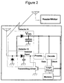
- Fig. 2 shows an example of a remote type contactless ID card system.
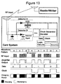
- An IC card is arranged by an antenna, a diode for detection, a diode for a power supply voltage generator, a preamplifier, a clock generator, a decoding circuit, a logic control circuit, a memory, a driving FET for answering, and so on.
- An amplitude modulation signal containing information of a clock and data is transmitted from a reader/writer.
- a signal When a signal is received, electric charges are stored into a power capacitor, and then the IC card is operated by using a voltage appearing across the capacitor as a power supply voltage.
- the signal detected by a detector is separated into the data and the clock by the clock generator and the decoding circuit, which are processed by the logic control circuit.
- an impedance of the antenna is modulated by the driving FET for answering.
- the Manchester code is applied so as to communicate the data between the ID cards and the data readers/writers, as described in "A Low-Power CMOS Integrated Circuit for Field-Powered Radio Frequency Identification Tags", by D. Friendman et.al., IEEE ISSCC97, SA.17.5, 1997.
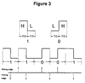
- Fig. 3 indicates a modulation waveform by the Manchester code.
- a transition from "H (high voltage)” state to "L (low voltage)” state is allocated to 1
- a transition from "L (low voltage)” state to "H (high voltage)” state is allocated to 0.
- time of "H” is not equal to time of "L", namely a duty ratio is not equal to 50%
- a DC offset is produced by data.
- a level of a received signal is varied, or fluctuated, this fluctuation mainly causes reading errors.
- the time of "H” is set to be equal to the time of "L” so as to realize the signal having the duty ratio of 50%, and the code suitable for the communication is realized without the occurrence of the DC offset.
- the locking condition of the phase-locked loop is given by that the self-running frequency of the oscillator is defined within +50% and -50% of the frequency of the reference signal. To satisfy this condition, the temperature, the power supply voltage, and the process fluctuation of the device must be canceled, and a complex reference circuit is required, and thus, the consumed current is increased. In such a case that the communication is temporarily interrupted due to adverse influences caused by electromagnetic wave conditions, there is such a problem that the convergence of clocks is prolonged, and thus, lengthy locking time is required.
- An object of the present invention is to provide a communication method, a circuit capable of realizing this communication method, and also to provide a transmitter, a receiver, and a communication system, which are used in this communication method, to reproduce a code without employing a complex phase-locked loop, to produce a reference clock of an integrated circuit provided on a card, and also capable of satisfying a duty ratio of 50%, and further, to provide a demodulating circuit for demodulating this code.
- An object of the present invention is to provide a system.
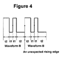
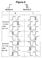
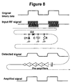
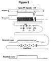
- a plurality of waveform patterns each having a duty ratio of 50% are combined with such a waveform maintained in order not produce the same transition (rising edge, or falling edge) as that of a center of the waveform at a joint portion of the waveform, and by allocating "1" and "0". Either a rising edge or a falling edge appears at a near center of the waveform pattern.
- Fig. 13 represents a card system and operation timing thereof.
- the waveform patterns of this present invention own various selection possibilities.
- such a pattern that rising-edge transitions appear in an equi-interval is employed.
- a modulation system employed therein is the ASK (Amplitude-shift Keying) system such that the carrier signal is transmitted under High state, and the carrier is stopped under Low state.
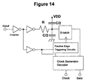
- FIG. 14 A sixth embodiment mode of the present invention will now be explained with reference to Fig. 14.
- This embodiment may reduce an adverse influence given to a decoder when a power supply voltage is varied.
- the card system without having the cell detects the signal and smoothes the detected signal so as to obtain the power supply voltage.
- the power supply voltage is readily varied, depending upon operation conditions of the circuit.
- the logic threshold value of the inverter circuit for driving the LPF, and the logic threshold value of the D-latch circuit for sampling the signal are varied due to the voltage variation.
- the capacitance of the LPF is subdivided into two capacitances which are then connected to both the ground terminal and the power supply terminal.
- both the clock and the data can be simultaneously transmitted, and can be readily decoded without using such a complex PLL circuit.
- the decoding circuit with less erroneous operation with respect to the variations contained in the power supply voltage is realized.
- test chip was trial-manufactured by way of the 0.8 ⁇ m CMOS standard process.
- the trial-manufactured chip contains all of the circuits except for the memory and the diode for detection.
- the RC filter provided in the demodulating circuit was also manufactured as the integrated circuit.
- the evaluation result about the entire test chip is listed in a table 1.
- Vth variation +0.1V and -0.1V by process variations, within a temperature range between -10 deg. C and 90 deg. C, and within a power supply voltage range from 1.8 V to 7 V. That is, with respect to an input of 0.1 Vpp, the decoder was operated with the error rate less than 10 -6 . When the amplitude of the input signal was increased up to the power supply voltage level, the confirmation was made that the decoder could be operated even under -30 deg. C and 1.6 V power supply. The consumed current may depend upon the operating condition. The confirmation was made that the current from 15 ⁇ A to approximately 70 ⁇ A was consumed under such a condition the average current was 40 ⁇ A.
- the system operation was carried out by way of the test board on which the diode and ROM were mounted.
- the electric power of 1 mW at 2.45 GHz, which is equivalent to the communication distance of 1.5 m was supplied to the diode detecting circuit.
- the diode detecting circuit owns the current supply capability of approximately 100 ⁇ A. Under this condition, such a confirmation was made that the test board was that the test board was operated without employing any external power supply.
- the effects of the present invention could be proved by way of the above-described experiments.
Landscapes
- Engineering & Computer Science (AREA)
- Physics & Mathematics (AREA)
- Computer Vision & Pattern Recognition (AREA)
- Computer Networks & Wireless Communication (AREA)
- Signal Processing (AREA)
- Artificial Intelligence (AREA)
- Spectroscopy & Molecular Physics (AREA)
- General Physics & Mathematics (AREA)
- Theoretical Computer Science (AREA)
- Near-Field Transmission Systems (AREA)
- Digital Transmission Methods That Use Modulated Carrier Waves (AREA)
- Mobile Radio Communication Systems (AREA)
- Dc Digital Transmission (AREA)
- Small-Scale Networks (AREA)
- Semiconductor Integrated Circuits (AREA)
Applications Claiming Priority (2)
| Application Number | Priority Date | Filing Date | Title |
|---|---|---|---|
| JP15714498 | 1998-06-05 | ||
| JP15714498A JP3531477B2 (ja) | 1998-06-05 | 1998-06-05 | 非接触カードの通信方法及び該通信に用いる集積回路 |
Publications (3)
| Publication Number | Publication Date |
|---|---|
| EP0967562A2 true EP0967562A2 (fr) | 1999-12-29 |
| EP0967562A3 EP0967562A3 (fr) | 2003-05-07 |
| EP0967562B1 EP0967562B1 (fr) | 2004-12-15 |
Family
ID=15643152
Family Applications (1)
| Application Number | Title | Priority Date | Filing Date |
|---|---|---|---|
| EP99110563A Expired - Lifetime EP0967562B1 (fr) | 1998-06-05 | 1999-06-01 | Méthode de communication |
Country Status (4)
| Country | Link |
|---|---|
| US (2) | US6765959B1 (fr) |
| EP (1) | EP0967562B1 (fr) |
| JP (1) | JP3531477B2 (fr) |
| DE (1) | DE69922587T2 (fr) |
Cited By (3)
| Publication number | Priority date | Publication date | Assignee | Title |
|---|---|---|---|---|
| FR2877520A1 (fr) * | 2004-11-04 | 2006-05-05 | St Microelectronics Sa | Procede et dispositif de generation d'horloge de decodage a partir d'un signal asynchrone de donnees base sur la norme epc global |
| WO2008134133A1 (fr) * | 2007-04-27 | 2008-11-06 | Continental Automotive Systems Us, Inc. | Système de communication de signaux à distance présentant une meilleure performance de réception |
| CN1698330B (zh) * | 2003-01-15 | 2010-04-28 | 日本电信电话株式会社 | 非接触rf id系统的通信方法,非接触rf id系统,发报机以及接收机 |
Families Citing this family (19)
| Publication number | Priority date | Publication date | Assignee | Title |
|---|---|---|---|---|
| US7522878B2 (en) * | 1999-06-21 | 2009-04-21 | Access Business Group International Llc | Adaptive inductive power supply with communication |
| US7212414B2 (en) | 1999-06-21 | 2007-05-01 | Access Business Group International, Llc | Adaptive inductive power supply |
| FR2830700A1 (fr) * | 2001-10-09 | 2003-04-11 | Koninkl Philips Electronics Nv | Dispositif de generation d'un signal d'horloge |
| JP4145583B2 (ja) * | 2002-07-02 | 2008-09-03 | シャープ株式会社 | 信号伝送方法、信号伝送システム、論理回路、及び液晶駆動装置 |
| DE10244450A1 (de) * | 2002-09-24 | 2004-04-01 | Infineon Technologies Ag | Verfahren und Schaltungsanordnung zur Demodulation eines digitalen amplitudenmodulierten Funksignals |
| TWI230927B (en) * | 2003-10-08 | 2005-04-11 | Mediatek Inc | Sawtooth wobble bit value detector |
| DE102004016335B4 (de) * | 2004-04-02 | 2019-06-13 | Infineon Technologies Ag | Verfahren zur kontaktlosen Datenübertragung |
| US7058138B2 (en) * | 2004-09-01 | 2006-06-06 | Xg Technology, Llc | Coordinated numerical control of sideband energy and modulation compression method for the radio frequency transmission of high speed data |
| JP4836489B2 (ja) * | 2005-05-12 | 2011-12-14 | オンセミコンダクター・トレーディング・リミテッド | 駆動波発生回路 |
| US7821378B2 (en) * | 2005-09-29 | 2010-10-26 | Electronics And Telecommunications Research Institute | Apparatus and method for receiving tag signal in mobile RFID reader |
| JP2008269688A (ja) * | 2007-04-18 | 2008-11-06 | Toshiba Samsung Storage Technology Corp | 光ディスク及び光ディスク装置 |
| US8000652B2 (en) * | 2008-02-11 | 2011-08-16 | Sony Ericsson Mobile Communications Ab | Sending and receiving information |
| JP4596038B2 (ja) * | 2008-05-12 | 2010-12-08 | ソニー株式会社 | 送信装置および方法、受信装置および方法、並びにプログラム |
| JP5184278B2 (ja) * | 2008-09-22 | 2013-04-17 | 株式会社横須賀テレコムリサーチパーク | 波形生成回路およびタグ通信装置 |
| JP6390043B2 (ja) * | 2012-02-28 | 2018-09-19 | 株式会社国際電気通信基礎技術研究所 | 送信機、それにおける送信方法、送信機から無線信号を受信する受信機およびそれらを備える無線通信システム |
| US9423843B2 (en) * | 2012-09-21 | 2016-08-23 | Atmel Corporation | Processor maintaining reset-state after reset signal is suspended |
| JP6249401B2 (ja) * | 2013-05-30 | 2017-12-20 | 学校法人上智学院 | 通信装置及び通信システム |
| CN111226423A (zh) * | 2017-10-19 | 2020-06-02 | 瑞典爱立信有限公司 | 用于发送二进制信息的发射机、网络节点、方法及计算机程序 |
| US10958412B1 (en) | 2020-01-22 | 2021-03-23 | Infineon Technologies Ag | Communication using edge timing in a signal |
Family Cites Families (27)
| Publication number | Priority date | Publication date | Assignee | Title |
|---|---|---|---|---|
| JPS5623065A (en) * | 1980-05-15 | 1981-03-04 | Sanyo Electric Co Ltd | Demodulation circuit for self clocking information signal |
| NL8102593A (nl) * | 1981-05-27 | 1982-12-16 | Philips Nv | Fm-omroepstelsel met zenderkarakterisering door middel van een binair fasegemoduleerd, differentieel gecodeerd codesignaal. |
| US4471345A (en) * | 1982-03-05 | 1984-09-11 | Sensormatic Electronics Corporation | Randomized tag to portal communication system |
| JPS60171475A (ja) * | 1984-02-15 | 1985-09-04 | アイデンティフィケ−ション・デバイセス・インコ−ポレ−テッド | 識別システム |
| ATE108965T1 (de) * | 1987-12-09 | 1994-08-15 | Omron Tateisi Electronics Co | Induktives datenübertragungssystem. |
| US5127023A (en) * | 1990-07-18 | 1992-06-30 | The United States Of America As Represented By The Secretary Of The Navy | Retiming decoder/encoder |
| US5131014A (en) * | 1991-04-19 | 1992-07-14 | General Instrument Corporation | Apparatus and method for recovery of multiphase modulated data |
| US5754250A (en) * | 1992-02-18 | 1998-05-19 | Cooper; J. Carl | Synchronizing signal separating apparatus and method |
| NZ314270A (en) * | 1992-11-18 | 1998-06-26 | British Tech Group | Transponder identification system: interrogator transmits inhibiting signal to disable transponders |
| US5287330A (en) * | 1993-01-04 | 1994-02-15 | Westinghouse Electric Corp. | Sonar apparatus |
| DE4303356A1 (de) * | 1993-02-05 | 1994-08-11 | Philips Patentverwaltung | Digitale Phasenregelschleife |
| US5568516A (en) * | 1993-07-02 | 1996-10-22 | Phonic Ear Incorporated | Very low power cordless headset system |
| US6308554B1 (en) * | 1994-03-12 | 2001-10-30 | Robert Bosch Gmbh | Electronic device having an acceleration-sensitive sensor |
| JPH0877318A (ja) * | 1994-09-08 | 1996-03-22 | Toshiba Corp | 非接触式情報記録媒体 |
| US5636248A (en) * | 1994-10-04 | 1997-06-03 | The United States Of America As Represented By The Secretary Of The Navy | Method and system for regenerating amplitude and timing characteristics of an analog signal |
| US5661373A (en) * | 1995-03-13 | 1997-08-26 | Nishizawa; Atsushi | Binary digital signal transmission system using binary digital signal of electrically discharged pulse and method for transmitting binary digital signal |
| JPH08250686A (ja) | 1995-03-14 | 1996-09-27 | Kawasaki Steel Corp | 発振回路 |
| US5502711A (en) * | 1995-03-20 | 1996-03-26 | International Business Machines Corporation | Dual digital phase locked loop clock channel for optical recording |
| US5990939A (en) * | 1995-09-28 | 1999-11-23 | Raytheon Company | Video demultiplexing interface for a missile tracking system |
| KR970055245A (ko) * | 1995-12-30 | 1997-07-31 | 김광호 | 에프.엠 복조 회로 |
| US5780828A (en) * | 1996-02-15 | 1998-07-14 | Dh Technology, Inc. | Interactive video systems |
| JP4001955B2 (ja) | 1996-06-18 | 2007-10-31 | ソニー株式会社 | ディジタル信号の伝送方法 |
| JPH10163756A (ja) * | 1996-11-28 | 1998-06-19 | Fujitsu Ltd | 自動周波数制御装置 |
| US6038265A (en) * | 1997-04-21 | 2000-03-14 | Motorola, Inc. | Apparatus for amplifying a signal using digital pulse width modulators |
| US6148048A (en) * | 1997-09-26 | 2000-11-14 | Cirrus Logic, Inc. | Receive path implementation for an intermediate frequency transceiver |
| US5901054A (en) * | 1997-12-18 | 1999-05-04 | Chun-Shan Institute Of Science And Technology | Pulse-width-modulation control circuit |
| US6166606A (en) * | 1999-02-10 | 2000-12-26 | Zilog, Inc. | Phase and frequency locked clock generator |
-
1998
- 1998-06-05 JP JP15714498A patent/JP3531477B2/ja not_active Expired - Fee Related
-
1999
- 1999-06-01 EP EP99110563A patent/EP0967562B1/fr not_active Expired - Lifetime
- 1999-06-01 DE DE69922587T patent/DE69922587T2/de not_active Expired - Fee Related
- 1999-06-04 US US09/325,801 patent/US6765959B1/en not_active Expired - Fee Related
-
2004
- 2004-06-04 US US10/860,324 patent/US7116709B2/en not_active Expired - Fee Related
Cited By (7)
| Publication number | Priority date | Publication date | Assignee | Title |
|---|---|---|---|---|
| CN1698330B (zh) * | 2003-01-15 | 2010-04-28 | 日本电信电话株式会社 | 非接触rf id系统的通信方法,非接触rf id系统,发报机以及接收机 |
| US7738838B2 (en) | 2003-01-15 | 2010-06-15 | Nippon Telegraph And Telephone Corporation | Non-contact RF ID system communication method, non-contact RF ID system, transmitter, and receiver |
| EP1585280A4 (fr) * | 2003-01-15 | 2011-09-21 | Nippon Telegraph & Telephone | Procede de communication d'un systeme d'identification hf sans contact, systeme d'identification hf sans contact, emetteur et recepteur |
| FR2877520A1 (fr) * | 2004-11-04 | 2006-05-05 | St Microelectronics Sa | Procede et dispositif de generation d'horloge de decodage a partir d'un signal asynchrone de donnees base sur la norme epc global |
| EP1670200A1 (fr) * | 2004-11-04 | 2006-06-14 | Stmicroelectronics Sa | Procédé et dispositif de génération d'horloge de décodage à partir d'un signal asynchrone de données basé sur la norme EPC global |
| US7614564B2 (en) | 2004-11-04 | 2009-11-10 | Stmicroelectronics Sa | Clock generation method and device for decoding from an asynchronous data signal |
| WO2008134133A1 (fr) * | 2007-04-27 | 2008-11-06 | Continental Automotive Systems Us, Inc. | Système de communication de signaux à distance présentant une meilleure performance de réception |
Also Published As
| Publication number | Publication date |
|---|---|
| US6765959B1 (en) | 2004-07-20 |
| US7116709B2 (en) | 2006-10-03 |
| JP3531477B2 (ja) | 2004-05-31 |
| EP0967562B1 (fr) | 2004-12-15 |
| JPH11355365A (ja) | 1999-12-24 |
| EP0967562A3 (fr) | 2003-05-07 |
| US20040228400A1 (en) | 2004-11-18 |
| DE69922587D1 (de) | 2005-01-20 |
| DE69922587T2 (de) | 2005-12-08 |
Similar Documents
| Publication | Publication Date | Title |
|---|---|---|
| US6765959B1 (en) | Communication method of contactless ID card and integrated circuit used in communication method | |
| US5418353A (en) | Non-contact, electromagnetically coupled transmission and receiving system for IC cards | |
| EP0171433B1 (fr) | Systeme d'identificationet transpondeur | |
| US8218703B2 (en) | Methods of processing a wireless communication signal, wireless communication synchronization methods, and a radio frequency identification device communication method | |
| US5889273A (en) | Wireless communication data storing medium for receiving a plurality of carriers of proximate frequencies and a transmission/receiving method | |
| US5862174A (en) | Data storage medium | |
| USRE44415E1 (en) | Wireless communication medium and method for operating the same | |
| EP2486665B1 (fr) | Démodulateur hdx | |
| US5553099A (en) | FSK detector for determining an increasing time period between adjacent pulses of an FSK modulated square wave pulse train | |
| EP0525642B1 (fr) | Système de lecture/écriture pour moyen d'enregistrement et système de carte à puce de non-contact | |
| US20100245051A1 (en) | Communication Method for Noncontact RF ID System, Noncontact RF ID System, and Transmitter and Receiver | |
| JPH05236031A (ja) | データ伝送方式 | |
| US12423533B2 (en) | Reception circuit and smart card including the same | |
| US8253469B2 (en) | Semiconductor device | |
| US12244363B1 (en) | Tag with advanced clock extraction | |
| JP2005151033A (ja) | Rfid通信におけるvpm変調方式 | |
| JP2000059261A (ja) | 非接触データ送受信装置 | |
| Garade et al. | INTERNATIONAL JOURNAL OF ENGINEERING SCIENCES & RESEARCH TECHNOLOGY FULLY REUSED VLSI ARCHITECTURE OF DSRC ENCODERS USING SOLS |
Legal Events
| Date | Code | Title | Description |
|---|---|---|---|
| PUAI | Public reference made under article 153(3) epc to a published international application that has entered the european phase |
Free format text: ORIGINAL CODE: 0009012 |
|
| AK | Designated contracting states |
Kind code of ref document: A2 Designated state(s): AT BE CH CY DE DK ES FI FR GB GR IE IT LI LU MC NL PT SE |
|
| AX | Request for extension of the european patent |
Free format text: AL;LT;LV;MK;RO;SI |
|
| RIC1 | Information provided on ipc code assigned before grant |
Free format text: 7G 06K 7/00 A, 7H 04L 25/49 B, 7G 06K 19/07 B |
|
| PUAL | Search report despatched |
Free format text: ORIGINAL CODE: 0009013 |
|
| AK | Designated contracting states |
Designated state(s): AT BE CH CY DE DK ES FI FR GB GR IE IT LI LU MC NL PT SE |
|
| AX | Request for extension of the european patent |
Extension state: AL LT LV MK RO SI |
|
| 17P | Request for examination filed |
Effective date: 20031106 |
|
| AKX | Designation fees paid |
Designated state(s): DE FR GB |
|
| 17Q | First examination report despatched |
Effective date: 20031219 |
|
| GRAP | Despatch of communication of intention to grant a patent |
Free format text: ORIGINAL CODE: EPIDOSNIGR1 |
|
| RTI1 | Title (correction) |
Free format text: COMMUNICATION METHOD |
|
| RTI1 | Title (correction) |
Free format text: COMMUNICATION METHOD |
|
| GRAS | Grant fee paid |
Free format text: ORIGINAL CODE: EPIDOSNIGR3 |
|
| GRAA | (expected) grant |
Free format text: ORIGINAL CODE: 0009210 |
|
| AK | Designated contracting states |
Kind code of ref document: B1 Designated state(s): DE FR GB |
|
| REG | Reference to a national code |
Ref country code: GB Ref legal event code: FG4D |
|
| REF | Corresponds to: |
Ref document number: 69922587 Country of ref document: DE Date of ref document: 20050120 Kind code of ref document: P |
|
| PLBE | No opposition filed within time limit |
Free format text: ORIGINAL CODE: 0009261 |
|
| STAA | Information on the status of an ep patent application or granted ep patent |
Free format text: STATUS: NO OPPOSITION FILED WITHIN TIME LIMIT |
|
| ET | Fr: translation filed | ||
| 26N | No opposition filed |
Effective date: 20050916 |
|
| PGFP | Annual fee paid to national office [announced via postgrant information from national office to epo] |
Ref country code: DE Payment date: 20070606 Year of fee payment: 9 |
|
| PGFP | Annual fee paid to national office [announced via postgrant information from national office to epo] |
Ref country code: GB Payment date: 20070523 Year of fee payment: 9 |
|
| PGFP | Annual fee paid to national office [announced via postgrant information from national office to epo] |
Ref country code: FR Payment date: 20070521 Year of fee payment: 9 |
|
| GBPC | Gb: european patent ceased through non-payment of renewal fee |
Effective date: 20080601 |
|
| REG | Reference to a national code |
Ref country code: FR Ref legal event code: ST Effective date: 20090228 |
|
| PG25 | Lapsed in a contracting state [announced via postgrant information from national office to epo] |
Ref country code: DE Free format text: LAPSE BECAUSE OF NON-PAYMENT OF DUE FEES Effective date: 20090101 |
|
| PG25 | Lapsed in a contracting state [announced via postgrant information from national office to epo] |
Ref country code: GB Free format text: LAPSE BECAUSE OF NON-PAYMENT OF DUE FEES Effective date: 20080601 |
|
| PG25 | Lapsed in a contracting state [announced via postgrant information from national office to epo] |
Ref country code: FR Free format text: LAPSE BECAUSE OF NON-PAYMENT OF DUE FEES Effective date: 20080630 |