EP0967638A2 - Fusible pour semi-conducteur - Google Patents
Fusible pour semi-conducteur Download PDFInfo
- Publication number
- EP0967638A2 EP0967638A2 EP99110468A EP99110468A EP0967638A2 EP 0967638 A2 EP0967638 A2 EP 0967638A2 EP 99110468 A EP99110468 A EP 99110468A EP 99110468 A EP99110468 A EP 99110468A EP 0967638 A2 EP0967638 A2 EP 0967638A2
- Authority
- EP
- European Patent Office
- Prior art keywords
- electrically conductive
- fuse
- conductive material
- dielectric layer
- over
- Prior art date
- Legal status (The legal status is an assumption and is not a legal conclusion. Google has not performed a legal analysis and makes no representation as to the accuracy of the status listed.)
- Granted
Links
Images

Classifications
-
- H—ELECTRICITY
- H10—SEMICONDUCTOR DEVICES; ELECTRIC SOLID-STATE DEVICES NOT OTHERWISE PROVIDED FOR
- H10D—INORGANIC ELECTRIC SEMICONDUCTOR DEVICES
- H10D84/00—Integrated devices formed in or on semiconductor substrates that comprise only semiconducting layers, e.g. on Si wafers or on GaAs-on-Si wafers
- H10D84/01—Manufacture or treatment
-
- H—ELECTRICITY
- H10—SEMICONDUCTOR DEVICES; ELECTRIC SOLID-STATE DEVICES NOT OTHERWISE PROVIDED FOR
- H10W—GENERIC PACKAGES, INTERCONNECTIONS, CONNECTORS OR OTHER CONSTRUCTIONAL DETAILS OF DEVICES COVERED BY CLASS H10
- H10W20/00—Interconnections in chips, wafers or substrates
- H10W20/01—Manufacture or treatment
- H10W20/031—Manufacture or treatment of conductive parts of the interconnections
- H10W20/064—Manufacture or treatment of conductive parts of the interconnections by modifying the conductivity of conductive parts, e.g. by alloying
- H10W20/065—Manufacture or treatment of conductive parts of the interconnections by modifying the conductivity of conductive parts, e.g. by alloying by making at least a portion of the conductive part non-conductive, e.g. by oxidation
-
- H—ELECTRICITY
- H10—SEMICONDUCTOR DEVICES; ELECTRIC SOLID-STATE DEVICES NOT OTHERWISE PROVIDED FOR
- H10W—GENERIC PACKAGES, INTERCONNECTIONS, CONNECTORS OR OTHER CONSTRUCTIONAL DETAILS OF DEVICES COVERED BY CLASS H10
- H10W20/00—Interconnections in chips, wafers or substrates
- H10W20/40—Interconnections external to wafers or substrates, e.g. back-end-of-line [BEOL] metallisations or vias connecting to gate electrodes
- H10W20/49—Adaptable interconnections, e.g. fuses or antifuses
- H10W20/493—Fuses, i.e. interconnections changeable from conductive to non-conductive
Definitions
- This invention relates generally to fuses and more particularly to fuses used in semiconductor integrated circuits.
- fuses to protect sensitive parts during the manufacturing process as well as for the activation of redundant circuits, such as redundant memory cells in the case of Dynamic Random Access Memories (DRAMs).
- DRAMs Dynamic Random Access Memories
- a cavity is formed over the fuse.
- these fuses are typically doped polycrystalline silicon having an upper layer of tungsten silicide.
- these fuses are typically formed with the formation of the gate electrodes of the DRAM cells. While the gate electrodes are formed over active regions in the semiconductor, the fuses are typically formed over silicon dioxide isolation regions used to electrically isolate the active regions.
- the cavity is sometimes formed by a specific photolithographic step which opens an aperture in a mask over the fuse area while the remainder of the chip (i.e., the active regions) is protected from the series of dry and wet etch steps used to form the cavity.
- the cavity is typically formed selectively between the fuse material and an surrounding insulator, typically silicon nitride.
- the typical gate structure (or gate stack) and fuse both include a conductor made up of doped polycrystalline silicon/tungsten suicide encapsulated in a silicon nitride insulator which is selective removed over the fuse to form a cavity for the fuse blown material.
- This cavity is typically sealed with a plasma deposited silicon dioxide leaving a pocket, i.e.e, the cavity described above, for the blown fuse material.
- this later technique requires a separate masking step in the fabrication process.
- a method for forming a fuse for semiconductor integrated circuit.
- the circuit has an active device.
- the method includes forming a fuse and an active device in different regions of a semiconductor substrate.
- a dielectric layer is formed over the fuse and over a contract region of the active device.
- Via holes are formed through selected regions of the dielectric layer exposing underlying portions of the fuse and underlying portions of a contact region of the active device.
- An electrically conductive material is deposited over the dielectric layer and through the via holes onto exposed portions of the fuse and the contact region. Portions of the electrically conductive material deposited onto the fuse are selectively removed while leaving portions of the electrically conductive material deposited onto the contact region of the active device.
- the same masking step is used to form a cavity for the fuse and contact via holes for the active device.
- a second dielectric layer is formed over the electrically conductive material.
- a second via hole is formed through the second dielectric layer exposing an underlying portion of a portion of the electrically conductive material deposited onto the contact region of the active device.
- a metalization layer is formed over the second dielectric layer of a material different from material of the electrically conductive material. A portion of such metalization layer is deposited through the second via onto the exposed underlying portion of the electrically conductive material deposited onto the contact region of the active device.
- a third via hole through the second dielectric over the fuse and over a portion of the metalization layer is brought into contact with the second dielectric and through the second and third via holes into contact with the exposed portion of the electrically conductive material deposited onto the fuse and into contact with an exposed portion of the metalization layer. The etch selectively removes the exposed portion of the electrically conductive material deposited over the fuse and leaves substantially un-etched the portion of the metalization layer deposited exposed by the second via hole.
- a fill material is deposited into an upper portion of the second via hole over fuse with a bottom portion of such filing material being spaced from the fuse.
- the electrically conductive material is tungsten and the metalization layer is aluminum.
- a semiconductor integrated circuit having a semiconductor substrate with a fuse and an active device disposed in different regions of the semiconductor substrate.
- the active device has an electrically conductive gate electrode.
- a dielectric layer is disposed over the fuse and over the gate electrode.
- the dielectric layer has via holes through selected regions of the dielectric layer exposing underlying portions of the fuse and underlying portions of a source/drain contact region of the active device.
- a first metalization layer having an electrically conductive material is disposed over the dielectric layer and through one of the via holes, such electrically conductive material having a portion thereof disposed on the exposed portion of the source/drain contact region.
- a second dielectric layer is disposed over the electrically conductive material, such second dielectric material having second via holes through the second dielectric layer, one of such second via holes being disposed over one of the first via holes to expose and underlying portion of the fuse and another one of such second via holes exposing an underlying second portion of the electrically conductive material.
- a fill material is disposed in the one of the second via holes disposed over the fuse, a bottom portion of such filling material being spaced from the fuse.
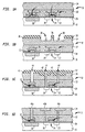
- FIGS. 1A-1G are diagrammatical cross sectional sketches of a semiconductor integrated circuit having an active device and fuse at various stages in the fabrication of such circuit.
- a method is shown forming a semiconductor integrated circuit 10 having a fuse 12 and an active device 14.
- the method includes forming the fuse 12, here an electrically blowable, fuse and the active device 14, here a MOSFET, in different regions of a semiconductor substrate 16 using conventional processing.
- the regions for the fuse 12 and the active device 14 are electrically isolated by silicon dioxide, here by a shallow trench silicon dioxide region 18.
- the active device is, as noted above, a MOSFET having source and drain regions 20, 22, respectively, and a gate region 24 therebetween.
- the fuse 12 is formed over the silicon dioxide shallow trench isolation region 18, as indicated.
- a conformal second layer of silicon nitride is deposited over the structure. Portions of the second silicon nitride layer are removed with a reactive ion etch with portions of the second silicon nitride layer remaining on the sidewalls of the gate electrode to form sidewall spacers in a conventional manner.
- the first deposited silicon nitride layer forms a cap nitride 30 and the second silicon nitride layer forms sidewall spacers 31.
- a dielectric layer 32 here borophosphoro silicate glass (BPSG) is deposited over the gate stack 25 and over the fuse 12, reflowed, planarized with a chemical mechanical polishing process, followed by a dielectric layer 34 of here TEOS.
- BPSG borophosphoro silicate glass
- a photoresist layer 36 is formed over the surface of the dielectric layer 34 and is patterned as shown using conventional photolithography to have openings 38 formed therein, as shown in FIG. 1B.
- the patterned photoresist layer 36 is used as an etch mask to enable formation of trenches 40 in the upper surface portion of the dielectric layer 34, as shown. It is noted that the trenches 34 are aligned over the source and drain regions 20, 22.
- the photoresist mask 36 (FIG. 1B) is removed and replaced with another photoresist layer 42.
- the photoresist layer 42 is patterned as show to enable etching of via holes 44 through the exposed underlying portions of the dielectric layers 34, 32 and the silicon dioxide gate oxide layer 28 over the source and drain regions 20, 22, as indicated.
- via holes 44 are formed through selected regions of the dielectric layers 32, 34 exposing underlying portions of the fuse 12 and underlying portions of a source/drain contact region 20, 22 of the MOSFET active device 14. It should be noted that the via holes 44 may be formed prior to the formation of the trenches 40.
- the photoresist layer 42 (FIG. 1C) is removed and an electrically conductive material 40a, 40b, 40c, here tungsten, is deposited over the surface of the dielectric layer 34. It is noted that the electrically conductive material 46a, 46b, 46c is deposited through the via holes 44 and into the trenches 38 (FIG. 1B), as indicated. The upper portions of the electrically conductive material 46a, 46b, 46c, not shown, are removed using any process, such as chemical mechanical polishing (CMP) to form a planar surface as indicated in FIG. 1D.
- CMP chemical mechanical polishing
- a dual damascene process is used to form the source/drain contacts 46b, 46c and that simultaneously therewith the same material 46a is deposited onto the fuse 12. It is also noted that the portions 46a of the tungsten deposited onto the fuse 12 are electrically isolated from the source/drain electrical contact portions 46b, 46c by portions of the dielectric layers, 32, 34, as indicated.
- a dielectric layer 48 here TEOS, is deposited over the surface of the structure, i.e., on the dielectric layer 34 and over upper portions of tungsten material 46a, 46b, 46c, as shown.
- the dielectric layer 48 is patterned in a manner similar to that used to patter the dielectric layer 48. Here, however, trenches and via holes are aligned with the source and drain electrical contacts provided by the tungsten material 46b, 46c, as indicated.
- a dielectric layer 52 here TEOS is deposited over the surface of the structure shown in FIG. 1E.
- the dielectric layer 52 is patterned in a manner similar to that described in connection with FIGS. 1B and 1C.
- trenches 59 are formed in dielectric layer 52 as shown along with via holes 56a, 56b.
- One via hole, here via hole 56a is aligned over the fuse 12 and another one of the via holes, here via hole 56b, is aligned over a portion of one of the source/drain electrical contacts, here over a portion of drain electrical contact 46c.
- a wet etch here hydrogen peroxide, is brought into contact with the dielectric layer 52, to the exposed tungsten material 46a deposited onto the fuse 12, and to the exposed portion of drain electrical contact 46c.
- the drain electrical contact 46c is of a material different from the material on the fuse 12, i.e., the former being aluminum and the latter being tungsten.
- the hydrogen peroxide selectively removes tungsten material 46a (FIG. 1E) without substantial etching of the dielectric TEOS or BPSG layers 52, 48, 34, 32 or the aluminum material 46c.
- FIG. 1E The resulting structure, after the hydrogen peroxide etch, is shown in FIG.
- an exposed portion of the silicon nitride layer 30 is removed from an upper portion of the tungsten silicide layer 28 over fuse 12.
- Some portions of the tungsten silicide may be removed with the hydrogen peroxide. It is noted that removal of the more electrically conductive tungsten silicide results in a more resistive fuse 12 thereby facilitating in the blowing of such fuse when current passes through the doped polycrystalline silicon 26.
- the sidewall spacers 31 (FIG. 1B) of the silicon nitride may be removed using a chemical dry isotropic, fluoride containing etch to increase the size of the cavity (i.e., the size of the space 64).
- a second metalization layer 60a, 60b, 60c, here aluminum is deposited over the surface of the structure shown in FIG. 1F and then planarized using, for example, CMP, to produce the structure shown in FIG. 1G.
- the aluminum 60a in the via hole 56a over the fuse 12 acts as a fill material.
- the fill material 60a has a bottom portion 62 vertically spaced from the upper surface of the fuse 12. This space 64 thus provides a cavity for fuse material after the fuse 12 is blown.
Landscapes
- Design And Manufacture Of Integrated Circuits (AREA)
- Internal Circuitry In Semiconductor Integrated Circuit Devices (AREA)
- Semiconductor Memories (AREA)
Applications Claiming Priority (2)
| Application Number | Priority Date | Filing Date | Title |
|---|---|---|---|
| US105107 | 1988-01-29 | ||
| US09/105,107 US6261937B1 (en) | 1998-06-24 | 1998-06-24 | Method for forming a semiconductor fuse |
Publications (3)
| Publication Number | Publication Date |
|---|---|
| EP0967638A2 true EP0967638A2 (fr) | 1999-12-29 |
| EP0967638A3 EP0967638A3 (fr) | 2000-11-22 |
| EP0967638B1 EP0967638B1 (fr) | 2006-07-26 |
Family
ID=22304059
Family Applications (1)
| Application Number | Title | Priority Date | Filing Date |
|---|---|---|---|
| EP99110468A Expired - Lifetime EP0967638B1 (fr) | 1998-06-24 | 1999-05-31 | Fusible pour semi-conducteur |
Country Status (7)
| Country | Link |
|---|---|
| US (1) | US6261937B1 (fr) |
| EP (1) | EP0967638B1 (fr) |
| JP (1) | JP2000040746A (fr) |
| KR (1) | KR100609544B1 (fr) |
| CN (1) | CN1143378C (fr) |
| DE (1) | DE69932472T2 (fr) |
| TW (1) | TW432665B (fr) |
Cited By (1)
| Publication number | Priority date | Publication date | Assignee | Title |
|---|---|---|---|---|
| KR100413582B1 (ko) * | 2001-06-28 | 2003-12-31 | 동부전자 주식회사 | 반도체소자용 패드레이어/퓨즈레이어의 형성방법 |
Families Citing this family (21)
| Publication number | Priority date | Publication date | Assignee | Title |
|---|---|---|---|---|
| US6277674B1 (en) * | 1998-10-02 | 2001-08-21 | Micron Technology, Inc. | Semiconductor fuses, methods of using the same, methods of making the same, and semiconductor devices containing the same |
| US6268638B1 (en) * | 1999-02-26 | 2001-07-31 | International Business Machines Corporation | Metal wire fuse structure with cavity |
| US6972612B2 (en) * | 1999-06-22 | 2005-12-06 | Samsung Electronics Co., Ltd. | Semiconductor device with malfunction control circuit and controlling method thereof |
| US6472253B1 (en) * | 1999-11-15 | 2002-10-29 | Vlsi Technology, Inc. | Programmable semiconductor device structures and methods for making the same |
| US6295721B1 (en) * | 1999-12-28 | 2001-10-02 | Taiwan Semiconductor Manufacturing Company | Metal fuse in copper dual damascene |
| KR100400033B1 (ko) * | 2001-02-08 | 2003-09-29 | 삼성전자주식회사 | 다층 배선 구조를 갖는 반도체 소자 및 그의 제조방법 |
| US6458691B1 (en) * | 2001-04-04 | 2002-10-01 | Advanced Micro Devices, Inc. | Dual inlaid process using an imaging layer to protect via from poisoning |
| US6589711B1 (en) | 2001-04-04 | 2003-07-08 | Advanced Micro Devices, Inc. | Dual inlaid process using a bilayer resist |
| KR100444722B1 (ko) * | 2002-04-08 | 2004-08-16 | 아남반도체 주식회사 | 퓨즈 라인 제조 방법 |
| KR100620705B1 (ko) * | 2004-12-31 | 2006-09-13 | 동부일렉트로닉스 주식회사 | 유전체의 두께가 균일한 안티퓨즈 및 그 제조 방법 |
| KR100621773B1 (ko) * | 2005-02-07 | 2006-09-14 | 삼성전자주식회사 | 전기적 퓨즈 회로 및 레이아웃 방법 |
| JP5139689B2 (ja) * | 2007-02-07 | 2013-02-06 | セイコーインスツル株式会社 | 半導体装置とその製造方法 |
| US7983024B2 (en) * | 2007-04-24 | 2011-07-19 | Littelfuse, Inc. | Fuse card system for automotive circuit protection |
| JP2009004565A (ja) * | 2007-06-21 | 2009-01-08 | Nec Electronics Corp | 半導体装置及び半導体装置の製造方法 |
| US8232190B2 (en) * | 2007-10-01 | 2012-07-31 | International Business Machines Corporation | Three dimensional vertical E-fuse structures and methods of manufacturing the same |
| CN102549737B (zh) * | 2009-08-27 | 2014-09-24 | 松下电器产业株式会社 | 半导体装置及其制造方法 |
| US8630108B2 (en) | 2011-03-31 | 2014-01-14 | International Business Machines Corporation | MOSFET fuse and array element |
| CN103094095B (zh) * | 2011-10-28 | 2015-10-21 | 中芯国际集成电路制造(北京)有限公司 | 制造半导体器件的方法 |
| US9070687B2 (en) | 2013-06-28 | 2015-06-30 | Taiwan Semiconductor Manufacturing Co., Ltd. | Semiconductor device with self-protecting fuse |
| US10079156B2 (en) * | 2014-11-07 | 2018-09-18 | Advanced Semiconductor Engineering, Inc. | Semiconductor package including dielectric layers defining via holes extending to component pads |
| US20230402369A1 (en) * | 2022-06-08 | 2023-12-14 | Intel Corporation | Interconnect via metal-insulator-metal (mim) fuse for integrated circuitry |
Family Cites Families (7)
| Publication number | Priority date | Publication date | Assignee | Title |
|---|---|---|---|---|
| JPS5833865A (ja) * | 1981-08-24 | 1983-02-28 | Toshiba Corp | 半導体記憶装置及びその製造方法 |
| JPH02106968A (ja) * | 1988-10-17 | 1990-04-19 | Hitachi Ltd | 半導体集積回路装置及びその形成方法 |
| US5550399A (en) * | 1994-11-03 | 1996-08-27 | Kabushiki Kaisha Toshiba | Integrated circuit with windowed fuse element and contact pad |
| JPH09153552A (ja) * | 1995-11-29 | 1997-06-10 | Mitsubishi Electric Corp | 半導体装置およびその製造方法 |
| DE19600398C1 (de) * | 1996-01-08 | 1997-03-27 | Siemens Ag | Schmelzsicherung in einer integrierten Halbleiterschaltung, deren Verwendung in einer Speicherzelle (PROM) sowie Verfahren zu ihrer Herstellung |
| US5970346A (en) * | 1997-09-19 | 1999-10-19 | Taiwan Semiconductor Manufacturing Company, Ltd. | Fuse window guard ring structure for nitride capped self aligned contact processes |
| US5989784A (en) * | 1998-04-06 | 1999-11-23 | Taiwan Semiconductor Manufacturing Company, Ltd. | Etch recipe for embedded DRAM passivation with etch stopping layer scheme |
-
1998
- 1998-06-24 US US09/105,107 patent/US6261937B1/en not_active Expired - Lifetime
-
1999
- 1999-05-31 DE DE69932472T patent/DE69932472T2/de not_active Expired - Lifetime
- 1999-05-31 EP EP99110468A patent/EP0967638B1/fr not_active Expired - Lifetime
- 1999-06-16 TW TW088110086A patent/TW432665B/zh not_active IP Right Cessation
- 1999-06-23 KR KR1019990023670A patent/KR100609544B1/ko not_active Expired - Fee Related
- 1999-06-24 CN CNB991089154A patent/CN1143378C/zh not_active Expired - Fee Related
- 1999-06-24 JP JP11178936A patent/JP2000040746A/ja not_active Withdrawn
Cited By (1)
| Publication number | Priority date | Publication date | Assignee | Title |
|---|---|---|---|---|
| KR100413582B1 (ko) * | 2001-06-28 | 2003-12-31 | 동부전자 주식회사 | 반도체소자용 패드레이어/퓨즈레이어의 형성방법 |
Also Published As
| Publication number | Publication date |
|---|---|
| JP2000040746A (ja) | 2000-02-08 |
| EP0967638B1 (fr) | 2006-07-26 |
| KR100609544B1 (ko) | 2006-08-04 |
| DE69932472D1 (de) | 2006-09-07 |
| DE69932472T2 (de) | 2007-02-15 |
| US6261937B1 (en) | 2001-07-17 |
| EP0967638A3 (fr) | 2000-11-22 |
| CN1143378C (zh) | 2004-03-24 |
| CN1241810A (zh) | 2000-01-19 |
| TW432665B (en) | 2001-05-01 |
| KR20000006377A (ko) | 2000-01-25 |
Similar Documents
| Publication | Publication Date | Title |
|---|---|---|
| US6261937B1 (en) | Method for forming a semiconductor fuse | |
| US6476488B1 (en) | Method for fabricating borderless and self-aligned polysilicon and metal contact landing plugs for multilevel interconnections | |
| US6583002B2 (en) | Semiconductor processing methods of forming integrated circuitry memory devices, methods of forming capacitor containers, methods of making electrical connection to circuit nodes and related integrated circuitry | |
| US7279419B2 (en) | Formation of self-aligned contact plugs | |
| US6809397B2 (en) | Fuse boxes with guard rings for integrated circuits and integrated circuits including the same | |
| CN114068552A (zh) | 半导体器件以及制造该半导体器件的方法 | |
| US6781182B2 (en) | Interconnect line selectively isolated from an underlying contact plug | |
| US20040262769A1 (en) | Semiconductor device and method of manufacturing the same | |
| US7491603B2 (en) | Transistors of semiconductor device having channel region in a channel-portion hole and methods of forming the same | |
| US7056823B2 (en) | Backend metallization method and device obtained therefrom | |
| US6716756B2 (en) | Method for forming capacitor of semiconductor device | |
| TWI779462B (zh) | 製造半導體結構的方法 | |
| KR100592581B1 (ko) | 집적 회로용 콘택의 제조 방법 및 상기 콘택을 가진반도체 소자 | |
| US11107730B1 (en) | Method of manufacturing semiconductor device with anti-fuse structures | |
| HK1022045A (en) | Semiconductor fuse | |
| US20050026412A1 (en) | Interconnect line selectively isolated from an underlying contact plug | |
| KR20000065823A (ko) | 반도체 메모리 장치의 비트 라인 구조 | |
| KR100506050B1 (ko) | 반도체소자의 콘택 형성방법 | |
| KR20010021422A (ko) | 반도체메모리장치 및 그 제조방법 | |
| KR19990086262A (ko) | 디램 셀 커패시터의 제조 방법 |
Legal Events
| Date | Code | Title | Description |
|---|---|---|---|
| PUAI | Public reference made under article 153(3) epc to a published international application that has entered the european phase |
Free format text: ORIGINAL CODE: 0009012 |
|
| AK | Designated contracting states |
Kind code of ref document: A2 Designated state(s): DE FR GB IE IT NL |
|
| AX | Request for extension of the european patent |
Free format text: AL;LT;LV;MK;RO;SI |
|
| PUAL | Search report despatched |
Free format text: ORIGINAL CODE: 0009013 |
|
| AK | Designated contracting states |
Kind code of ref document: A3 Designated state(s): AT BE CH CY DE DK ES FI FR GB GR IE IT LI LU MC NL PT SE |
|
| AX | Request for extension of the european patent |
Free format text: AL;LT;LV;MK;RO;SI |
|
| 17P | Request for examination filed |
Effective date: 20001216 |
|
| AKX | Designation fees paid |
Free format text: DE FR GB IE IT NL |
|
| RAP1 | Party data changed (applicant data changed or rights of an application transferred) |
Owner name: INFINEON TECHNOLOGIES AG |
|
| 17Q | First examination report despatched |
Effective date: 20040105 |
|
| GRAP | Despatch of communication of intention to grant a patent |
Free format text: ORIGINAL CODE: EPIDOSNIGR1 |
|
| GRAS | Grant fee paid |
Free format text: ORIGINAL CODE: EPIDOSNIGR3 |
|
| GRAA | (expected) grant |
Free format text: ORIGINAL CODE: 0009210 |
|
| AK | Designated contracting states |
Kind code of ref document: B1 Designated state(s): DE FR GB IE IT NL |
|
| PG25 | Lapsed in a contracting state [announced via postgrant information from national office to epo] |
Ref country code: NL Free format text: LAPSE BECAUSE OF FAILURE TO SUBMIT A TRANSLATION OF THE DESCRIPTION OR TO PAY THE FEE WITHIN THE PRESCRIBED TIME-LIMIT Effective date: 20060726 Ref country code: IT Free format text: LAPSE BECAUSE OF FAILURE TO SUBMIT A TRANSLATION OF THE DESCRIPTION OR TO PAY THE FEE WITHIN THE PRESCRIBED TIME-LIMIT;WARNING: LAPSES OF ITALIAN PATENTS WITH EFFECTIVE DATE BEFORE 2007 MAY HAVE OCCURRED AT ANY TIME BEFORE 2007. THE CORRECT EFFECTIVE DATE MAY BE DIFFERENT FROM THE ONE RECORDED. Effective date: 20060726 |
|
| REG | Reference to a national code |
Ref country code: GB Ref legal event code: FG4D |
|
| REG | Reference to a national code |
Ref country code: IE Ref legal event code: FG4D |
|
| REF | Corresponds to: |
Ref document number: 69932472 Country of ref document: DE Date of ref document: 20060907 Kind code of ref document: P |
|
| NLV1 | Nl: lapsed or annulled due to failure to fulfill the requirements of art. 29p and 29m of the patents act | ||
| REG | Reference to a national code |
Ref country code: HK Ref legal event code: WD Ref document number: 1022045 Country of ref document: HK |
|
| ET | Fr: translation filed | ||
| PLBE | No opposition filed within time limit |
Free format text: ORIGINAL CODE: 0009261 |
|
| STAA | Information on the status of an ep patent application or granted ep patent |
Free format text: STATUS: NO OPPOSITION FILED WITHIN TIME LIMIT |
|
| 26N | No opposition filed |
Effective date: 20070427 |
|
| GBPC | Gb: european patent ceased through non-payment of renewal fee |
Effective date: 20070531 |
|
| PG25 | Lapsed in a contracting state [announced via postgrant information from national office to epo] |
Ref country code: IE Free format text: LAPSE BECAUSE OF NON-PAYMENT OF DUE FEES Effective date: 20070531 Ref country code: GB Free format text: LAPSE BECAUSE OF NON-PAYMENT OF DUE FEES Effective date: 20070531 |
|
| REG | Reference to a national code |
Ref country code: FR Ref legal event code: TP Owner name: QIMONDA AG,, DE Effective date: 20120123 |
|
| PGFP | Annual fee paid to national office [announced via postgrant information from national office to epo] |
Ref country code: DE Payment date: 20140619 Year of fee payment: 16 |
|
| REG | Reference to a national code |
Ref country code: FR Ref legal event code: PLFP Year of fee payment: 17 |
|
| REG | Reference to a national code |
Ref country code: DE Ref legal event code: R081 Ref document number: 69932472 Country of ref document: DE Owner name: POLARIS INNOVATIONS LTD., IE Free format text: FORMER OWNER: QIMONDA AG, 81739 MUENCHEN, DE Ref country code: DE Ref legal event code: R081 Ref document number: 69932472 Country of ref document: DE Owner name: INFINEON TECHNOLOGIES AG, DE Free format text: FORMER OWNER: QIMONDA AG, 81739 MUENCHEN, DE |
|
| PGFP | Annual fee paid to national office [announced via postgrant information from national office to epo] |
Ref country code: IT Payment date: 20150514 Year of fee payment: 17 Ref country code: FR Payment date: 20150521 Year of fee payment: 17 |
|
| REG | Reference to a national code |
Ref country code: DE Ref legal event code: R081 Ref document number: 69932472 Country of ref document: DE Owner name: POLARIS INNOVATIONS LTD., IE Free format text: FORMER OWNER: INFINEON TECHNOLOGIES AG, 85579 NEUBIBERG, DE |
|
| REG | Reference to a national code |
Ref country code: DE Ref legal event code: R119 Ref document number: 69932472 Country of ref document: DE |
|
| REG | Reference to a national code |
Ref country code: FR Ref legal event code: TP Owner name: INFINEON TECHNOLOGIES AG, DE Effective date: 20160212 |
|
| PG25 | Lapsed in a contracting state [announced via postgrant information from national office to epo] |
Ref country code: DE Free format text: LAPSE BECAUSE OF NON-PAYMENT OF DUE FEES Effective date: 20151201 |
|
| PG25 | Lapsed in a contracting state [announced via postgrant information from national office to epo] |
Ref country code: IT Free format text: LAPSE BECAUSE OF NON-PAYMENT OF DUE FEES Effective date: 20160531 |
|
| REG | Reference to a national code |
Ref country code: FR Ref legal event code: ST Effective date: 20170131 |
|
| PG25 | Lapsed in a contracting state [announced via postgrant information from national office to epo] |
Ref country code: FR Free format text: LAPSE BECAUSE OF NON-PAYMENT OF DUE FEES Effective date: 20160531 |