EP0967661A2 - Dispositifs photodétecteur réceptifs sur le bord - Google Patents
Dispositifs photodétecteur réceptifs sur le bord Download PDFInfo
- Publication number
- EP0967661A2 EP0967661A2 EP99303687A EP99303687A EP0967661A2 EP 0967661 A2 EP0967661 A2 EP 0967661A2 EP 99303687 A EP99303687 A EP 99303687A EP 99303687 A EP99303687 A EP 99303687A EP 0967661 A2 EP0967661 A2 EP 0967661A2
- Authority
- EP
- European Patent Office
- Prior art keywords
- region
- light
- edge
- waveguide
- circuit according
- Prior art date
- Legal status (The legal status is an assumption and is not a legal conclusion. Google has not performed a legal analysis and makes no representation as to the accuracy of the status listed.)
- Withdrawn
Links
Images

Classifications
-
- H—ELECTRICITY
- H10—SEMICONDUCTOR DEVICES; ELECTRIC SOLID-STATE DEVICES NOT OTHERWISE PROVIDED FOR
- H10F—INORGANIC SEMICONDUCTOR DEVICES SENSITIVE TO INFRARED RADIATION, LIGHT, ELECTROMAGNETIC RADIATION OF SHORTER WAVELENGTH OR CORPUSCULAR RADIATION
- H10F77/00—Constructional details of devices covered by this subclass
- H10F77/40—Optical elements or arrangements
-
- G—PHYSICS
- G02—OPTICS
- G02B—OPTICAL ELEMENTS, SYSTEMS OR APPARATUS
- G02B6/00—Light guides; Structural details of arrangements comprising light guides and other optical elements, e.g. couplings
- G02B6/24—Coupling light guides
- G02B6/42—Coupling light guides with opto-electronic elements
-
- G—PHYSICS
- G02—OPTICS
- G02B—OPTICAL ELEMENTS, SYSTEMS OR APPARATUS
- G02B6/00—Light guides; Structural details of arrangements comprising light guides and other optical elements, e.g. couplings
- G02B6/24—Coupling light guides
- G02B6/42—Coupling light guides with opto-electronic elements
- G02B6/4201—Packages, e.g. shape, construction, internal or external details
- G02B6/4246—Bidirectionally operating package structures
-
- H—ELECTRICITY
- H10—SEMICONDUCTOR DEVICES; ELECTRIC SOLID-STATE DEVICES NOT OTHERWISE PROVIDED FOR
- H10F—INORGANIC SEMICONDUCTOR DEVICES SENSITIVE TO INFRARED RADIATION, LIGHT, ELECTROMAGNETIC RADIATION OF SHORTER WAVELENGTH OR CORPUSCULAR RADIATION
- H10F77/00—Constructional details of devices covered by this subclass
- H10F77/40—Optical elements or arrangements
- H10F77/407—Optical elements or arrangements indirectly associated with the devices
Definitions
- This invention relates to photodetector devices, and in particular to edge receptive semiconductor photodetector devices, as well as lightguide circuits incorporating the photodetectors.
- Certain optical transmitters and receivers such as planar lightguide circuits, require that PIN photodiodes be utilized for light detection. Since such diodes tend to be face-receptive, i.e., the light must be incident on one of the major surfaces of the diode, a turning mirror is generally used to direct the light from an in-plane waveguide to the PIN diode. Fabrication of the turning mirror tends to be difficult and time consuming, and can add considerable cost to the lightguide circuit.
- the invention in one aspect is a photodetector device which includes multiple regions of semiconductor material which form an edge surface of the device.
- the device is adapted to receive light on the edge surface, absorb the light, and to generate carriers in the semiconductor material in response thereto to produce a current which is proportional to the intensity of the incident light.
- a region of the device has a shape which is narrow at the edge receiving the light and fans out in the direction of light propagation in the device.
- the invention is a lightguide circuit which includes a substrate including a waveguide formed on a surface thereof, the substrate including at least one well formed on one edge of the substrate, a semiconductor laser mounted in the well and aligned with a portion of the waveguide, and a semiconductor device also mounted in the same or another well and aligned with another portion of the waveguide.
- the device comprises multiple regions of semiconductor material forming an edge surface of the device, the device being adapted to receive light from the waveguide on said edge surface, absorb the light, and to generate carriers in the semiconductor material in response thereto to produce a current which is proportional to the intensity of the incident light.
- a region of the device has a shape which is narrow at the edge and fans out in the direction of light propagation in the device.
- Fig 1 illustrates a typical optical transmitter, 10, incorporating features of the invention.
- the transmitter includes a substrate, 11, which is typically silicon.
- a dielectric layer, 12, which is typically Si0 2 is formed on the substrate 11.
- a waveguide, 16, is formed within the dielectric layer 12 by causing portions of the layer to be doped so as to produce an appropriately varying refractive index.
- Typical dopants are Boron and/or Phosphorous, and the waveguide may be produced, for example, by depositing first a layer of undoped Si0 2 and then a layer of Phosphorous doped Si0 2 followed by patterning the phosphorous doped layer photolithography to define the waveguide core.
- a top cladding layer is deposited over the core, which top layer is doped with both Boron and Phosphorous.
- a well or wells (13, for the case of a single common well) is etched into the dielectric layer, down to the substrate.
- a laser, 14, is bonded to the substrate at the bottom of the well, so that its axis of light emission aligns with the waveguide core.
- An edge receptive photodetector device, 15, to be further described, is also bonded to the substrate at the bottom of the well 13, so that its axis for light reception aligns with the core of the waveguide.
- the waveguide 16 includes ports 17 and 18 for the purpose of aligning with the laser 14 and the detector 15, and also includes a port 19 which is aligned with an optical fiber 20.
- Other devices, such as optical isolators may also be on the same substrate.
- edge-receptive photodetector 15
- the photodetector allows the photodetector to receive light directly from the waveguide, without the need for a turning mirror which would be necessary if a face receptive detector were employed.
- the well or wells for mounting the laser and detector may be etched in a single photolithographic step, and the need for a separate etching step to define turning mirrors is not required.
- the turning mirror fabrication usually requires the simultaneous etching of a vertical wall to terminate the waveguide core and a nominally 45 degree surface to reflect the light upwards to the face receptive detector - a technologically challenging step which is not compatible with standard photolithography and requires a "gray-scale” mask or a differently erodable, undercutting masking layer, either of which are considerably more complex than the use of conventionally patterned resists and "black or white” masks.
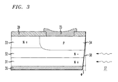
- Figs 2 and 3 illustrate one embodiment of an edge receptive photodetector, 15, in accordance with the invention.
- Fig 2 is a plan view of the device
- Fig. 3 is a cross sectional view along section 2-2 (through the axis).
- the photodetector includes a first region , 31, (e.g., a substrate) of semiconductor material having a first conductivity type, which in this example is N+ type.
- This region can be, for example, InP doped with Silicon or Sn to a concentration giving 2x10 18 electrons per cubic cm.
- a second region, 32 is formed on top of this first region by, for example, vapor phase epitaxy.
- This layer may be InGaAs or InGaAsP, having a bandgap such that the light of interest can be absorbed and converted to electron/hole pairs.
- This layer is typically not doped with impurities and is intrinsic-n-type with a background electron concentration of 5x10 15 per cubic cm or less.
- a third region of N+ type InP (33) is formed, accomplished by vapor phase epitaxy as described above for layer 32. This layer is typically doped to a concentration of 2 x 10 17 cm -3 .
- a p-type conductivity region 34 is then formed into the topmost layer 33 by ion implantation or diffusion of an acceptor species, such as Zn.
- This region is defined by an appropriate diffusion or implant mask, which is photolithography patterned so that region 34 is formed into a fan shape as shown schematically in figure 2.
- the depth of the implant or diffusion is controlled so as to type convert the upper N+ InP layer 33 and so that a P/N-intrinsic junction results between the implanted region 34 and the intrinsic InGaAsP or InGaAs layer 32.
- the mask is typically stripped off, and a new dielectric layer 39, is deposited and patterned on the surface of regions 33 and 34.
- a p-contact metallization 35 is formed contacting the region 34, and an n-contact (36) is formed either to the first region 31 at the back side, or to the top layer 33 outside the region 34.
- These contact metallizations constitute standard electrodes allowing for the biasing and electrical connection of the device to external circuitry and the methods for their preparation are well known in the art.
- edge 38 of the device In operation light represented by the arrows 37 is incident on the edge 38 of the device.
- This edge is typically formed by cleaving the InP material constituting the first region 31 on a (110) plane. If the deposition of the second region 32 took place conventionally on a 2 degree off-oriented surface, this cleaved edge may be selected to be 2 degrees away from the perpendicular to the planes of the device layers as shown by angle ⁇ in figure 3.
- the light 37 upon entering the device will then be refracted upwards toward the absorbing layer 32 and the reflecting contact, 35, that will reflect light back down to the absorbing layer, and this is beneficial.
- epitaxial growth may be performed on a surface oriented more than 2 degree off the (100) surface, and, consequently, the angle, ⁇ , may be increased to enhance the refraction of light toward the absorbing layer 32 and hence further enhanced the quantum efficiency.
- angle ⁇ is preferably 4-5 degrees.
- FIG. 3 shows the device with the contact layer (34) at the top, it is conventional in actual use to mount the device with the p-contact down, facing the board to which it is mounted.
- the light will be guided along the absorbing layer owing to the higher refractive index of the layer 32, and will be absorbed as it propagates into the device. In the plane of the absorbing layer there is no waveguiding and the light will spread out by diffraction. Depending on the light beam spot size exiting the waveguide port 18 this spreading angle will vary, but is typically between 10 and 50 degrees full angle for typical waveguide ports. The spreading angle within the device will of course be less than that which would have been observed had the beam been allowed to expand freely into the air.
- the edge surface of the device 38 is provided with an antireflective coating (not shown) so that the light enters into the device and is not reflected back toward the waveguide port 18.
- the dimensions of the p-region 34 are chosen in relation to the thickness and composition of the absorbing region 32 and with regard to the desired quantum efficiency and speed of operation of the device.
- the fan angle, ⁇ should be large enough so that the light, as it spreads within the device in the plane of the layer 32, does not spread outside of the region underlying 34. In general, angles of 1-50 degrees will be used, with a preferred range of 10-50 degrees.
- the initial width W of the region 34 should be such that the light beam enters entirely within the region underlying 34. This may be, for example, 10 ⁇ m corresponding to a waveguide port with a core width of 7 ⁇ m and an allowance for alignment tolerance of +/- 1.5 ⁇ m.
- the width W will be 2-25 microns, and the largest width W' will be at least 20 microns.
- the overall length 1 of the region 34 measured down the light propagation axis should be long enough that most or all of the light is absorbed, or at least that sufficient light is absorbed that the design quantum efficiency is met. This length will vary depending upon the composition and thickness of layer 32. In general, a length, 1, of 20-70 ⁇ m is preferred.
- the area of the region 34 determines the area and hence the capacitance of the p-n junction in the device. The capacitance of the p-n junction is one variable determining the limiting speed of operation of the device (the lower the capacitance the faster) and it is desirable to reduce the area accordingly unless other parameters have become the limiting factor.
- the area of the region 34 should not be too small, as the photocurrent density must be limited to an upper limit, typically 1x10 5 amp/cm 2 . If the junction area is too small, this will restrict the maximum photocurrent and hence light signal, and will limit the useful dynamic range. It should also be arranged that the light spreads through the intended absorption region and is not absorbed too precipitously.
Landscapes
- Physics & Mathematics (AREA)
- General Physics & Mathematics (AREA)
- Optics & Photonics (AREA)
- Light Receiving Elements (AREA)
- Optical Integrated Circuits (AREA)
Applications Claiming Priority (2)
| Application Number | Priority Date | Filing Date | Title |
|---|---|---|---|
| US83496 | 1979-10-10 | ||
| US09/083,496 US6064782A (en) | 1998-05-22 | 1998-05-22 | Edge receptive photodetector devices |
Publications (2)
| Publication Number | Publication Date |
|---|---|
| EP0967661A2 true EP0967661A2 (fr) | 1999-12-29 |
| EP0967661A3 EP0967661A3 (fr) | 2000-04-26 |
Family
ID=22178724
Family Applications (1)
| Application Number | Title | Priority Date | Filing Date |
|---|---|---|---|
| EP99303687A Withdrawn EP0967661A3 (fr) | 1998-05-22 | 1999-05-12 | Dispositifs photodétecteur réceptifs sur le bord |
Country Status (3)
| Country | Link |
|---|---|
| US (1) | US6064782A (fr) |
| EP (1) | EP0967661A3 (fr) |
| JP (1) | JPH11345996A (fr) |
Families Citing this family (3)
| Publication number | Priority date | Publication date | Assignee | Title |
|---|---|---|---|---|
| JP2003021723A (ja) * | 2001-07-06 | 2003-01-24 | Photonixnet Corp | モードカットフィルタ及び光送受信機 |
| US20050019037A1 (en) * | 2003-07-25 | 2005-01-27 | Luo Xin Simon | To can laser package with front monitoring photodetector and turning mirror |
| US7773836B2 (en) | 2005-12-14 | 2010-08-10 | Luxtera, Inc. | Integrated transceiver with lightpipe coupler |
Family Cites Families (6)
| Publication number | Priority date | Publication date | Assignee | Title |
|---|---|---|---|---|
| JP2710070B2 (ja) * | 1989-09-20 | 1998-02-10 | 松下電子工業株式会社 | 半導体受光素子及びこの半導体受光素子を用いた光半導体装置 |
| DE69129311T2 (de) * | 1990-02-26 | 1998-10-08 | Canon Kk | Photodetektor |
| KR0126247B1 (en) * | 1992-11-09 | 1997-12-26 | Fujitsu Ltd | Method of coupling optical parts and refractive index imaging material |
| US5912500A (en) * | 1995-11-22 | 1999-06-15 | Intevac, Inc. | Integrated photocathode |
| JP3276836B2 (ja) * | 1996-02-16 | 2002-04-22 | 日本電信電話株式会社 | 半導体導波路型受光器 |
| JP2748917B2 (ja) * | 1996-03-22 | 1998-05-13 | 日本電気株式会社 | 半導体装置 |
-
1998
- 1998-05-22 US US09/083,496 patent/US6064782A/en not_active Expired - Lifetime
-
1999
- 1999-05-12 EP EP99303687A patent/EP0967661A3/fr not_active Withdrawn
- 1999-05-21 JP JP11140891A patent/JPH11345996A/ja active Pending
Also Published As
| Publication number | Publication date |
|---|---|
| US6064782A (en) | 2000-05-16 |
| EP0967661A3 (fr) | 2000-04-26 |
| JPH11345996A (ja) | 1999-12-14 |
Similar Documents
| Publication | Publication Date | Title |
|---|---|---|
| KR100306414B1 (ko) | 광검출기 | |
| US5121182A (en) | Integrated optical semiconductor device | |
| JP3221916B2 (ja) | 集積型光学ガイドと、光検出器とを備えたオプトエレクトロニックデバイス | |
| KR101037998B1 (ko) | 내부 반사기를 구비한 반도체 광검출기 | |
| US5190883A (en) | Method for making an integrated light guide detector structure made of a semiconductive material | |
| US5521994A (en) | Semiconductor optical waveguide-integrated light-receiving device | |
| CN101438419A (zh) | 光电二极管、用于制造这种光电二极管的方法、光学通信设备和光学互连模块 | |
| JPS6329418B2 (fr) | ||
| JPS63224252A (ja) | 導波路−ホトダイオードアレー | |
| KR102307789B1 (ko) | 후면 입사형 애벌런치 포토다이오드 및 그 제조 방법 | |
| KR100464333B1 (ko) | 수광소자 및 그 제조방법 | |
| US6064782A (en) | Edge receptive photodetector devices | |
| JP3589878B2 (ja) | 裏面入射型受光装置およびその作製方法 | |
| JPH06268196A (ja) | 光集積装置 | |
| GB2213957A (en) | Waveguide to opto-electronic transducer coupling | |
| EP0895323A1 (fr) | Laser à réaction distribuée avec couplage de perte | |
| JP2002503825A (ja) | 光学構造体および光学構造体を製造するための方法 | |
| JP2633234B2 (ja) | 光半導体素子 | |
| WO2023062766A1 (fr) | Élément de réception de lumière de type guide d'ondes, réseau d'éléments de réception de lumière de type guide d'ondes, et procédé de production d'élément de réception de lumière de type guide d'ondes | |
| KR19990006160A (ko) | 애벌런치 포토 다이오드 및 그의 제조방법 | |
| JP3224192B2 (ja) | 半導体導波路型受光器 | |
| JP3672168B2 (ja) | 半導体受光装置 | |
| TW202522057A (zh) | 具有凹口光吸收層之光感測器 | |
| JPS6380590A (ja) | 光出力モニタ付半導体レ−ザ | |
| JPH0233982A (ja) | 波長多重弁別型半導体受光素子 |
Legal Events
| Date | Code | Title | Description |
|---|---|---|---|
| PUAI | Public reference made under article 153(3) epc to a published international application that has entered the european phase |
Free format text: ORIGINAL CODE: 0009012 |
|
| AK | Designated contracting states |
Kind code of ref document: A2 Designated state(s): DE FR GB |
|
| AX | Request for extension of the european patent |
Free format text: AL;LT;LV;MK;RO;SI |
|
| PUAL | Search report despatched |
Free format text: ORIGINAL CODE: 0009013 |
|
| AK | Designated contracting states |
Kind code of ref document: A3 Designated state(s): AT BE CH CY DE DK ES FI FR GB GR IE IT LI LU MC NL PT SE |
|
| AX | Request for extension of the european patent |
Free format text: AL;LT;LV;MK;RO;SI |
|
| 17P | Request for examination filed |
Effective date: 20001011 |
|
| AKX | Designation fees paid |
Free format text: DE FR GB |
|
| RAP1 | Party data changed (applicant data changed or rights of an application transferred) |
Owner name: AGERE SYSTEMS OPTOELECTRONICS GUARDIAN CORPORATION |
|
| STAA | Information on the status of an ep patent application or granted ep patent |
Free format text: STATUS: THE APPLICATION IS DEEMED TO BE WITHDRAWN |
|
| 18D | Application deemed to be withdrawn |
Effective date: 20021202 |