EP0967729A2 - Selbstkalibrierung eines AD-Wandlers in einem Bildsensor des CMOS-Typs - Google Patents
Selbstkalibrierung eines AD-Wandlers in einem Bildsensor des CMOS-Typs Download PDFInfo
- Publication number
- EP0967729A2 EP0967729A2 EP99111919A EP99111919A EP0967729A2 EP 0967729 A2 EP0967729 A2 EP 0967729A2 EP 99111919 A EP99111919 A EP 99111919A EP 99111919 A EP99111919 A EP 99111919A EP 0967729 A2 EP0967729 A2 EP 0967729A2
- Authority
- EP
- European Patent Office
- Prior art keywords
- signal
- converter
- output
- converters
- compensation value
- Prior art date
- Legal status (The legal status is an assumption and is not a legal conclusion. Google has not performed a legal analysis and makes no representation as to the accuracy of the status listed.)
- Withdrawn
Links
- 238000000034 method Methods 0.000 claims abstract description 39
- 238000012545 processing Methods 0.000 claims description 27
- 238000005070 sampling Methods 0.000 claims description 27
- 230000000295 complement effect Effects 0.000 claims description 7
- 230000008878 coupling Effects 0.000 claims 2
- 238000010168 coupling process Methods 0.000 claims 2
- 238000005859 coupling reaction Methods 0.000 claims 2
- 230000008569 process Effects 0.000 abstract description 9
- 238000010586 diagram Methods 0.000 description 13
- 238000006243 chemical reaction Methods 0.000 description 11
- 230000003071 parasitic effect Effects 0.000 description 10
- 238000004519 manufacturing process Methods 0.000 description 3
- 230000003287 optical effect Effects 0.000 description 2
- 230000007704 transition Effects 0.000 description 2
- 235000008733 Citrus aurantifolia Nutrition 0.000 description 1
- 101000631701 Homo sapiens Secretin receptor Proteins 0.000 description 1
- 102100028927 Secretin receptor Human genes 0.000 description 1
- 235000011941 Tilia x europaea Nutrition 0.000 description 1
- 238000013459 approach Methods 0.000 description 1
- 238000003491 array Methods 0.000 description 1
- 230000015556 catabolic process Effects 0.000 description 1
- 230000008859 change Effects 0.000 description 1
- 238000006731 degradation reaction Methods 0.000 description 1
- 238000013461 design Methods 0.000 description 1
- 230000000694 effects Effects 0.000 description 1
- 230000010354 integration Effects 0.000 description 1
- 239000004571 lime Substances 0.000 description 1
- 238000012986 modification Methods 0.000 description 1
- 230000004048 modification Effects 0.000 description 1
- 230000036316 preload Effects 0.000 description 1
- 239000004065 semiconductor Substances 0.000 description 1
- 230000035945 sensitivity Effects 0.000 description 1
- 230000001360 synchronised effect Effects 0.000 description 1
Images






Classifications
-
- H—ELECTRICITY
- H03—ELECTRONIC CIRCUITRY
- H03M—CODING; DECODING; CODE CONVERSION IN GENERAL
- H03M1/00—Analogue/digital conversion; Digital/analogue conversion
- H03M1/10—Calibration or testing
- H03M1/1009—Calibration
- H03M1/1014—Calibration at one point of the transfer characteristic, i.e. by adjusting a single reference value, e.g. bias or gain error
- H03M1/1023—Offset correction
-
- H—ELECTRICITY
- H04—ELECTRIC COMMUNICATION TECHNIQUE
- H04N—PICTORIAL COMMUNICATION, e.g. TELEVISION
- H04N25/00—Circuitry of solid-state image sensors [SSIS]; Control thereof
- H04N25/70—SSIS architectures; Circuits associated therewith
- H04N25/76—Addressed sensors, e.g. MOS or CMOS sensors
- H04N25/77—Pixel circuitry, e.g. memories, A/D converters, pixel amplifiers, shared circuits or shared components
- H04N25/772—Pixel circuitry, e.g. memories, A/D converters, pixel amplifiers, shared circuits or shared components comprising A/D, V/T, V/F, I/T or I/F converters
-
- H—ELECTRICITY
- H04—ELECTRIC COMMUNICATION TECHNIQUE
- H04N—PICTORIAL COMMUNICATION, e.g. TELEVISION
- H04N25/00—Circuitry of solid-state image sensors [SSIS]; Control thereof
- H04N25/60—Noise processing, e.g. detecting, correcting, reducing or removing noise
- H04N25/616—Noise processing, e.g. detecting, correcting, reducing or removing noise involving a correlated sampling function, e.g. correlated double sampling [CDS] or triple sampling
-
- H—ELECTRICITY
- H04—ELECTRIC COMMUNICATION TECHNIQUE
- H04N—PICTORIAL COMMUNICATION, e.g. TELEVISION
- H04N25/00—Circuitry of solid-state image sensors [SSIS]; Control thereof
- H04N25/60—Noise processing, e.g. detecting, correcting, reducing or removing noise
- H04N25/67—Noise processing, e.g. detecting, correcting, reducing or removing noise applied to fixed-pattern noise, e.g. non-uniformity of response
-
- H—ELECTRICITY
- H04—ELECTRIC COMMUNICATION TECHNIQUE
- H04N—PICTORIAL COMMUNICATION, e.g. TELEVISION
- H04N25/00—Circuitry of solid-state image sensors [SSIS]; Control thereof
- H04N25/70—SSIS architectures; Circuits associated therewith
- H04N25/76—Addressed sensors, e.g. MOS or CMOS sensors
- H04N25/78—Readout circuits for addressed sensors, e.g. output amplifiers or A/D converters
-
- H—ELECTRICITY
- H03—ELECTRONIC CIRCUITRY
- H03M—CODING; DECODING; CODE CONVERSION IN GENERAL
- H03M1/00—Analogue/digital conversion; Digital/analogue conversion
- H03M1/12—Analogue/digital converters
- H03M1/1205—Multiplexed conversion systems
- H03M1/123—Simultaneous, i.e. using one converter per channel but with common control or reference circuits for multiple converters
-
- H—ELECTRICITY
- H03—ELECTRONIC CIRCUITRY
- H03M—CODING; DECODING; CODE CONVERSION IN GENERAL
- H03M1/00—Analogue/digital conversion; Digital/analogue conversion
- H03M1/12—Analogue/digital converters
- H03M1/50—Analogue/digital converters with intermediate conversion to time interval
- H03M1/56—Input signal compared with linear ramp
-
- H—ELECTRICITY
- H04—ELECTRIC COMMUNICATION TECHNIQUE
- H04N—PICTORIAL COMMUNICATION, e.g. TELEVISION
- H04N25/00—Circuitry of solid-state image sensors [SSIS]; Control thereof
- H04N25/70—SSIS architectures; Circuits associated therewith
- H04N25/76—Addressed sensors, e.g. MOS or CMOS sensors
- H04N25/767—Horizontal readout lines, multiplexers or registers
Definitions
- the present invention relates to a CMOS type image sensor and, in particular, to an initialization procedure of the A/D converters within the CMOS type image sensor.
- An image sensor is used to transform an optical image focused on the an sensor into electrical signal.
- the image sensor typically contains an array of light detecting elements, where each element produces a signal responding to the light intensity impinging on that element when an image is focused on the array. These signals may then be used to display a corresponding image on a monitor.
- CMOS active pixel sensors have attracted much attention recently because of the monolithic integration of control, drive and signal process circuitry upon a single sensor chip.
- CMOS APS imagers are: (1) low voltage operation and low power consumption, (2) process compatibility with on-chip electronics, and (3) potentially lower cost as compared to the conventional CCD, because of the wide availability of a standard CMOS manufacturing process.
- the analog signal generated by each light detecting element is subject to varying degrees of parasitic effects such as those caused by parasitic capacitance, resistance, dark current leakage, or non-uniformity of device characteristics.
- parasitic effects are inherent in semiconductor devices and result in degradation of the signal-to-noise ratio of the image information. Therefore, noise issues pose a major technical challenge which can limit performance of the CMOS APS.
- noises include kTC noise which is associated with the sampling of the image data, l/f noise which is associated with the circuits used to amplify the image signal, and fixed pattern noise which is associated with the non-uniformity between columns within the array.
- An active pixel image sensor fabricated by a CMOS process is described herein which includes a two-dimensional pixel array core of photo sensing diodes whose conductivities are related to the magnitude of light impinging upon the photodiodes.
- the analog signals generated by the photodiodes are buffered through a source follower amplifier, accessed by row transistors and coupled to respective columns in the array.
- the analog signals at each column line are converted to digital signals by an A/D converter (ADC) connected to each column line.
- A/D converter may be formed by a high-gain comparator, an 8-bit binary counter coordinated with a reference ramp signal synchronized with a specific timing sequence.
- a specific timing sequence is used to allow the A/D converter circuit to implement the A/D conversion within a time frame, so that all the sensing elements in a row will have their respective light level converted into a digital value during this interval.
- the timing might allow the resulting digital values to be delivered to another functional block of the chip or off the chip for processing during this time also, or perhaps during another time interval.
- the potential of the input nodes of CDS on each column line is set up to be a "reference" voltage and then its value on each column is convened to a digital value through an A/D converter.
- the resulting output digital data contains information regarding non-uniformity and variation due to the device characteristic variations of A/D converters and CDS circuits.
- the digital data value corresponding to each output line thus obtained is then used to be the initial value of each ADC counter before the following of actual A/D operation on a row of the pixel array is performed.
- major parasitic effects and distortion of the A/D converters and CDS circuits are minimized during subsequent A/D conversions of actual image.
- Figure 1 illustrates the architecture of a 640 x 480 CMOS active pixel image sensor formed on a single integrated circuit chip.
- the image sensor core array 19 comprises a two-dimensional pixel array of light detecting elements each denoted at 10 which include identical circuitry shown in Figure 2.
- a row address shift register 12, with its control signals 152 coming from the timing/control logic 15, is connected to the core array 19 to address one row at one time.
- the output of shift register 12 addresses the core array 19 row-by-row by address lines 21 to read the analog signal into the column lines 14 according to a predetermined frame rate timing requirement.
- each A/D converter 16 is connected to receive an analog signal, via a well known correlated-double sampling (CDS) circuit 18, from corresponding column line 14 and converts each analog signal to a digital signal representative of gray level of light intensity detected by the respective pixel element 10. For example, if an eight-bit A/D conversion is implemented, the analog signal would have 256 values, each representing a level of optical intensity.
- the function of the CDS circuit 18 will be recited hereinafter when Figure 4 is touched upon.
- the timing/control logic 15 outputs timing signals, i.e. switching signals operating the CDS circuit 18, the control signals operating the row address shift register 12, and the signals operating the shift registers 13 to control the operation of the system.
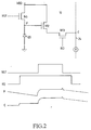
- each light detecting element 10 comprises a photodiode 20, or an equivalent photo sensing device, such as photogate, bipolar phototransistor, etc. whose conducting current is related to the light intensity impinging upon the junction of photo sensing device.
- the internal column line 24 is isolated because the access transistor M3 is turned off due to inactive state of the read signal RD.
- the photodiode 20 is initially reset to a value close to the VDD level by means of the reset transistor M1 which is turned on by the active state of the reset signal RST which is output from the row address shift register 12 of Fig. 1.
- the exposure commences as the reset transistor M1 is turned off by the inactive state of the signal RST. This allows the photodiode current, due to the light impinging on it, to discharge its own inherent capacitance, reducing the charge on node P.
- the access transistors M3 for the row are turned on by an active RD signal. This causes the photodiode voltage at node P, translated through the source follower transistor M2 and the access transistor M3, to be coupled to the internal column line 24.
- the voltage is offset by the effects of the source follower transistor M2, and, of course, will vary with the characteristics of the transistor M2. This voltage is stored in a circuitry at the end of the column line 24.
- the reset transistors M1 in the row are then turned on again, causing the input of the source follower M2, which is coupled to the cathode node P of photodiode 20, to be reset to a value close to the VDD.
- the actual signal sensingd by the following correlated-double sampling (CDS) circuit 18 is the difference of signals at node C, denoted as ⁇ Vc, before and after the reset signal RST is activated.
- the subtraction of the signals of the node C at different moments is accomplished by the well known CDS circuitry and the details of which will not be covered by this invention.
- the signal at the internal column line 24 at different times both contain the offset of the source follower M2 and the access transistor M3, so that error associated thereof is automatically canceled.
- the difference in the signal then is presented to the A/D circuit 16 for conversion to a digital value.
- the actual image capturing operation is done by capturing the difference of signals at column node C respectively at the end of exposure time and after the reset signal RST is activated.
- FIG. 3 shows a functional block diagram of an exemplary A/D converter 16.
- the A/D converter 16 illustrated includes a high gain comparator 32, a clock gating logic 34 and an 8-bit binary counter 36, and two inverters 33, 35.
- a reference ramp signal 38 is input to the non-inverting input node of the comparator 32, and the analog signal 31 from the CDS circuit is input to the inverting input node of the comparator 32.
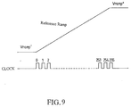
- the clock signal 39 is gated by the output signal of the inverter 33. In performing the A/D conversion, as the reference ramp signal 38 starts to increase and the clock signal 39 starts to tick, the counter 36 starts to count accordingly.
- the output of comparator 32 flips and un-gates the clock signal 39 via the clock gating logic 34.
- the output of the counter 36 when it stops counting, therefore represents the digital value corresponding to the analog signal 31.
- the Vramp- value is the lowest level of the ramp signal 38 and the Vramp+ is the highest level of the ramp signal 38.
- the critical path of the analog signal 31 from input to output includes the source follower M2, the access transistor M3, the internal column line 24, the CDS circuit 18 and the comparator circuit 32 within the A/D converter 16.
- the device variation between the source followers M2 and between access transistors M3 will generate a different signal value on respective internal column lines 24 of each photocell 10.
- the read timings for the pixels in the two successive row lines are exemplarily shown in Figure 5.
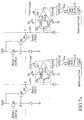
- the S1 and S2 signals respectively operate the switches S1 and S2 in Figure 4.
- a line time period of 69.4 ⁇ s which corresponds to a 30 Hz frame rate with 480 row lines, is disclosed in Figure 5 and will be used later when applicable.
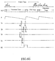
- the invention provides a series of the operations for each column at the beginning of the frame time slot and before the read operation for the first line within each frame.
- the occurrence of the pulses at time t2 and t3 on signals S1, S2 involves the sampling of the actual image signal.
- the present invention in addition to two conventional switches S1, S2, provides two additional switches S3, S4, operated by the corresponding signals S3, S4 shown in Fig. 6(b), to selectively transmit a difference signal.
- each internal column line 24 is pulled down to VL by means of a switch S3.
- This VL voltage is then stored in the inverting input node (SIG) of the differential amplifier 60 of the CDS circuit 18 by turning on S1 switch at time t 1b .
- the switch S4 is turned on causing all of the internal column lines 24 preset to VH. It is to be noted that switch S4 can not be turned on when switch S1 is on.
- VH and VL are generally set to be such that the difference of VH and VL, denoted as Vref, is equal to or less than (Vramp+) ⁇ (Vramp-) ⁇ Vsh, wherein Vramp+ and Vramp- are respectively the highest and lowest level of the ramp signal employed in FIG. 3, and the Vsh is maximum effective voltage offset allowable for any given fabrication process m the positive direction, possibly caused by the combination of ADC and CDS circuits for any given column.
- the voltage VH is transferred and stored to the non-inverting input node (PRE) of the differential amplifier 60 of the CDS circuit 18 by turning on the switch S2.
- PRE non-inverting input node
- Vref VL on node (SIG) from VH on node (PRE), assuming that the offset voltage for each CDS is negligible. It is to be noted that the switch S2 is turned off before M3 is turned on for sampling of actual image signal.
- the objective is achieved by presetting the input nodes (SIG) and (PRE) of the differential amplifier 60 to VL and VH levels, respectively, by turning on the switch S3 and S4 at time t 1 shown in Figure 7(b).
- the occurrence of the pulses at time t2 and t3 on signals S1, S2 involves the sampling of the actual image signal.
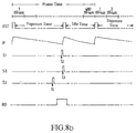
- the compensation can be made only to the portion caused by the ADC circuits between columns.
- the occurrence of the pulses at time t2 and t3 on signals S1, S2 in FIG. 8(b) involve the sampling of the actual image signal.
- the voltage at the output of CDS circuit 18 would then be converted to a digital value by ADC circuit 16 at time period after t 1d and before t2 shown in Figure 6(b), or after t 1 and before t 2 in Figure 7(b) and Figure 8(b). If the offset voltage for each comparator of ADC circuit as well as CDS circuit for each column within array deviates from that of others, it will be expected that the digital value output from ADC circuit would be different among columns under the same Vref signal.
- the binary complement to the digital value obtained for one ADC circuit during an initialization period is used to initialize the counter within the corresponding ADC 16 before the actual image value conversion for each row line within a frame time slot is performed. That is, each initial value of the ADC's counters with respect to respective columns are used to minimize the offset caused by the ADC and the CDS circuits between columns.
- the invention may be further realized by the following elaboration of exemplary operation results.
- the maximum difference of the signal input to the CDS circuit may be 3 volts and therefore outputs an analog signal of substantial 3.5 volts.
- the minimum difference of the signal input to the CDS circuit may be 0.5 volts and therefore outputs an analog signal of substantial 0 volts. Therefore, the dynamic range of output of the A/D converter 16 goes from 0 volts to 3.5 volts when taking into account the Vsh.
- the present invention provides an initialization period during which an autocalibration of the counter within the A/D converter is performed to offset all non-uniformity among different pixel columns within the array. For each image frame time, the initialization of the counter is performed once before the read operation of the first row of the frame by presetting the input of CDS 18 or A/D converter 16 of each column line to a reference voltage Vref.
- An A/D convert operation is then performed to generate the corresponding digital output data for each column.
- the result of A/D conversion operation for three column lines X, Y, and Z respectively are those shown in items (4), (5), and (6).
- the present invention uses the data in items (4), (5), and (6) to obtain the required offset values by inverting the binary data of (4), (5), and (6) to their binary complement, respectively, as listed below in items (7), (8), and (9).
- Column X: 00000000 0(decimal)
- Column Y: 00100101 37(decimal)
- Column Z: 01001001 73(decimal)
- the above binary complementary data are respectively used to initialize the respective counter within each ADC circuit 16 corresponding to column lines X, Y and Z.
- the initial value of the counter within each ADC circuit 16 corresponding to columns line X, line Y, line Z is 0, 37 and 73 respectively.
- an initialization circuit shown in Fig. 10 is connected to the counter within the A/D converter and the output of the initialization circuit is used to initialize the counter within the A/D converter according to the invention during the initialization period.
- the latch-enabling signal is used to latch the output signal from counter into the latch of the initialization circuit.
- the SCTR signal enables the output (IS0, IS1,....IS7) from the latch to preload the counter as recited above.
- the resulting A/D output for column line X will be 0 + 255, i.e. 255, by the invention.
- the resulting A/D output for column line Y will be 37 + 218, i.e. 255, by the invention.
- the resulting A/D output for column line Z will be 73 + 182 , i.e. 255, by the invention.
- the respective A/D output for the column line X, line Y, line Z without the invention will be those shown in list items (1), (2) and (3). Contractingly, with the implementation of the invention, the respective A/D outputs for the column line X, line Y, line Z are all equal to 255 and the uniformity of all columns is achieved as expected.
- the resulting A/D output for column line X will be 0 + 73, i.e. 73, by the invention.
- the resulting A/D output for column line Y will be 37 +36 , i.e. 73, by the invention.
- the resulting A/D output for column line Z will be 73+ 0, i.e. 73, by the invention.
- the respective A/D output without the invention, will be those shown in list items (10), (11) and (12). Contrastingly, with the implementation of the invention, the respective A/D outputs are all equal to 73 and the uniformity of all columns is achieved as expected.
- bits of ADC counter can increase beyond 8 bits to meet requirement.
- Types of ADC other than that shown in FIG. 3 are available and may be used but still achieve the objective of the invention without departing from the spirit of the invention.
- the initialization value may be obtained by complementing the output of each ADC during the initialization period for each frame.
- the initialization values obtained then are stored in a data latch circuit.
- these values then are respectively added to each output of the ADC by an additional adder circuit to offset the non-uniformity among the columns.
Landscapes
- Engineering & Computer Science (AREA)
- Multimedia (AREA)
- Signal Processing (AREA)
- Theoretical Computer Science (AREA)
- Transforming Light Signals Into Electric Signals (AREA)
- Facsimile Heads (AREA)
Applications Claiming Priority (2)
| Application Number | Priority Date | Filing Date | Title |
|---|---|---|---|
| US09/103,959 US6583817B1 (en) | 1998-06-24 | 1998-06-24 | Autocalibration of the A/D converter within the CMOS type image sensor |
| US103959 | 2005-04-12 |
Publications (2)
| Publication Number | Publication Date |
|---|---|
| EP0967729A2 true EP0967729A2 (de) | 1999-12-29 |
| EP0967729A3 EP0967729A3 (de) | 2004-03-17 |
Family
ID=22297921
Family Applications (1)
| Application Number | Title | Priority Date | Filing Date |
|---|---|---|---|
| EP99111919A Withdrawn EP0967729A3 (de) | 1998-06-24 | 1999-06-22 | Selbstkalibrierung eines AD-Wandlers in einem Bildsensor des CMOS-Typs |
Country Status (4)
| Country | Link |
|---|---|
| US (1) | US6583817B1 (de) |
| EP (1) | EP0967729A3 (de) |
| KR (1) | KR100616074B1 (de) |
| TW (1) | TW444404B (de) |
Cited By (4)
| Publication number | Priority date | Publication date | Assignee | Title |
|---|---|---|---|---|
| DE10226458B3 (de) * | 2002-06-13 | 2004-01-22 | Deutsches Zentrum für Luft- und Raumfahrt e.V. | Verfahren und Vorrichtung zur Linearisierung von photosensitiven Sensoren |
| EP1137262A3 (de) * | 2000-02-02 | 2004-10-20 | Taiwan Advanced Sensors Corporation | Zeilensprungbildelementgestaltung für CMOS Bildsensoren mit hoher Empfindlichkeit |
| US7646410B2 (en) | 2005-03-09 | 2010-01-12 | Samsung Electronics Co., Ltd. | Solid state image sensing device and method for subsampling using inter-column analog domain signal summation |
| EP2693740A3 (de) * | 2012-07-31 | 2017-07-26 | Canon Kabushiki Kaisha | Bildaufnahmesensor - Ansteuerungsvorrichtung, Verfahren und Strahlenabbildungsvorrichtung |
Families Citing this family (21)
| Publication number | Priority date | Publication date | Assignee | Title |
|---|---|---|---|---|
| US7139025B1 (en) * | 1998-10-29 | 2006-11-21 | Micron Technology, Inc. | Active pixel sensor with mixed analog and digital signal integration |
| US6965407B2 (en) * | 2001-03-26 | 2005-11-15 | Silicon Video, Inc. | Image sensor ADC and CDS per column |
| JP4022862B2 (ja) * | 2002-06-11 | 2007-12-19 | ソニー株式会社 | 固体撮像装置及びその制御方法 |
| US7046284B2 (en) * | 2003-09-30 | 2006-05-16 | Innovative Technology Licensing Llc | CMOS imaging system with low fixed pattern noise |
| DE60333757D1 (de) * | 2003-11-04 | 2010-09-23 | St Microelectronics Res & Dev | Verbesserungen in oder in Bezug auf Bildsensoren |
| US7446806B2 (en) * | 2003-12-19 | 2008-11-04 | Symbol Technologies, Inc. | Single chip, noise-resistant, one-dimensional, CMOS sensor for target imaging |
| GB2411060B (en) * | 2004-02-12 | 2007-10-24 | Micron Technology Inc | Low power comparator |
| JP4289206B2 (ja) * | 2004-04-26 | 2009-07-01 | ソニー株式会社 | カウンタ回路 |
| JP4157083B2 (ja) * | 2004-09-09 | 2008-09-24 | マイクロン テクノロジー,インコーポレイテッド | オンチップ半列並列パイプラインアナログ‐デジタル変換器を具えるイメージセンサ |
| KR100674966B1 (ko) * | 2005-03-23 | 2007-01-26 | 삼성전자주식회사 | 동작중에도 아날로그 디지털 변환기의 특성을 검사할 수있는 이미지 촬상용 반도체 장치 |
| KR100737915B1 (ko) * | 2005-12-16 | 2007-07-10 | 삼성전자주식회사 | 이미지 센서 그리고 그것을 위한 테스트 시스템 및 테스트방법 |
| US7242332B1 (en) * | 2006-05-04 | 2007-07-10 | Micron Technology, Inc. | Column-parallel sigma-delta analog-to-digital conversion with gain and offset control |
| TWI399088B (zh) * | 2007-10-12 | 2013-06-11 | Sony Corp | 資料處理器,固態成像裝置,成像裝置,及電子設備 |
| US7884865B2 (en) * | 2007-12-10 | 2011-02-08 | Intel Corporation | High speed noise detection and reduction in active pixel sensor arrays |
| JP5269456B2 (ja) * | 2008-03-26 | 2013-08-21 | 株式会社東芝 | イメージセンサおよびその駆動方法 |
| GB0806427D0 (en) * | 2008-04-09 | 2008-05-14 | Cmosis Nv | Parallel analog-to-digital conversion in pixel arrays |
| US8184184B2 (en) * | 2008-12-08 | 2012-05-22 | Omnivision Technologies, Inc. | Analog multiplexer configured to reduce kickback perturbation in image sensor readout |
| US8300126B2 (en) * | 2008-12-15 | 2012-10-30 | Altasens, Inc. | Staggered reset in CMOS digital sensor device |
| US8446309B2 (en) * | 2009-02-19 | 2013-05-21 | Cmosis Nv | Analog-to-digital conversion in pixel arrays |
| US9200956B2 (en) * | 2010-06-27 | 2015-12-01 | Sri International | Readout transistor circuits for CMOS imagers |
| TWI645707B (zh) * | 2013-10-21 | 2018-12-21 | 索尼半導體解決方案公司 | Solid-state imaging device and electronic device |
Family Cites Families (11)
| Publication number | Priority date | Publication date | Assignee | Title |
|---|---|---|---|---|
| US3445839A (en) * | 1965-01-14 | 1969-05-20 | American Standard Inc | Drift correction |
| US3849775A (en) * | 1972-10-24 | 1974-11-19 | Westinghouse Electric Corp | Ac analog to digital converter |
| GB1397288A (en) * | 1972-12-05 | 1975-06-11 | Comark Data Group | Analogue to digital converters |
| GB1564179A (en) * | 1976-06-11 | 1980-04-02 | Japan Atomic Energy Res Inst | Method of analogue-to-digital conversion |
| US5053770A (en) * | 1990-05-18 | 1991-10-01 | Analogic Corporation | Digital autozero circuit operable in a plurality of modes with separate storage for offset corrections for each mode |
| KR940008796B1 (ko) * | 1991-09-25 | 1994-09-26 | 삼성전자 주식회사 | 화상신호처리 방법 및 회로 |
| JPH0767152B2 (ja) * | 1993-03-25 | 1995-07-19 | 日本電気株式会社 | イメージセンサとその駆動方法 |
| US5949483A (en) * | 1994-01-28 | 1999-09-07 | California Institute Of Technology | Active pixel sensor array with multiresolution readout |
| JPH07264073A (ja) * | 1994-03-18 | 1995-10-13 | Fuji Electric Co Ltd | A/d変換回路 |
| US6115066A (en) * | 1997-06-12 | 2000-09-05 | International Business Machines Corporation | Image sensor with direct digital correlated sampling |
| US5877715A (en) * | 1997-06-12 | 1999-03-02 | International Business Machines Corporation | Correlated double sampling with up/down counter |
-
1998
- 1998-06-24 US US09/103,959 patent/US6583817B1/en not_active Expired - Lifetime
-
1999
- 1999-06-14 TW TW088109911A patent/TW444404B/zh not_active IP Right Cessation
- 1999-06-22 EP EP99111919A patent/EP0967729A3/de not_active Withdrawn
- 1999-06-24 KR KR1019990024071A patent/KR100616074B1/ko not_active Expired - Fee Related
Cited By (6)
| Publication number | Priority date | Publication date | Assignee | Title |
|---|---|---|---|---|
| EP1137262A3 (de) * | 2000-02-02 | 2004-10-20 | Taiwan Advanced Sensors Corporation | Zeilensprungbildelementgestaltung für CMOS Bildsensoren mit hoher Empfindlichkeit |
| DE10226458B3 (de) * | 2002-06-13 | 2004-01-22 | Deutsches Zentrum für Luft- und Raumfahrt e.V. | Verfahren und Vorrichtung zur Linearisierung von photosensitiven Sensoren |
| US7646410B2 (en) | 2005-03-09 | 2010-01-12 | Samsung Electronics Co., Ltd. | Solid state image sensing device and method for subsampling using inter-column analog domain signal summation |
| EP2693740A3 (de) * | 2012-07-31 | 2017-07-26 | Canon Kabushiki Kaisha | Bildaufnahmesensor - Ansteuerungsvorrichtung, Verfahren und Strahlenabbildungsvorrichtung |
| US9756267B2 (en) | 2012-07-31 | 2017-09-05 | Canon Kabushiki Kaisha | Image sensor driving apparatus, method and radiation imaging apparatus |
| US10148898B2 (en) | 2012-07-31 | 2018-12-04 | Canon Kabushiki Kaisha | Image sensor driving apparatus, method and radiation imaging apparatus |
Also Published As
| Publication number | Publication date |
|---|---|
| TW444404B (en) | 2001-07-01 |
| EP0967729A3 (de) | 2004-03-17 |
| KR20000006432A (ko) | 2000-01-25 |
| KR100616074B1 (ko) | 2006-08-25 |
| US6583817B1 (en) | 2003-06-24 |
Similar Documents
| Publication | Publication Date | Title |
|---|---|---|
| US6583817B1 (en) | Autocalibration of the A/D converter within the CMOS type image sensor | |
| US10986296B2 (en) | Solid-state image pickup device and control method thereof | |
| Furuta et al. | A high-speed, high-sensitivity digital CMOS image sensor with a global shutter and 12-bit column-parallel cyclic A/D converters | |
| CN1980335B (zh) | 产生信号中噪声降低的信号的信号发生器和方法 | |
| TW550942B (en) | CMOS image sensor having chopper type comparator to perform analog correlated double sampling | |
| US7310452B2 (en) | Offset adjustment methods of signal converting circuits | |
| US8022856B2 (en) | Successive approximation type A/D converter, method of controlling successive approximation type A/D converter, solid-state imaging device, and imaging apparatus | |
| US6344877B1 (en) | Image sensor with dummy pixel or dummy pixel array | |
| US6965407B2 (en) | Image sensor ADC and CDS per column | |
| US5461425A (en) | CMOS image sensor with pixel level A/D conversion | |
| US8462243B2 (en) | Solid-state image sensing device, method for reading signal of solid-state image sensing device, and image pickup apparatus | |
| US6229133B1 (en) | Image sensing device with delayed phase frequency modulation | |
| US6525304B1 (en) | Circuitry for converting analog signals from pixel sensor to a digital and for storing the digital signal | |
| US7626618B2 (en) | Solid-state image pickup device, driving method for solid-state image pickup device and image pickup apparatus | |
| US20070216564A1 (en) | AD converter device, physical quantity distribution detecting unit and imaging apparatus | |
| TWI830030B (zh) | 具有數位像素儲存的增量影像感測器 | |
| CN100479488C (zh) | Cmos图像传感器 | |
| US7012557B2 (en) | Ramp modulation ADC for imagers | |
| JP2001036816A (ja) | Cmos型イメージセンサ内のa/d変換器の自動較正 | |
| EP4131939B1 (de) | Festkörperbildgebungsvorrichtung, verfahren zur ansteuerung einer festkörperbildgebungsvorrichtung und elektronische vorrichtung | |
| Chen et al. | Logarithmic CMOS image sensor through multi-resolution analog-to-digital conversion | |
| KR100737915B1 (ko) | 이미지 센서 그리고 그것을 위한 테스트 시스템 및 테스트방법 | |
| US20040263655A1 (en) | Image sensor with digital output and inherent pixel non-uniformity suppression | |
| US20250211243A1 (en) | Analog-to-digital converter and analog-to-digital converting method | |
| Guo et al. | Offset-free Column Buffer for CMOS image sensor |
Legal Events
| Date | Code | Title | Description |
|---|---|---|---|
| PUAI | Public reference made under article 153(3) epc to a published international application that has entered the european phase |
Free format text: ORIGINAL CODE: 0009012 |
|
| AK | Designated contracting states |
Kind code of ref document: A2 Designated state(s): AT BE CH CY DE DK ES FI FR GB GR IE IT LI LU MC NL PT SE |
|
| AX | Request for extension of the european patent |
Free format text: AL;LT;LV;MK;RO;SI |
|
| 17P | Request for examination filed |
Effective date: 20000615 |
|
| PUAL | Search report despatched |
Free format text: ORIGINAL CODE: 0009013 |
|
| AK | Designated contracting states |
Kind code of ref document: A3 Designated state(s): AT BE CH CY DE DK ES FI FR GB GR IE IT LI LU MC NL PT SE |
|
| AX | Request for extension of the european patent |
Extension state: AL LT LV MK RO SI |
|
| RIC1 | Information provided on ipc code assigned before grant |
Ipc: 7H 03M 1/10 B Ipc: 7H 03M 1/06 A |
|
| 17Q | First examination report despatched |
Effective date: 20040830 |
|
| AKX | Designation fees paid |
Designated state(s): BE CH DE FI FR GB IT LI NL |
|
| 17Q | First examination report despatched |
Effective date: 20040830 |
|
| GRAP | Despatch of communication of intention to grant a patent |
Free format text: ORIGINAL CODE: EPIDOSNIGR1 |
|
| STAA | Information on the status of an ep patent application or granted ep patent |
Free format text: STATUS: THE APPLICATION IS DEEMED TO BE WITHDRAWN |
|
| 18D | Application deemed to be withdrawn |
Effective date: 20071106 |