EP0967735A1 - Dispositif de filtrage applicable à un séparateur de signal ADSL - Google Patents
Dispositif de filtrage applicable à un séparateur de signal ADSL Download PDFInfo
- Publication number
- EP0967735A1 EP0967735A1 EP98401602A EP98401602A EP0967735A1 EP 0967735 A1 EP0967735 A1 EP 0967735A1 EP 98401602 A EP98401602 A EP 98401602A EP 98401602 A EP98401602 A EP 98401602A EP 0967735 A1 EP0967735 A1 EP 0967735A1
- Authority
- EP
- European Patent Office
- Prior art keywords
- filter
- transistor
- inductor
- line
- coupled
- Prior art date
- Legal status (The legal status is an assumption and is not a legal conclusion. Google has not performed a legal analysis and makes no representation as to the accuracy of the status listed.)
- Granted
Links
- 101150012579 ADSL gene Proteins 0.000 title abstract 4
- 102100020775 Adenylosuccinate lyase Human genes 0.000 title abstract 4
- 108700040193 Adenylosuccinate lyases Proteins 0.000 title abstract 4
- 230000005540 biological transmission Effects 0.000 claims abstract description 16
- 239000003990 capacitor Substances 0.000 claims description 6
- 230000001052 transient effect Effects 0.000 abstract description 8
- RYGMFSIKBFXOCR-UHFFFAOYSA-N Copper Chemical compound [Cu] RYGMFSIKBFXOCR-UHFFFAOYSA-N 0.000 abstract description 3
- 229910052802 copper Inorganic materials 0.000 abstract description 3
- 239000010949 copper Substances 0.000 abstract description 3
- 230000000694 effects Effects 0.000 description 3
- 230000011664 signaling Effects 0.000 description 2
- 230000002238 attenuated effect Effects 0.000 description 1
- 230000000295 complement effect Effects 0.000 description 1
- 239000013256 coordination polymer Substances 0.000 description 1
- 230000007423 decrease Effects 0.000 description 1
- 230000003247 decreasing effect Effects 0.000 description 1
- 230000008713 feedback mechanism Effects 0.000 description 1
- 239000000835 fiber Substances 0.000 description 1
- 238000001914 filtration Methods 0.000 description 1
Images

Classifications
-
- H—ELECTRICITY
- H03—ELECTRONIC CIRCUITRY
- H03H—IMPEDANCE NETWORKS, e.g. RESONANT CIRCUITS; RESONATORS
- H03H11/00—Networks using active elements
- H03H11/02—Multiple-port networks
- H03H11/04—Frequency selective two-port networks
- H03H11/12—Frequency selective two-port networks using amplifiers with feedback
- H03H11/1213—Frequency selective two-port networks using amplifiers with feedback using transistor amplifiers
Definitions
- the present invention relates to a filter arrangement to filter signals transmitted between a first filter port and a second filter port, said arrangement including filter means adapted to filter predetermined frequency components of said signals, and associated clamping means adapted to limit the transmission of unwanted signals between said first filter port and said second filter port.
- Such a filter arrangement is generally known in the art and is used to isolate the first filter port from the second filter port, and thereby the circuits, devices or apparatus connected to these ports.
- the signals may for instance be provided by a power supply or may be telecommunication signals whereby the filter arrangement is then used to separate different signals transmitted on a same telecommunication line but intended to different apparatus, as it is the case in a "party line" system where two telephone sets share a same transmission line, e.g. connected to the second filter port.
- many telecommunication modulation schemes use Frequency Division Multiplexing (FDM).
- FDM Frequency Division Multiplexing
- ADSL Asymmetric Digital Subscriber Line
- HDSL high frequency twisted pair of copper wires
- VADSL Plain Old Telephone Service
- a splitter is necessary to separate the high frequency ADSL signals, e.g. intended for an ADSL modem, from the lower frequency telephone signals, intended for a local telephone set.
- Such a splitter obviously includes a line filter arrangement.
- a high-pass filter is sitting in front of each modem, and a low-pass filter is sitting in front of each POTS interface.
- the line filter arrangement needs further also to be adapted for isolating the apparatus connected a local port, e.g. the first filter port, from the transmission line connected a line port, e.g. the second filter port, and this during severe changes in voltage/ current from one of the sides of the arrangement. This may for instance be the case of spikes on the signals and that have to be eliminated.
- splitters for ADSL and more particularly the filters included therein, are preferably based on passive filters. The main reason therefore is that they obviate the power provision issues and ensure continued functioning in the event of power failure. Passive filters are also able to cope more easily with large signals, both voltage and current, inherent in telephony signaling and powering.
- Passive filters have a linear behavior as they mostly use inductors and capacitors, whilst active filters use operational amplifiers and resistors.
- Such a linear approach makes the design relatively easy because the Laplace-transforms and network technology can be used.
- this easy design is only valid if everything remains linear in all conditions. In practice however, coils that saturate are no longer linear. This means that big, and thus relatively expensive, coils need to be provided to take care that they do not saturate.
- Transient signals are disturbances produced, e.g., by polarity reversal of the battery or by starting of the ringing signal at the side of the telecommunication exchange, and/ or by on-/ off- hook signals at the (user) side of the telephone set.
- large and expensive high (e.g. 7 th ) order filters are required as low-pass filters.
- Such transient and other over-current or over-voltage signals could, although not mentioned in the above known prior art, also be absorbed by clamping means such as Zener diodes adapted to eliminate voltage and/ or current spikes.
- clamping means such as Zener diodes adapted to eliminate voltage and/ or current spikes.
- An object of the present invention is to provide a filter arrangement of the above known type but which is adapted to filter transient signals in a more efficient way while being simpler and cheaper than the one known from the prior art.
- clamping means include active device means adapted to limit variations of predetermined parameters of said signals.
- the present invention is characterized in that said filter means includes at least one reactive device having a first end connected to said second filter port and a second end coupled to said first filter port via a main path of said active device means which further has a control terminal coupled to said first end of said reactive device.
- the present invention is further characterized in that said arrangement is a low-pass filter adapted to filter high frequency components of signals transmitted between said apparatus and said transmission line, in that said reactive device is an inductor, and in that said active device is a transistor.
- the present invention is further characterized in that said arrangement is a low-pass filter adapted to filter high frequency components of signals transmitted between said first filter port, which has a first and a second local terminal to which said apparatus is connected, and said second filter port, which has a first and a second line terminal to which said transmission line, that is a double-wired line, is connected, in that said filter means comprises a first inductor and a second inductor as reactive device and that said active device means comprise a first transistor and a second transistor, in that said first line terminal is connected to the first end of said first inductor, the second end of said first inductor being coupled to said first local terminal via the main path of said first transistor, and the control terminal of said first transistor being coupled to said first end of said first inductor, and in that said second line terminal is connected to the first end of said second inductor, the second end of said second inductor being coupled to said second local terminal via the main path of said second transistor, and the control terminal of said second transistor being coupled to said
- the arrangement is adapted to limit either positive and negative spikes of the transmitted signals, and it operates in a fully bi-directional way.
- said active device means further comprise a third transistor and a fourth transistor, that said first line terminal is connected to the first end of said first inductor via the main path of said third transistor, the control terminal of said third transistor being coupled to said second end of said first inductor, and that said second line terminal is connected to the first end of said second inductor via the main path of said fourth transistor, the control terminal of said fourth transistor being coupled to said second end of said second inductor.
- the present arrangement then shows balanced characteristics with respect to the devices connected thereto.
- the present invention is further also characterized in that said first and second line terminals are coupled via the series connected main paths of a pair of transistors of which the control terminals are connected to the first ends of said first and second inductors respectively.
- the currents limited by the filter means and their associated clamping means are then derived through this pair of transistors so that the present filter arrangement remains transparent for the device connected thereto.
- the filter arrangement of the present invention is particularly applicable to a splitter for an Asymmetric Digital Subscriber Line "ADSL" system as shown in Fig. 1.
- ADSL Asymmetric Digital Subscriber Line
- an ADSL system - or a similar system such as HDSL, VADSL, ... - is adapted to transmit voice and higher frequency signals over a classical copper twisted-pair telephone line TP.
- a splitter At each end of the twisted-pair transmission line TP is provided a splitter that separates the high frequency ADSL signals from the low frequency Plain Old Telephone Service POTS (or voice) signals.
- a splitter SP1 has a line port LI1 that connects an end of the transmission line TP both to a port LM1 of a local ADSL modem ADSLcp and to a local port LO1 of a user subscriber set POTS, whilst at the central office side CO another splitter SP2 has a line port LI2 that connects the other end of the transmission line TP both to a port LM2 of a central ADSL modem ADSLco and to a local port LO2 of a Public Switching Telecommunication Network PSTN.
- the splitter SP1 includes a high-pass filter HP1 that interconnects the ports LI1 and LM1, and a low-pass filter LP1 that interconnects the pods LI1 and LO1.
- the splitter SP2 includes a high-pass filter HP2 that interconnects the pods LI2 and LM2, and a low-pass filter LP2 that interconnects the pods LI2 and LO2.
- the present invention concerns an improved version of the low-pass filter LP1 or LP2, hereafter more generally called LP as shown at Fig. 2.
- This line filter arrangement LP is located between a first filter pod LO and a second filter pod LI, which respectively correspond to the above local pods LO1/LO2 and line ports LI1/LI2.
- the purpose of the filter LP is to isolate its two sides during severe changes in voltage/ current at one of these sides. As will be explained below, this is done by limiting or clamping the current variation dI/dt, where I is the current flowing through the filter.
- I is the current flowing through the filter.
- practical tests show that the latter provide slightly less efficient results.
- the pod LI of the filter LP has two line terminals LIa and LIb, whilst the port LO has two local terminals LOa and LOb.
- the line terminal LIa is connected to a first end of an inductor or coil L1 of which the second end is coupled to the local terminal LOa via the source-to-drain s-d (or main) path of a first FET transistor T1.
- the line terminal LIa, and thus the first end of the coil L1 is further also connected to the gate g or control terminal of the transistor T1.
- the voltage over the coil L1 is proportional to the variation dI/dt of the current I flowing therethrough. This voltage appears as gate-source voltage Vgs across the transistor T1 and thus determines what resistance the transistor T1 shows between its drain d and source s.
- dI/dt is small.
- the induced Vgs is therefore also small and, since the transistor T1 is of the depletion type, the resistance of its main path, i.e. between d and s, is small (about 3 Ohm) and will not change significantly.
- the transistor T1 can then just be seen as an inter-connection and the filter operates as a normal classical inductance filter.
- the above described filter arrangement LP including the inductor L1 and the transistor T1 between the filter ports LI and LO is sufficient to limit or clamp current variations in the one direction between these ports.
- the series connection of a second coil L2 and second transistor T2, arranged in a same way and respectively similar to L1 and T1 needs to be provided between the line terminal LIb and the local terminal LOb.
- the coils L1 and L2 are then magnetically coupled as shown in Fig. 2.
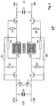
- the Fig. 3 shows a more practical implementation LP' of the filter arrangement LP.
- the filter LP' includes a third transistor T3 of which the main path connects the line terminal LIa to the first end of the coil L1, and a fourth transistor T4 of which the main path connects the line terminal LIb to the first end of the coil L2.
- the arrangement LP' then has balanced characteristics with respect to the devices connected thereto and the negative effect of possible common-mode signals are so eliminated.
- the gate or control terminals of the transistors T1, T2, T3 and T4 are connected to the opposite end of their associated coil via a resistor R1, R2, R3 and R4 respectively.
- a 7 th order low-pass filter is generally needed to filter-out the transients of the signals. It has however been proved that by limiting the variation dI/dt of the current I as by the present arrangement, the filter may be reduced to a 3 rd order filter while providing the same results.
- Such a 3 rd order filter is obtained by inserting a capacitor C1 between the line terminals LIa and LIb and a second capacitor C2 between the local terminals LOa and LOb.
- a 2 nd order filter should also be acceptable but then with less efficient results.
- the filter LP' is further protected against over-current and over-voltage by means of Zener diodes Z1, Z2, Z3 and Z4 connected between the gate and the source electrodes of the transistors T1, T2, T3 and T4.
- a pair of series connected transistors T5 and T6 is provided between the local terminals LOa and LOb.
- the gate or control terminal of T5 is connected to the gate of T1, whilst the gate of T6 is connected to that of T2.
- the transistors T5 and T6 are of the enhanced type. These transistors operate in a complementary way with respect to the transistors T1 to T4. In other words, when the current flow through the transistors T1-T4 decreases, the current flow through the transistors T5-T6 increases. It can be seen as the currents limited by T1-T4 are derived towards T5-T6, and that the current clamping operation is transparent for the devices connected to the present filter arrangement.
- a high-pass filter arrangement may also be designed on the same principle, mainly by replacing the inductors by capacitors.
Landscapes
- Filters And Equalizers (AREA)
- Networks Using Active Elements (AREA)
- Cable Transmission Systems, Equalization Of Radio And Reduction Of Echo (AREA)
Priority Applications (11)
| Application Number | Priority Date | Filing Date | Title |
|---|---|---|---|
| ES98401602T ES2271983T3 (es) | 1998-06-26 | 1998-06-26 | Disposicion de filtro aplicable a separadores de señal adsl. |
| DE69836263T DE69836263T2 (de) | 1998-06-26 | 1998-06-26 | Filteranordnung anwendbar auf ADSL-teiler |
| EP98401602A EP0967735B1 (fr) | 1998-06-26 | 1998-06-26 | Dispositif de filtrage applicable à un séparateur de signal ADSL |
| TW088108995A TW416204B (en) | 1998-06-26 | 1999-05-31 | Filter arrangement applicable to ADSL splitters |
| IL13025099A IL130250A0 (en) | 1998-06-26 | 1999-06-02 | Filter arrangement applicable to ADSL splitters |
| SG1999002840A SG74148A1 (en) | 1998-06-26 | 1999-06-05 | Filter arrangement applicable to adsl splitters |
| US09/326,544 US6628783B1 (en) | 1998-06-26 | 1999-06-07 | Filter arrangement applicable to ADSL splitters |
| JP16562699A JP4445063B2 (ja) | 1998-06-26 | 1999-06-11 | Adslスプリッタに適用可能なフィルタ構成 |
| CA002275007A CA2275007A1 (fr) | 1998-06-26 | 1999-06-15 | Dispositif-filtreur pouvant s'appliquer a des diviseurs de lnpa |
| AU36797/99A AU754589B2 (en) | 1998-06-26 | 1999-06-25 | Filter arrangement applicable to ADSL splitters |
| CN99111076A CN1132330C (zh) | 1998-06-26 | 1999-06-25 | 可应用于adsl分路器的滤波器配置 |
Applications Claiming Priority (1)
| Application Number | Priority Date | Filing Date | Title |
|---|---|---|---|
| EP98401602A EP0967735B1 (fr) | 1998-06-26 | 1998-06-26 | Dispositif de filtrage applicable à un séparateur de signal ADSL |
Publications (2)
| Publication Number | Publication Date |
|---|---|
| EP0967735A1 true EP0967735A1 (fr) | 1999-12-29 |
| EP0967735B1 EP0967735B1 (fr) | 2006-10-25 |
Family
ID=8235416
Family Applications (1)
| Application Number | Title | Priority Date | Filing Date |
|---|---|---|---|
| EP98401602A Expired - Lifetime EP0967735B1 (fr) | 1998-06-26 | 1998-06-26 | Dispositif de filtrage applicable à un séparateur de signal ADSL |
Country Status (11)
| Country | Link |
|---|---|
| US (1) | US6628783B1 (fr) |
| EP (1) | EP0967735B1 (fr) |
| JP (1) | JP4445063B2 (fr) |
| CN (1) | CN1132330C (fr) |
| AU (1) | AU754589B2 (fr) |
| CA (1) | CA2275007A1 (fr) |
| DE (1) | DE69836263T2 (fr) |
| ES (1) | ES2271983T3 (fr) |
| IL (1) | IL130250A0 (fr) |
| SG (1) | SG74148A1 (fr) |
| TW (1) | TW416204B (fr) |
Cited By (8)
| Publication number | Priority date | Publication date | Assignee | Title |
|---|---|---|---|---|
| FR2834592A1 (fr) * | 2002-01-10 | 2003-07-11 | Europe Adsl Lab | Dispositif de filtrage passe-bas destine au decouplage des voies xdsl |
| FR2848041A1 (fr) * | 2002-11-29 | 2004-06-04 | Europe Adsl Leacom Fastnet Lab | Filtre passe bas avec asic destine aux lignes telephoniques adaptees a la transmission adsl |
| EP1117217A3 (fr) * | 2000-01-14 | 2004-06-09 | Corning Cable Systems LLC | Un dispositif d'inductance sensible à la fréquence pour la conception de diviseurs de téléphonie traditionelle |
| US6856192B2 (en) | 2001-10-10 | 2005-02-15 | Yamaha Corporation | Class-D amplifier of BTL output type using filter coil and low-pass filter |
| US7333606B1 (en) | 2000-04-13 | 2008-02-19 | Adc Telecommunications, Inc. | Splitter architecture for a telecommunications system |
| CN100449941C (zh) * | 2002-04-05 | 2009-01-07 | 欧洲Adsl实验室 | 低频滤波装置 |
| EP2066103A1 (fr) * | 2007-11-30 | 2009-06-03 | Alcatel Lucent | Séparateur xdsl à indépendance commutable |
| EP2469675A4 (fr) * | 2010-02-09 | 2013-03-20 | Huawei Tech Co Ltd | Circuit de protection de ligne d'abonné numérique (« digital subscriber line » ou dsl) |
Families Citing this family (9)
| Publication number | Priority date | Publication date | Assignee | Title |
|---|---|---|---|---|
| US6188750B1 (en) | 1998-11-19 | 2001-02-13 | Excelsus Technologies, Inc. | Impedance blocking filter circuit |
| US6886181B1 (en) * | 2000-07-07 | 2005-04-26 | Critical Telecom Corp. | Extended distribution of ADSL signals |
| US20020141570A1 (en) * | 2001-04-03 | 2002-10-03 | Ting Sun | Low-pass filter usable with caller ID device |
| CA2358379A1 (fr) * | 2001-10-05 | 2003-04-05 | Elysium Broadband Inc. | Methode et systeme pour empecher les pertes de signal dans les prises de pontage a impedance non adaptee |
| DE10151949B4 (de) * | 2001-10-22 | 2011-08-11 | Lantiq Deutschland GmbH, 85579 | Splitter-Schaltungsanordnung |
| DE60311845D1 (de) * | 2003-12-22 | 2007-03-29 | St Microelectronics Srl | Aktive Impedanzsyntheseschaltung, beispielsweise für XDSL-Teiler |
| US9077818B2 (en) * | 2005-04-13 | 2015-07-07 | Alcatel Lucent | Remotely migrating from a first service to a second service |
| US8027461B1 (en) * | 2007-10-11 | 2011-09-27 | Adtran, Inc. | Systems and methods for splitting telecommunication signals with reduced noise |
| CN110830025A (zh) * | 2019-11-27 | 2020-02-21 | 珠海复旦创新研究院 | 一种支持多频段工作的互感耦合器 |
Citations (1)
| Publication number | Priority date | Publication date | Assignee | Title |
|---|---|---|---|---|
| EP0251986A2 (fr) * | 1986-07-02 | 1988-01-07 | Eci Telecom Ltd. | Appareil pour usage multiple d'une ligne téléphonique avec générateur de courant de sonnerie |
Family Cites Families (4)
| Publication number | Priority date | Publication date | Assignee | Title |
|---|---|---|---|---|
| US4268807A (en) * | 1978-07-13 | 1981-05-19 | Spence Lewis C | Band-pass filter and gain stage |
| ES244069Y (es) * | 1979-06-21 | 1980-04-01 | Circuito detector de corriente. | |
| DE3538088C2 (de) * | 1985-10-25 | 1993-11-11 | Siemens Ag | Schaltungsanordnung für einen Überspannungsschutz in elektronischen Fernsprechstationen |
| US6144735A (en) * | 1998-03-12 | 2000-11-07 | Westell Technologies, Inc. | Filters for a digital subscriber line system for voice communication over a telephone line |
-
1998
- 1998-06-26 DE DE69836263T patent/DE69836263T2/de not_active Expired - Lifetime
- 1998-06-26 ES ES98401602T patent/ES2271983T3/es not_active Expired - Lifetime
- 1998-06-26 EP EP98401602A patent/EP0967735B1/fr not_active Expired - Lifetime
-
1999
- 1999-05-31 TW TW088108995A patent/TW416204B/zh not_active IP Right Cessation
- 1999-06-02 IL IL13025099A patent/IL130250A0/xx unknown
- 1999-06-05 SG SG1999002840A patent/SG74148A1/en unknown
- 1999-06-07 US US09/326,544 patent/US6628783B1/en not_active Expired - Fee Related
- 1999-06-11 JP JP16562699A patent/JP4445063B2/ja not_active Expired - Fee Related
- 1999-06-15 CA CA002275007A patent/CA2275007A1/fr not_active Abandoned
- 1999-06-25 CN CN99111076A patent/CN1132330C/zh not_active Expired - Fee Related
- 1999-06-25 AU AU36797/99A patent/AU754589B2/en not_active Ceased
Patent Citations (1)
| Publication number | Priority date | Publication date | Assignee | Title |
|---|---|---|---|---|
| EP0251986A2 (fr) * | 1986-07-02 | 1988-01-07 | Eci Telecom Ltd. | Appareil pour usage multiple d'une ligne téléphonique avec générateur de courant de sonnerie |
Non-Patent Citations (1)
| Title |
|---|
| COOK J ET AL: "ADSL AND VADSL SPLITTER DESIGN AND TELEPHONY PERFORMANCE", IEEE JOURNAL ON SELECTED AREAS IN COMMUNICATIONS, vol. 13, no. 9, 1 December 1995 (1995-12-01), pages 1634 - 1642, XP000543160 * |
Cited By (11)
| Publication number | Priority date | Publication date | Assignee | Title |
|---|---|---|---|---|
| EP1117217A3 (fr) * | 2000-01-14 | 2004-06-09 | Corning Cable Systems LLC | Un dispositif d'inductance sensible à la fréquence pour la conception de diviseurs de téléphonie traditionelle |
| US7333606B1 (en) | 2000-04-13 | 2008-02-19 | Adc Telecommunications, Inc. | Splitter architecture for a telecommunications system |
| US6856192B2 (en) | 2001-10-10 | 2005-02-15 | Yamaha Corporation | Class-D amplifier of BTL output type using filter coil and low-pass filter |
| FR2834592A1 (fr) * | 2002-01-10 | 2003-07-11 | Europe Adsl Lab | Dispositif de filtrage passe-bas destine au decouplage des voies xdsl |
| WO2003061121A1 (fr) * | 2002-01-10 | 2003-07-24 | Laboratoire Europeen Adsl Leacom Fastnet | Dispositif de filtrage passe-bas destiné au découplage des voies xdsl |
| CN100449941C (zh) * | 2002-04-05 | 2009-01-07 | 欧洲Adsl实验室 | 低频滤波装置 |
| FR2848041A1 (fr) * | 2002-11-29 | 2004-06-04 | Europe Adsl Leacom Fastnet Lab | Filtre passe bas avec asic destine aux lignes telephoniques adaptees a la transmission adsl |
| WO2004051977A3 (fr) * | 2002-11-29 | 2004-08-05 | Europe Adsl Leacom Fastnet Lab | Filtre passe bas destine aux lignes telephoniques adaptees a la transmission adsl. |
| EP2066103A1 (fr) * | 2007-11-30 | 2009-06-03 | Alcatel Lucent | Séparateur xdsl à indépendance commutable |
| EP2469675A4 (fr) * | 2010-02-09 | 2013-03-20 | Huawei Tech Co Ltd | Circuit de protection de ligne d'abonné numérique (« digital subscriber line » ou dsl) |
| US8625246B2 (en) | 2010-02-09 | 2014-01-07 | Huawei Technologies Co., Ltd. | DSL protection circuit |
Also Published As
| Publication number | Publication date |
|---|---|
| JP4445063B2 (ja) | 2010-04-07 |
| TW416204B (en) | 2000-12-21 |
| AU754589B2 (en) | 2002-11-21 |
| CN1252648A (zh) | 2000-05-10 |
| SG74148A1 (en) | 2000-07-18 |
| CN1132330C (zh) | 2003-12-24 |
| DE69836263T2 (de) | 2007-05-31 |
| AU3679799A (en) | 2000-01-13 |
| DE69836263D1 (de) | 2006-12-07 |
| CA2275007A1 (fr) | 1999-12-26 |
| US6628783B1 (en) | 2003-09-30 |
| EP0967735B1 (fr) | 2006-10-25 |
| JP2000151357A (ja) | 2000-05-30 |
| ES2271983T3 (es) | 2007-04-16 |
| IL130250A0 (en) | 2000-06-01 |
Similar Documents
| Publication | Publication Date | Title |
|---|---|---|
| EP0967735B1 (fr) | Dispositif de filtrage applicable à un séparateur de signal ADSL | |
| USRE40020E1 (en) | Impedance blocking filter circuit | |
| CA2314052C (fr) | Circuit de filtrage a blocage d'impedance | |
| JP3645263B2 (ja) | フィルタ作用 | |
| JP4482177B2 (ja) | フィルタ構成 | |
| KR20090069276A (ko) | xDSL 스플리터용 복수 차수의 저역 통과 필터 | |
| WO2000048314A1 (fr) | Multiplexage et demultiplexage de services bande etroite et bande large dans une connexion de transmission | |
| EP1248444A1 (fr) | Appareil téléphonique de test analogue possedant un filtre passe-bas et des resistances couplées avec les lignes de connection pour prévenir l'alteration des signaux de communication numériques | |
| US6757380B2 (en) | Impedance blocking filter circuit for digital subscriber line communication systems | |
| US8165283B2 (en) | Advanced ADSL splitter | |
| SE514378C2 (sv) | Aktiv impedansomvandlarkrets och splitter samt terminering av en tvinnad parledning | |
| AU2006100159A6 (en) | A filter | |
| CA2424855C (fr) | Filtre passe-bas en cascade pour ameliorer l'affaiblissement d'une bande xdsl, pour coupleur de telephone ordinaire | |
| HK1039847B (en) | Impedance blocking filter circuit | |
| US20040135651A1 (en) | Filter arragement | |
| AU2003201366A1 (en) | Variable response ADSL filter |
Legal Events
| Date | Code | Title | Description |
|---|---|---|---|
| PUAI | Public reference made under article 153(3) epc to a published international application that has entered the european phase |
Free format text: ORIGINAL CODE: 0009012 |
|
| AK | Designated contracting states |
Kind code of ref document: A1 Designated state(s): BE DE ES FR GB IT SE |
|
| AX | Request for extension of the european patent |
Free format text: AL;LT;LV;MK;RO;SI |
|
| 17P | Request for examination filed |
Effective date: 20000629 |
|
| AKX | Designation fees paid |
Free format text: BE DE ES FR GB IT SE |
|
| 17Q | First examination report despatched |
Effective date: 20040309 |
|
| GRAP | Despatch of communication of intention to grant a patent |
Free format text: ORIGINAL CODE: EPIDOSNIGR1 |
|
| GRAS | Grant fee paid |
Free format text: ORIGINAL CODE: EPIDOSNIGR3 |
|
| GRAA | (expected) grant |
Free format text: ORIGINAL CODE: 0009210 |
|
| AK | Designated contracting states |
Kind code of ref document: B1 Designated state(s): BE DE ES FR GB IT SE |
|
| PG25 | Lapsed in a contracting state [announced via postgrant information from national office to epo] |
Ref country code: BE Free format text: LAPSE BECAUSE OF FAILURE TO SUBMIT A TRANSLATION OF THE DESCRIPTION OR TO PAY THE FEE WITHIN THE PRESCRIBED TIME-LIMIT Effective date: 20061025 |
|
| REG | Reference to a national code |
Ref country code: GB Ref legal event code: FG4D |
|
| REF | Corresponds to: |
Ref document number: 69836263 Country of ref document: DE Date of ref document: 20061207 Kind code of ref document: P |
|
| PG25 | Lapsed in a contracting state [announced via postgrant information from national office to epo] |
Ref country code: SE Free format text: LAPSE BECAUSE OF FAILURE TO SUBMIT A TRANSLATION OF THE DESCRIPTION OR TO PAY THE FEE WITHIN THE PRESCRIBED TIME-LIMIT Effective date: 20070125 |
|
| REG | Reference to a national code |
Ref country code: ES Ref legal event code: FG2A Ref document number: 2271983 Country of ref document: ES Kind code of ref document: T3 |
|
| RAP2 | Party data changed (patent owner data changed or rights of a patent transferred) |
Owner name: ALCATEL LUCENT |
|
| ET | Fr: translation filed | ||
| PGFP | Annual fee paid to national office [announced via postgrant information from national office to epo] |
Ref country code: ES Payment date: 20070727 Year of fee payment: 10 |
|
| PLBE | No opposition filed within time limit |
Free format text: ORIGINAL CODE: 0009261 |
|
| STAA | Information on the status of an ep patent application or granted ep patent |
Free format text: STATUS: NO OPPOSITION FILED WITHIN TIME LIMIT |
|
| 26N | No opposition filed |
Effective date: 20070726 |
|
| REG | Reference to a national code |
Ref country code: ES Ref legal event code: FD2A Effective date: 20080627 |
|
| PG25 | Lapsed in a contracting state [announced via postgrant information from national office to epo] |
Ref country code: IT Free format text: LAPSE BECAUSE OF NON-PAYMENT OF DUE FEES Effective date: 20070626 |
|
| PG25 | Lapsed in a contracting state [announced via postgrant information from national office to epo] |
Ref country code: ES Free format text: LAPSE BECAUSE OF NON-PAYMENT OF DUE FEES Effective date: 20080627 |
|
| PGFP | Annual fee paid to national office [announced via postgrant information from national office to epo] |
Ref country code: GB Payment date: 20140618 Year of fee payment: 17 |
|
| REG | Reference to a national code |
Ref country code: FR Ref legal event code: GC Effective date: 20140717 |
|
| PGFP | Annual fee paid to national office [announced via postgrant information from national office to epo] |
Ref country code: DE Payment date: 20140619 Year of fee payment: 17 |
|
| PGFP | Annual fee paid to national office [announced via postgrant information from national office to epo] |
Ref country code: FR Payment date: 20140619 Year of fee payment: 17 |
|
| REG | Reference to a national code |
Ref country code: FR Ref legal event code: CA Effective date: 20150521 |
|
| REG | Reference to a national code |
Ref country code: FR Ref legal event code: CA Effective date: 20150521 |
|
| REG | Reference to a national code |
Ref country code: DE Ref legal event code: R119 Ref document number: 69836263 Country of ref document: DE |
|
| GBPC | Gb: european patent ceased through non-payment of renewal fee |
Effective date: 20150626 |
|
| REG | Reference to a national code |
Ref country code: FR Ref legal event code: ST Effective date: 20160229 |
|
| PG25 | Lapsed in a contracting state [announced via postgrant information from national office to epo] |
Ref country code: GB Free format text: LAPSE BECAUSE OF NON-PAYMENT OF DUE FEES Effective date: 20150626 Ref country code: DE Free format text: LAPSE BECAUSE OF NON-PAYMENT OF DUE FEES Effective date: 20160101 |
|
| PG25 | Lapsed in a contracting state [announced via postgrant information from national office to epo] |
Ref country code: FR Free format text: LAPSE BECAUSE OF NON-PAYMENT OF DUE FEES Effective date: 20150630 |