EP0969545A2 - Coupleur directionnel, dispositif d' antenne, et émetteur-récepteur - Google Patents
Coupleur directionnel, dispositif d' antenne, et émetteur-récepteur Download PDFInfo
- Publication number
- EP0969545A2 EP0969545A2 EP99112473A EP99112473A EP0969545A2 EP 0969545 A2 EP0969545 A2 EP 0969545A2 EP 99112473 A EP99112473 A EP 99112473A EP 99112473 A EP99112473 A EP 99112473A EP 0969545 A2 EP0969545 A2 EP 0969545A2
- Authority
- EP
- European Patent Office
- Prior art keywords
- dielectric
- guide
- directional coupler
- guides
- conductive plates
- Prior art date
- Legal status (The legal status is an assumption and is not a legal conclusion. Google has not performed a legal analysis and makes no representation as to the accuracy of the status listed.)
- Granted
Links
Images


Classifications
-
- H—ELECTRICITY
- H01—ELECTRIC ELEMENTS
- H01P—WAVEGUIDES; RESONATORS, LINES, OR OTHER DEVICES OF THE WAVEGUIDE TYPE
- H01P5/00—Coupling devices of the waveguide type
- H01P5/12—Coupling devices having more than two ports
- H01P5/16—Conjugate devices, i.e. devices having at least one port decoupled from one other port
- H01P5/18—Conjugate devices, i.e. devices having at least one port decoupled from one other port consisting of two coupled guides, e.g. directional couplers
- H01P5/188—Conjugate devices, i.e. devices having at least one port decoupled from one other port consisting of two coupled guides, e.g. directional couplers the guides being dielectric waveguides
Definitions
- the present invention relates to a directional coupler using a dielectric guide, and to an antenna device and a transceiver using the directional coupler.
- a dielectric guide comprising a dielectric strip provided between two conductive plates, is used as a guide for transmission in the milliwave band and the like.
- a directional coupler is used in a portion where electrical power is split between two dielectric guides.
- a conventional directional coupler using dielectric guides comprises two dielectric strips, having a linear portion and a curved portion, which are provided at a predetermined distance apart between two conductive plates. The dielectric strips are arranged close together and the dielectric guides are coupled at this closely arranged portion.
- a milliwave radar is an example of the milliwave circuit using dielectric guides described above.
- An antenna device used in a milliwave radar comprises a dielectric lens and a primary emitter provided at the focal point of the dielectric lens.
- One conceivable solution is to provide an antenna device, combining a primary emitter and a dielectric lens, in which the direction of the beam is tilted by changing the position of the primary emitter.
- the configuration should be arranged so that the dielectric guide connecting to the primary emitter and the other dielectric guide connecting to the circuit can be relatively displaced while remaining coupled with low loss.
- the configuration of the directional coupler using dielectric guides described above need only be arranged so that two dielectric guides can be relatively displaced.
- the separated positions (separated faces) of the two dielectric guides of the directional coupler are parallel to the two dielectric strips provided closely together.
- the end faces of the conductive plates on either side of the dielectric strips are provided parallel to the direction of propagation of the electromagnetic waves of the two dielectric guides, and consequently the path of the current flowing through the conductive plates is broken at the end face portions of the conductive plates, causing reflection.
- problems such as the creation of unwanted modes other than the propagation mode, increased loss, or an inability to obtain desired characteristics of the directional coupler, etc.
- the directional coupler can be used when forming a single device incorporating circuit modules using dielectric guides, to couple the dielectric guides between the circuit modules.
- the path of the current flowing through the conductive plates is broken between the circuit modules, causing reflection.
- a bend must be provided in dielectric guide portions joined to the directional coupler.
- the radius of curvature of the bend must be large. As a result, the overall size of the device is increased, and when it is used to form an antenna device, the moving portion cannot be made light, making it difficult to deflect the beam quickly.
- the coupling portion when the space between opposing faces of the two conductive plates clasping the dielectric strip is made narrow, although the radius of curvature of the bend can be set freely as long as dielectric guides transmitting only in the LSM01 mode as used, the coupling portion must be made long in order to obtain adequate coupling, inevitably increasing the overall size of the device and making it difficult to lighten the moving portion. If the space between the dielectric strips in the coupling portion is extremely narrow, strong coupling can be obtained, but the characteristics of the directional coupler will greatly depend on the precision of the positioning of the two separated dielectric guides.
- It is another object of the present invention enable the directional coupler and a device using the directional coupler to be easily miniturized, to enable the mass of the moving portion to be reduced, and to enable the direction of the beam to be deflected quickly.
- the directional coupler of the present invention comprises first and second dielectric guides, each comprising a dielectric strip provided between two conductive plates, arranged with the end faces of the conductive plates touching or not touching, and the dielectric strips of the first and second dielectric guides are provided substantially parallel to each other in the vicinity of the end faces of the conductive plates, so that the first and second dielectric guides are structurally separate. Furthermore, a groove is provided in an end face of the conductive plates of one of the first and second dielectric guide, the groove having a short-circuiting face in a position at a distance from the electrode faces of approximately an integral multiple of half the wavelength of a propagated wave.
- the electrode faces in the portion where the end faces of the conductive plates of the first and second dielectric guides are aligned function as an equivalently continuous portion. Therefore, although the two dielectric guides are separated by the conductive plate portions, there is almost no loss in this space. Furthermore, since there is almost no reflection, no spurious modes are caused by reflection.
- a position at a distance from the electrode face of approximately an integral multiple of half the wavelength of a plane wave, which travels in a direction such that it has a wave-number vector component equal to a phase constant of a transmitted wave propagating through the dielectric guides, in the direction of a transmitted wave propagating through the dielectric guides, is a short-circuiting face.
- the present invention further comprises a first type of nonradiative dielectric guide comprising the approximately parallel dielectric strip portions and the electrode faces, and a second type of nonradiative dielectric guide, wherein the space between the electrode faces other than those of the approximately parallel dielectric strip portions is narrower than the height of the approximately parallel dielectric strip portions, and comprising a dielectric strip portion other than the approximately parallel dielectric strip portions and the electrode faces, and transmitting in a single LSM01 mode.
- a guide conversion portion is provided between the first and second types of nonradiative dielectric guide. Consequently, coupling can easily be achieved in the first type of nonradiative dielectric guide portion, without increasing the length of the parallel dielectric strip portions or greatly narrowing the space between them.
- the second type of nonradiative dielectric guide portion there is no conversion to the LSE mode even when a bend with a short radius of curvature is provided, thereby enabling the entire device to be miniturized without increasing transmission loss.
- a primary emitter is coupled to a first dielectric guide of the above directional coupler, and a dielectric lens is secured approximately at the focal point of the primary emitter.
- the directional coupler When the directional coupler is arranged so that the amount of coupling between the first dielectric guide and the second dielectric guide of the directional coupler is approximately 0 dB, transmission signals and received signals can be transmitted most efficiently between the moving portion and the fixed portion, increasing the efficiency of the antenna.
- a transmission signal is sent from a transmitter to the second dielectric guide, and input/output ports of a circulator for sending a received signal from the second dielectric guide to a receiver are connected to the second dielectric guide.
- the present invention comprises a transceiver wherein a transmitter is connected to an input port of the circulator, and a receiver is connected to an output port of the circulator.
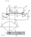
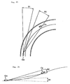
- FIGS. 1A and 1B show the relation between the configuration of a directional coupler and a primary emitter and a dielectric lens.
- FIG. 1A is a top view of the state when the upper conductive plate is removed
- FIG. 1B is a cross-sectional view through the primary emitter portion.
- a moving portion 31 can be displaced with respect to a fixed portion 32 in the direction indicated by the arrows.
- numeral 14 represents a lower conductive plate and numeral 11 represent a dielectric strip.
- the dielectric strip 11 is provided between an upper conductive plate and the lower conductive plate 14, thereby forming a first nonradiative dielectric guide (hereinafter "NRD guide").
- NRD guide first nonradiative dielectric guide
- numeral 16 represents a lower conductive plate and 12 is a dielectric strip.
- the dielectric strip 12 is provided between an upper conductive plate and the lower conductive plate 16, thereby forming a second NRD guide.
- the end faces of the conductive plates of the first and second NRD guides are provided with a predetermined gap in between so that they do not contact each other.
- the dielectric strips 11 and 12 of the first and second NRD guides are provided close together in parallel near the end faces of the conductive plates 14 and 16. Thus a directional coupler is formed, comprising the first and second NRD guides.
- Dielectric strip portions shown in FIG. 1 by the portions 11' and 12', and the upper and lower conductive plates clasping them, form NRD guides (hereinafter “hyper NRD guides") which transmit in a single mode, LSM01 mode.
- a slit plate comprising a conductive plate with a slit in it, is inserted between the primary emitter 13 and the opening.
- electromagnetic waves are propagated in the dielectric strip 11' in an LSM mode carrying electrical field components at a right angle to the length of the dielectric strip 11' and parallel to the conductive plates 14 and 15, and carrying magnetic field components in a direction perpendicular to the conductive plates 14 and 15.
- the dielectric strip 11' and the primary emitter 13 are electromagnetically coupled, generating an HE111 mode carrying electrical field components inside the primary emitter 13 in the same direction as the electrical field of the dielectric strip 11'. Then, vertically polarized electromagnetic waves are emitted through the opening in a direction perpendicular to the conductive plate 14. The dielectric lens 18 converges these waves into a predetermined beam. Conversely, when electromagnetic waves are emitted through a dielectric lens into the opening, the primary emitter 13 is excited in the HE111 mode, and electromagnetic waves are propagated in the LSM mode to the dielectric strip 11' coupled to it.
- a terminator 20 is provided at one end of the dielectric strip 12' on the fixed portion 32 side. With this configuration, transmission signals are input to the hyper NRD guide comprising the other dielectric strip 12', which outputs received signals.
- FIG. 2 shows changes in direction of the beam due to displacement of the primary emitter.
- the primary emitter 13 is positioned approximately at the focal point of the dielectric lens 18, and the transmitted/received beam B is deflected to the left and right as shown in FIG. 2 by displacing the focal point of the inner face (by displacing the moving portion 31 in relation to the fixed portion 32 shown in FIG. 1A)
- FIG. 3 is a cross-sectional view taken along the line A-A of FIG. 1A.
- the first NRD guide on the moving portion side comprises the upper and lower conductive plates 14 and 15, and the dielectric strip 11 provided between them.
- the second NRD guide on the moving portion side comprises the upper and lower conductive plates 16 and 17, and the dielectric strip 12 provided between them.
- the end faces of the conductive plates of the first and second NRD guides are arranged opposite each other with a predetermined gap between them, and predetermined grooves running parallel to the conductive plates 16 and 17 are provided in the end faces of the conductive plates 16 and 17.
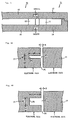
- FIG. 4 shows two examples of the configuration of the above grooves.
- a groove of depth d0 and thickness g0 is provided at a distance of h0 from the electrode face (the opposing faces of the upper and lower conductive plates).
- g0 is equal to the gap g between the conductive plates 15 and 17.
- h0 d0 , these lengths being an odd multiple of a quarter of the wavelength of the electromagnetic waves propagating through the gap.
- a point P2 which is a distance d0 from the end P3, is an equivalently open point
- a point P1 which is a distance h0 from the point P2 is an equivalently short-circuiting point (short-circuiting face). Therefore, the electrode faces of conductive plates 15 and 17 are equivalently continuous.
- the width g1 of the groove is wider than the gap g of the conductive plates 15 and 17.
- the position, depth, and width of the groove should be set so that the position of P1, as viewed from the short-circuited face P3, is an equivalently short-circuited face.
- the greater the width g1 of the groove the shorter the distance h1 from the electrode face to the groove, and consequently it is possible to make the point P2 portion between the two conductive plates an equivalently open point.
- the portion between the two conductive plates is made an open terminal in this manner, no current flows to the conductive plates, thereby reducing conductive loss.
- the two NRD guides comprising a moving portion and a fixed portion, are separated at the conductive plate portion, their electrode faces are equivalently continuous, and so almost no loss is caused by the presence of the gap. Furthermore, since there is almost no reflection in the space, no spurious mode is caused by reflection.
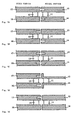
- FIGS. 5A to 5E show cross-sectional views of other configurations of a coupling portion between two NRD guides.
- grooves were provided in the end faces of both the upper and lower conductive plates; however, as shown in FIG. 5A, grooves can be provided not only in the fixed portion side but also in the moving portion side.
- grooves can be provided in opposite parts of the upper and lower conductive plates of the fixed portion and the moving portion.
- the grooves can be provided facing each other on both sides.
- the thicknesses of the conductive plates of the fixed portion and the moving portion do not necessarily have to be the same, but when they differ, the opposing end faces of the conductive plates should have the same thickness, as in FIG. 5D.
- the conductive plates 14 and 15 on the moving portion side are made thin overall, the overall size and weight of the moving portion can be made small, enabling it to be displaced easily using even a low-torque motor.
- a groove may be provided in just one of the conductive plates, to achieve a desired effect.
- g 0.2 mm
- g1 1.0 mm
- h1 0.96 mm
- d1 1.5 mm.
- the distance from the end P3 of the groove to the electrode face P1 was half the wavelength of the propagated waves, but this distance need only be n ⁇ /2, where n is a whole number greater than 1, and ⁇ is the wavelength.
- the distance from the electrode face P1 and the groove end P3 to the midpoint P2 should be (2m - 1) ⁇ /4 (where m is an integer greater than 1).
- FIG. 6 shows the relation between the directional coupler described above and the power splitting ratio.
- FIGS. 7A and 7B show the cross-sectional configurations of the hyper NRD guide and the normal NRD guide portion in the directional coupler shown in FIG. 1.
- FIG. 7A is a cross-sectional view of the NRD guide 12 taken along the line A-A of FIG. 1
- FIG. 7B is a cross-sectional view taken along the line B-B in FIG. 1.
- the space Dh between the electrode faces of the conductive plates 16 and 17 is equal to the height of the dielectric strip 12.
- grooves of depth Gh are provided in the conductive plates 16 and 17, so that the space Eh between the electrode faces of the conductive plates 16 and 17 is narrower than the height Dh of the dielectric strip 12'.
- the space between the propagation region of the dielectric strips and the conductive break plate in the nonpropagation region where there are no dielectric strips is determined, the dielectric constants of the dielectric strips are determined, and the cut-off frequency of the LSM01 mode is set lower than the cut-off frequency of the LSE01 mode, and the cut-off frequency of the LSE01 mode is set higher than the frequency used.
- the width DHw of the dielectric strip 12' of the hyper NRD guide is smaller than the width DNw of the dielectric strip 12 of the normal NRD guide.
- FIG. 8 is a perspective view of the configuration of a normal NRD guide, a hyper NRD guide, and a guide converter.
- FIG. 9 shows a top view and a cross-sectional view of the same.
- FIG. 8 and FIG. 9 show states when the upper conductive plate has been removed.
- the converter portion of the hyper NRD guide and the normal NRD guide is tapered so as to gradually eliminate the dimensional difference in the widths of the dielectric strips of the NRD guides.
- the space between the electrode faces of the conductive plates 16 and 17 changes in stages. That is, the space between the electrode faces of the hyper NRD guide does not change from the position of the interface between the hyper NRD guide and the converter to w1.
- the space between the electrode faces of the normal NRD guide does not change from the position of the interface between the normal NRD guide and the converter to w2.
- the spaces between the electrode faces of the normal NRD guide and the hyper NRD guide have an intermediate value.
- w0 3.0 mm
- gh1 0.13 mm
- gh2 0.37 mm.
- w3 corresponds to approximately one-quarter of the wavelength of the propagated waves. Consequently, a reflected wave 1 and a reflected wave 2 are coupled in reverse phase in the step portion of the space between the electrode faces, thereby cancelling the emitted waves.
- the hyper NRD guide and the normal NRD guide can be converted with no problem of reflection.
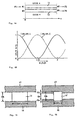
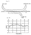
- FIGS. 10A to 10D show sizes of all the portions when the directional coupler described above is configured as an 0 dB directional coupler, and FIG. 11 shows its characteristics.
- FIGS. 10A to 10D show the dimensions of all the portions in millimeters.
- FIG. 10A is a top view when the upper conductive plate is removed
- FIG. 10B is a cross-sectional view taken along the line A-A of FIG. 10B
- FIG. 10C is a top view of the guide converter portion of the normal NRD guide and the hyper NRD guide and a cross-sectional view of the area near it.
- FIG. 10D is a diagram showing the original position of the moving portion.
- FIG. 11 is a diagram showing transparency characteristics of the directional coupler when the moving portion has been displaced by -8 mm, 0 mm and +8 mm to three different positions, FIG. 11A showing the transparency characteristics at each frequency, FIG. 11B being an enlarged view of the transparency characteristics to the primary emitter, and FIG. 11C showing changes in the transparency characteristics in relation to the position of the moving portion at 59.5 GHz.
- power can be split at approximately 0 dB. 0 dB is not achieved since, in addition to deviation in the power split, there are also guide loss and transmission loss.
- FIG. 12A is a top view of the state when the upper conductive plate is removed
- FIG. 12B is a cross-sectional view taken along the line A-A in FIG. 12A
- FIG. 12C is a cross-sectional view as a comparative example.
- one portion 11' of the dielectric strip 11 of the NRD guide on the moving portion side is a hyper NRD guide, and the other end portion 11'' is also a hyper NRD guide.
- this directional coupler is a 0 dB directional coupler, almost no transmission signals are output from the port #1 to the hyper NRD guide using the dielectric strip 11'' on the opposite side of the primary emitter 13, and consequently, since there is no need for resistance-termination, it can be used as an open terminal or as a short-circuiting terminal.
- the hyper NRD guide portion comprising the dielectric strip 11' which is coupled to the primary emitter 13 is provided close to the normal NRD guide of the fixed portion side, creating an electrical wall, but when the directional coupler is a 0 dB directional coupler, almost no electromagnetic waves propagate through this portion and so there is no problem of coupling to the LSE mode.
- an LSE mode suppresser should be provided inside the dielectric strip 12 of the normal NRD guide which is comparatively close to the hyper NRD guide, as shown in FIG. 13.
- FIG. 13B is a partially cross-sectional view in the vertical direction through the center of the dielectric strip 12
- FIG. 13C is a cross-sectional view taken along the line A - A of FIG. 13A.
- An LSE mode suppresser is basically a conductive member provided perpendicular to the electrode faces and parallel to the direction of wave propagation, for preventing LSE mode in this portion. Furthermore, the height of this conductive member is alternately changed to form a filter circuit, thereby ensuring that there is no coupling with the TEM mode.
- the diagram shows an example at the 60 GHz band, and dimensions are shown in millimeters.
- a terminator 20 is provided to the dielectric strip 11' portion of the hyper NRD guide on the moving portion side.
- the terminator 20 is provided to the hyper NRD guide, even when the coupling balance of the directional coupler is slightly inexact, resulting in reflection of waves from the port #3, the effects of such reflection can be reduced.
- the terminator portion is a considerable distance away from the dielectric strip 12 of the normal NRD guide on the fixed portion side, ensuring that there is no coupling between them. Consequently, it is not necessary to provide a bend to keep the terminator portion away from the normal NRD guide on the fixed portion side.
- the port of the NRD guide comprising the dielectric strip 11' can be used for other purposes.
- output terminals may be provided at port #2 and port #3, and transmission signal power and frequency and the like can be monitored from port #2, and the reflection at the antenna terminal can be monitored from port #3.
- FIGS. 14A to 14B are diagrams showing other examples of configurations of a directional coupler.
- a bend was provided in the hyper NRD guide coupled to the primary emitter on the moving portion side, but as shown in FIG. 14A, the primary emitter can be arranged without a bend.
- the polarized wave face of the primary emitter 13 is parallel to the direction in which the moving portion 31 moves. If a bend is provided and the primary emitter 13 is coupled at an angle of 45 degrees as in the previous examples, the electromagnetic wave polarized wave face tilts by 45 degrees. Therefore, the bend portion can be provided to suit the intended purpose.
- the entire NRD guide of the moving portion 31 can be a normal NRD guide. This will usually increase the size of the moving portion 31, so the radius of curvature of the bend should be set to minimize transmission loss when switching between modes.
- FIG. 15 is a cross-sectional view of another example configuration of the moving portion side of a directional coupler.
- the upper and lower conductive plates 14 and 15 are formed by plating the outer faces of synthetic resin plates with a metal film.
- the base material of the resin should be shaped in advance and the metal plating is applied to all the outer faces thereof, including the inner faces of the grooves. Since the electrode film acting as the NRD guide is on the faces clasping the dielectric strip 11 on either side, it is not essential to provide an electrode film on the outer faces.
- FIG. 16 is another example of a configuration of the moving portion, and shows a top view when the upper conductive plate is removed.
- the range (area) of the conductive plates has been reduced as far as possible in regions other than the positions of the primary emitter 13 and the dielectric strips 11 and 11' provided to the moving portion 31.
- notches are provided as shown at A and B, and a hole is provided as shown at C. These should be limited within a range which does not affect the NRD guide characteristics and the primary emitter characteristics.
- the notches and the hole are provided at least 2 mm in the width direction from the dielectric strip 11', and at least 8 mm from the primary emitter 13.
- the secure range is represented by a broken line.
- FIG. 17 is a top view when the upper conductive plate portion is removed.
- the configuration of the directional coupler in the moving portion 31 and the fixed portion 32 is the same as FIG. 1.
- the port #1 is the signal input/output portion of the directional coupler and connects to a circulator 19.
- a hyper NRD guide comprising a dielectric strip 21 connects to the input port of the circulator 19, and a hyper NRD guide comprising a dielectric strip 23 connects to the output port of the circulator 19.
- An oscillator is connected to the hyper NRD guide comprising the dielectric strip 21, and a mixer is connected to the hyper NRD guide comprising the dielectric strip 23.
- a dielectric strip 22 is provided between the dielectric strips 21 and 23 and is coupled to the hyper NRD guides, comprising the dielectric strips 21 and 23 respectively, thereby forming a directional coupler.
- Terminators 20 are provided at both ends of the dielectric strip 22.
- the mixer and the oscillator comprising a hyper NRD guide with a substrate in between to provide a circuit for applying bias voltage to these diodes comprises a varactor diode and a Gunn diode.
- the oscillating signal of the oscillator is sent from the dielectric strip 21 ⁇ the circulator 19 ⁇ the dielectric strip 12 ⁇ the dielectric strip 11 ⁇ the primary emitter 13.
- electromagnetic waves received at the primary emitter 13 are sent from the dielectric strip 11 ⁇ the dielectric strip 12 ⁇ the circulator 19 ⁇ the dielectric strip 23, and are finally input to the mixer.
- part of the oscillating signal is sent as a local signal to the mixer together with the received signal, via the two directional couplers comprising the dielectric strips 21, 22 and 23. Consequently, the mixer outputs the frequency components of the difference between the transmitted signal and the received signal as an intermediate-frequency signal.
- FIG. 18 is an exploded perspective view of an overall configuration of a transceiver.
- a moving portion drive unit 42 for displacing the moving portion 31 will be explained below.
- a horn 43 has an opening, comprising a long hole extending in the direction which the moving portion 31 is displaced in.
- the moving portion 31 and a "0 dB coupler" form a directional coupler.
- a circuit portion RF comprises the above mixer, and a circuit portion VCO comprises the above oscillator.
- a controller controls the moving portion drive unit 42, extracts information based on the intermediate-frequency signal including the distance, angle and relative speed of the moving portion drive unit 42, and sends these data to an external device.
- FIG. 19 is a perspective view of the configuration of the moving portion drive unit.
- one end of a forward screw 54 is attached via a bearing to a frame so that the forward screw 54 can rotate freely.
- the other end of the forward screw 54 connects to the axis of a pulse motor 55 which is securely screwed to the frame.
- the frame has a forward guide 51 which is parallel to the forward screw 54, and the forward screw 54 screws into a nut portion which can slide along the forward guide 51.
- the moving portion 31 has a primary emitter and is securely screwed to the nut portion.
- an interceptor plate 52 is attached to the nut portion.
- the frame has a photointerrupter 53, and the interceptor plate 52 passes through the optical axis of the photointerrupter 53.
- This forward screw system is basically open-loop controlled, since the moving portion 31 is displaced to a predetermined position by applying a predetermined number of pulses to the pulse motor 55. That is, a CPU controls the pulse of the pulse motor by applying a predetermined number of pulses to the pulse motor, thereby controlling the position of the moving portion. Simultaneously, a memory or register counts the pulse number representing the present position of the moving portion, thereby indirectly detecting the position of the moving portion. Since the position of the moving portion 31 cannot be detected immediately after power injection or when the pulse motor has malfunctioned, in such cases its position is detected using the interceptor plate 52 and the photointerrupter 53.
- FIGS. 20A and 20B show the configuration of the moving portion drive unit in such a case.
- FIG. 20A is a perspective view
- FIG. 20B is a cross-sectional view through the face perpendicular to the displacement direction of the moving portion.
- a magnetic circuit comprises external yokes 46 and 47, an internal yoke 45, and magnets 48 and 49, attached to the inner faces of the external yokes 46 and 47.
- Two guide pins 51 and 51 are secured to the external yoke 47 and are parallel to the internal yoke 45.
- a moving coil 50 is provided in a single body with a moving push portion, which slides along the guide pins 51 and 51. Simultaneously, the internal yoke 45 passes through the moving coil 50 while maintaining a fixed distance thereto.
- the moving portion 31 comprising a primary emitter is securely screwed to the moving push portion.
- An interceptor plate 52 is attached to the moving push portion and has a rhombic window.
- Two photointerrupters 53a and 53b are attached to the external yoke 47, so that their optical axes pass through the rhombic window.
- the position of the moving portion 31 is detected in accordance with the difference in the amounts of light received by the two photointerrupters 53a and 53b, and the motor is driven to move the moving portion 31 to a predetermined position.
- FIG. 21 is a block diagram showing an overall configuration of a milliwave radar comprising the antenna device and the transceiver described above.
- a signal processing portion in a signal processor uses a transceiver to detect numerical data such as, for instance, the relative speed and distance to a vehicle traveling in front. Then, based on the relation between the traveling speed of the main vehicle and the distance between the main vehicle and the vehicle in front, a control/warning portion issues a warning when, for instance, predetermined conditions are satisfied, or issues a warning when the speed relative to the vehicle in front has exceeded a predetermined threshold value.
- FIG. 25 is a partial perspective view of a configuration of the aligned portion of two upper conductive plates.
- plane waves propagating through the space are considered to include not only waves transmitted perpendicular to the electrode faces (direction x) but also waves propagating parallel to the length of the dielectric guide (the z direction) in the LSM mode, which is a main mode of the NRD guide.
- FIG. 25 plane waves propagating from point p1 shift to the y direction of the groove at point p2, and are then reflected from point p3 to point p4. After that, they are reflected yet again until they reach point p5.
- the points p1 and p5 of FIG. 25 correspond to the points P1 and P2 of FIG. 4
- point p2 and p4 correspond to point P2
- point p3 corresponds to point P3 of FIG. 4.
- ⁇ is the frequency
- ⁇ is the dielectric constant of the groove
- ⁇ is the permeability of the groove.
- k ⁇ ( ⁇ o ⁇ o ) .
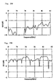
- FIG. 28 shows measurements of the characteristics of the directional coupler at this time.
- the ports of the directional coupler are defined as in FIG. 27.
- Fluorine resin with a specific dielectric constant of 2.04 was used as the dielectric material.
- FIG. 29A shows the transparency characteristic when no groove is provided.
- the LSM mode converts to the LSE mode at certain frequencies (in the example shown, approximately 73 GHz, 75 GHz, 77 GHz, 79 GHz, 81 GHz), resulting in severe loss.
- the device functions with the electrode faces of both conductive plates being equivalently continuous, and so there is almost no loss in the space between the conductive plates. Furthermore, since there is almost no reflection in the space, there are no spurious modes caused by reflection.
- a short-circuiting face is provided in an optimum position in correspondence with the direction of plane waves propagating through the portion where the end faces of the conductive plates of the first and second dielectric guides are aligned, whereby reflection in the aligned portion of the conductive plates can be most effectively reduced.
- nonradiative dielectric guide portion Furthermore, according to a first type of nonradiative dielectric guide portion, coupling is possible without making the space between dielectric strips extremely narrow. In addition, according to a second type of nonradiative dielectric guide portion, even though a bend of small radius of curvature is provided, there is no conversion from LSM mode to LSE, whereby the entire device can easily be made small without increasing transmission loss.
- the present invention provides an antenna device wherein the direction of the beam is tilted by relatively displacing a first dielectric guide with respect to a second dielectric guide, so that there is low loss in the directional coupler portion. Moreover, by providing first and second types of nonradiative dielectric guide portions on the dielectric guide side, the moving portion can be made small and of low mass, so that the beam can be tilted quickly even when a low-torque motor is used. Furthermore, by providing first and second types of nonradiative dielectric guide portions on the second dielectric guide side, an antenna device which is miniturized overall can be obtained.
- transmission signals and received signals can be electrically transmitted with maximum efficiency between a moving portion and a fixed portion, increasing the efficiency of the antenna.
- the present invention also provides a miniturized antenna for transmitting and receiving, wherein the direction of the beam can be tilted using a single primary emitter and a single directional coupler.
- the present invention provides a transceiver which is miniturized and has low loss.
Landscapes
- Waveguides (AREA)
- Aerials With Secondary Devices (AREA)
- Variable-Direction Aerials And Aerial Arrays (AREA)
- Waveguide Switches, Polarizers, And Phase Shifters (AREA)
- Non-Reversible Transmitting Devices (AREA)
Applications Claiming Priority (4)
| Application Number | Priority Date | Filing Date | Title |
|---|---|---|---|
| JP18950898 | 1998-07-03 | ||
| JP18950898 | 1998-07-03 | ||
| JP37380898A JP3498611B2 (ja) | 1998-07-03 | 1998-12-28 | 方向性結合器、アンテナ装置および送受信装置 |
| JP37380898 | 1998-12-28 |
Publications (3)
| Publication Number | Publication Date |
|---|---|
| EP0969545A2 true EP0969545A2 (fr) | 2000-01-05 |
| EP0969545A3 EP0969545A3 (fr) | 2002-04-24 |
| EP0969545B1 EP0969545B1 (fr) | 2005-01-26 |
Family
ID=26505509
Family Applications (1)
| Application Number | Title | Priority Date | Filing Date |
|---|---|---|---|
| EP99112473A Expired - Lifetime EP0969545B1 (fr) | 1998-07-03 | 1999-06-30 | Coupleur directionnel, dispositif d' antenne, et émetteur-récepteur |
Country Status (5)
| Country | Link |
|---|---|
| US (1) | US6172648B1 (fr) |
| EP (1) | EP0969545B1 (fr) |
| JP (1) | JP3498611B2 (fr) |
| CA (1) | CA2276834C (fr) |
| DE (1) | DE69923383T2 (fr) |
Cited By (3)
| Publication number | Priority date | Publication date | Assignee | Title |
|---|---|---|---|---|
| EP0971436A3 (fr) * | 1998-07-06 | 2001-11-07 | Murata Manufacturing Co., Ltd. | Dispositif d antenne et appareil d émission/réception |
| FR2813995A1 (fr) * | 2000-09-08 | 2002-03-15 | Murata Manufacturing Co | Coupleur directionnel, dispositif d'antenne et systeme de radar |
| RU2585884C1 (ru) * | 2015-03-11 | 2016-06-10 | Федеральное государственное бюджетное образовательное учреждение высшего профессионального образования "Томский государственный университет систем управления и радиоэлектроники" | Транснаправленный ответвитель на связанных линиях с вертикальной платой |
Families Citing this family (8)
| Publication number | Priority date | Publication date | Assignee | Title |
|---|---|---|---|---|
| JP3498597B2 (ja) * | 1998-10-22 | 2004-02-16 | 株式会社村田製作所 | 誘電体線路変換構造、誘電体線路装置、方向性結合器、高周波回路モジュールおよび送受信装置 |
| DE19963625A1 (de) * | 1999-12-29 | 2001-07-12 | Bosch Gmbh Robert | Verfahren zur Messung des Abstands und der Geschwindigkeit von Objekten |
| JP2002246832A (ja) * | 2001-02-15 | 2002-08-30 | Matsushita Electric Ind Co Ltd | 通信装置 |
| US6563456B1 (en) * | 2001-10-04 | 2003-05-13 | Yazaki North America, Inc. | Flexible wave guide joint |
| US6480160B1 (en) * | 2001-10-09 | 2002-11-12 | Yazaki North America, Inc. | Radar apparatus including a wave guide array and a dielectric lens |
| KR100539493B1 (ko) * | 2002-12-18 | 2005-12-29 | 한국전자통신연구원 | 비방사 유전체 도파로를 이용한 방향성 결합기 |
| KR100702204B1 (ko) | 2006-02-06 | 2007-04-03 | 서울시립대학교 산학협력단 | 신호반사포트를 구비한 rfid용 방향성 결합기 |
| EP4329087A1 (fr) * | 2022-08-26 | 2024-02-28 | indie Semiconductor FFO GmbH | Interface de données de guide d'ondes diélectrique et système de capteur |
Family Cites Families (8)
| Publication number | Priority date | Publication date | Assignee | Title |
|---|---|---|---|---|
| US2751556A (en) * | 1950-11-22 | 1956-06-19 | Sperry Rand Corp | Variable transfer directional coupler for microwave energy |
| US2837723A (en) * | 1953-05-11 | 1958-06-03 | Frank M Krantz | Waveguide coupling |
| US2830276A (en) * | 1954-06-25 | 1958-04-08 | Gen Precision Lab Inc | Microwave rotary joint |
| US5041839A (en) * | 1981-03-11 | 1991-08-20 | The Secretary Of State For Defence In Her Britannic Majesty's Government Of The United Kingdom Of Great Britain And Northern Ireland | Electromagnetic radiation sensors |
| JP3045046B2 (ja) * | 1995-07-05 | 2000-05-22 | 株式会社村田製作所 | 非放射性誘電体線路装置 |
| JP3018987B2 (ja) * | 1996-07-08 | 2000-03-13 | 株式会社村田製作所 | 誘電体線路集積回路 |
| JPH1065413A (ja) * | 1996-08-19 | 1998-03-06 | Murata Mfg Co Ltd | 誘電体線路型方向性結合器 |
| US5933120A (en) * | 1996-12-16 | 1999-08-03 | Waveband Corporation | 2-D scanning antenna and method for the utilization thereof |
-
1998
- 1998-12-28 JP JP37380898A patent/JP3498611B2/ja not_active Expired - Fee Related
-
1999
- 1999-06-30 EP EP99112473A patent/EP0969545B1/fr not_active Expired - Lifetime
- 1999-06-30 DE DE69923383T patent/DE69923383T2/de not_active Expired - Lifetime
- 1999-07-02 US US09/346,815 patent/US6172648B1/en not_active Expired - Lifetime
- 1999-07-05 CA CA002276834A patent/CA2276834C/fr not_active Expired - Fee Related
Cited By (6)
| Publication number | Priority date | Publication date | Assignee | Title |
|---|---|---|---|---|
| EP0971436A3 (fr) * | 1998-07-06 | 2001-11-07 | Murata Manufacturing Co., Ltd. | Dispositif d antenne et appareil d émission/réception |
| FR2813995A1 (fr) * | 2000-09-08 | 2002-03-15 | Murata Manufacturing Co | Coupleur directionnel, dispositif d'antenne et systeme de radar |
| US6542046B2 (en) | 2000-09-08 | 2003-04-01 | Murata Manufacturing Co. Ltd. | Directional coupler, antenna device, and radar system |
| KR100493810B1 (ko) * | 2000-09-08 | 2005-06-08 | 가부시키가이샤 무라타 세이사쿠쇼 | 방향성 결합기, 안테나 장치 및 레이더 시스템 |
| DE10143688B4 (de) * | 2000-09-08 | 2009-02-19 | Murata Mfg. Co., Ltd., Nagaokakyo-shi | Richtungskoppler, Antennenvorrichtung und Radarsystem |
| RU2585884C1 (ru) * | 2015-03-11 | 2016-06-10 | Федеральное государственное бюджетное образовательное учреждение высшего профессионального образования "Томский государственный университет систем управления и радиоэлектроники" | Транснаправленный ответвитель на связанных линиях с вертикальной платой |
Also Published As
| Publication number | Publication date |
|---|---|
| JP3498611B2 (ja) | 2004-02-16 |
| CA2276834C (fr) | 2002-09-03 |
| JP2000082904A (ja) | 2000-03-21 |
| DE69923383D1 (de) | 2005-03-03 |
| CA2276834A1 (fr) | 2000-01-03 |
| DE69923383T2 (de) | 2006-03-30 |
| US6172648B1 (en) | 2001-01-09 |
| EP0969545B1 (fr) | 2005-01-26 |
| EP0969545A3 (fr) | 2002-04-24 |
Similar Documents
| Publication | Publication Date | Title |
|---|---|---|
| JP3473576B2 (ja) | アンテナ装置および送受信装置 | |
| JP3186622B2 (ja) | アンテナ装置および送受信装置 | |
| US7212087B2 (en) | Twisted waveguide and wireless device | |
| US6433741B2 (en) | Directional coupler, antenna device, and transmitting-receiving device | |
| EP0871239B1 (fr) | Dispositif d'antenne et module de radar | |
| US6008755A (en) | Antenna-shared distributor and transmission and receiving apparatus using same | |
| KR100270038B1 (ko) | 송수신장치 | |
| JP2002111359A (ja) | アンテナ装置、通信装置およびレーダ装置 | |
| CA2276834C (fr) | Coupleur directif, dispositif d'antenne et emetteur-recepteur | |
| US6133887A (en) | Antenna device, and transmitting/receiving unit | |
| CA2256283C (fr) | Guide d'ondes dielectrique non radiatif comprenant une partie pour la conversion de ligne entre differents types de guides d'ondes dielectriques non radiatifs | |
| JP2002084111A (ja) | 方向性結合器、アンテナ装置およびレーダ装置 | |
| JP3485054B2 (ja) | 異種非放射性誘電体線路変換部構造およびその装置 | |
| JP3846585B2 (ja) | 導波管ベンド、導波管プレートおよび高周波装置 | |
| JP3617397B2 (ja) | 誘電体線路導波管変換器、誘電体線路接続構造、1次放射器、発振器および送信装置 | |
| US6342863B2 (en) | Antenna apparatus and antenna and tranceiver using the same | |
| JP3259637B2 (ja) | 送受信装置 |
Legal Events
| Date | Code | Title | Description |
|---|---|---|---|
| PUAI | Public reference made under article 153(3) epc to a published international application that has entered the european phase |
Free format text: ORIGINAL CODE: 0009012 |
|
| 17P | Request for examination filed |
Effective date: 19990630 |
|
| AK | Designated contracting states |
Kind code of ref document: A2 Designated state(s): AT BE CH CY DE DK ES FI FR GB GR IE IT LI LU MC NL PT SE Kind code of ref document: A2 Designated state(s): DE FR GB |
|
| AX | Request for extension of the european patent |
Free format text: AL;LT;LV;MK;RO;SI |
|
| PUAL | Search report despatched |
Free format text: ORIGINAL CODE: 0009013 |
|
| AK | Designated contracting states |
Kind code of ref document: A3 Designated state(s): AT BE CH CY DE DK ES FI FR GB GR IE IT LI LU MC NL PT SE |
|
| AX | Request for extension of the european patent |
Free format text: AL;LT;LV;MK;RO;SI |
|
| RIC1 | Information provided on ipc code assigned before grant |
Free format text: 7H 01P 5/18 A, 7H 01P 1/06 B |
|
| AKX | Designation fees paid |
Free format text: DE FR GB |
|
| 17Q | First examination report despatched |
Effective date: 20031028 |
|
| GRAP | Despatch of communication of intention to grant a patent |
Free format text: ORIGINAL CODE: EPIDOSNIGR1 |
|
| GRAS | Grant fee paid |
Free format text: ORIGINAL CODE: EPIDOSNIGR3 |
|
| GRAA | (expected) grant |
Free format text: ORIGINAL CODE: 0009210 |
|
| AK | Designated contracting states |
Kind code of ref document: B1 Designated state(s): DE FR GB |
|
| REG | Reference to a national code |
Ref country code: GB Ref legal event code: FG4D |
|
| REG | Reference to a national code |
Ref country code: IE Ref legal event code: FG4D |
|
| REF | Corresponds to: |
Ref document number: 69923383 Country of ref document: DE Date of ref document: 20050303 Kind code of ref document: P |
|
| PLBE | No opposition filed within time limit |
Free format text: ORIGINAL CODE: 0009261 |
|
| STAA | Information on the status of an ep patent application or granted ep patent |
Free format text: STATUS: NO OPPOSITION FILED WITHIN TIME LIMIT |
|
| 26N | No opposition filed |
Effective date: 20051027 |
|
| ET | Fr: translation filed | ||
| PGFP | Annual fee paid to national office [announced via postgrant information from national office to epo] |
Ref country code: GB Payment date: 20130626 Year of fee payment: 15 Ref country code: DE Payment date: 20130626 Year of fee payment: 15 |
|
| PGFP | Annual fee paid to national office [announced via postgrant information from national office to epo] |
Ref country code: FR Payment date: 20130624 Year of fee payment: 15 |
|
| REG | Reference to a national code |
Ref country code: DE Ref legal event code: R119 Ref document number: 69923383 Country of ref document: DE |
|
| GBPC | Gb: european patent ceased through non-payment of renewal fee |
Effective date: 20140630 |
|
| REG | Reference to a national code |
Ref country code: FR Ref legal event code: ST Effective date: 20150227 |
|
| REG | Reference to a national code |
Ref country code: DE Ref legal event code: R119 Ref document number: 69923383 Country of ref document: DE Effective date: 20150101 |
|
| PG25 | Lapsed in a contracting state [announced via postgrant information from national office to epo] |
Ref country code: DE Free format text: LAPSE BECAUSE OF NON-PAYMENT OF DUE FEES Effective date: 20150101 |
|
| PG25 | Lapsed in a contracting state [announced via postgrant information from national office to epo] |
Ref country code: GB Free format text: LAPSE BECAUSE OF NON-PAYMENT OF DUE FEES Effective date: 20140630 Ref country code: FR Free format text: LAPSE BECAUSE OF NON-PAYMENT OF DUE FEES Effective date: 20140630 |