EP0970538B1 - Antenne a balayage a reflecteur - Google Patents
Antenne a balayage a reflecteur Download PDFInfo
- Publication number
- EP0970538B1 EP0970538B1 EP98953236A EP98953236A EP0970538B1 EP 0970538 B1 EP0970538 B1 EP 0970538B1 EP 98953236 A EP98953236 A EP 98953236A EP 98953236 A EP98953236 A EP 98953236A EP 0970538 B1 EP0970538 B1 EP 0970538B1
- Authority
- EP
- European Patent Office
- Prior art keywords
- antenna
- electrically
- dielectric layer
- controllable
- reflecting surface
- Prior art date
- Legal status (The legal status is an assumption and is not a legal conclusion. Google has not performed a legal analysis and makes no representation as to the accuracy of the status listed.)
- Expired - Lifetime
Links
- 238000000034 method Methods 0.000 title description 16
- 239000003989 dielectric material Substances 0.000 claims description 15
- 230000004044 response Effects 0.000 claims description 7
- 239000003302 ferromagnetic material Substances 0.000 claims 1
- 238000004891 communication Methods 0.000 description 50
- 239000000463 material Substances 0.000 description 9
- 230000010363 phase shift Effects 0.000 description 6
- 229910052454 barium strontium titanate Inorganic materials 0.000 description 5
- 230000002452 interceptive effect Effects 0.000 description 5
- 238000010586 diagram Methods 0.000 description 4
- 230000005855 radiation Effects 0.000 description 4
- 230000003044 adaptive effect Effects 0.000 description 3
- 230000008859 change Effects 0.000 description 3
- 230000008569 process Effects 0.000 description 3
- 238000001228 spectrum Methods 0.000 description 3
- 230000005684 electric field Effects 0.000 description 2
- 238000012986 modification Methods 0.000 description 2
- 230000004048 modification Effects 0.000 description 2
- 206010035148 Plague Diseases 0.000 description 1
- 241000607479 Yersinia pestis Species 0.000 description 1
- 238000003491 array Methods 0.000 description 1
- 230000015572 biosynthetic process Effects 0.000 description 1
- 239000004020 conductor Substances 0.000 description 1
- 230000000694 effects Effects 0.000 description 1
- 230000005670 electromagnetic radiation Effects 0.000 description 1
- 238000005516 engineering process Methods 0.000 description 1
- 238000005286 illumination Methods 0.000 description 1
- 238000002955 isolation Methods 0.000 description 1
- 229910052751 metal Inorganic materials 0.000 description 1
- 239000002184 metal Substances 0.000 description 1
- 230000003287 optical effect Effects 0.000 description 1
- 230000010287 polarization Effects 0.000 description 1
- 238000000926 separation method Methods 0.000 description 1
- 239000000758 substrate Substances 0.000 description 1
- 230000001360 synchronised effect Effects 0.000 description 1
Images

Classifications
-
- H—ELECTRICITY
- H01—ELECTRIC ELEMENTS
- H01Q—ANTENNAS, i.e. RADIO AERIALS
- H01Q25/00—Antennas or antenna systems providing at least two radiating patterns
-
- H—ELECTRICITY
- H01—ELECTRIC ELEMENTS
- H01Q—ANTENNAS, i.e. RADIO AERIALS
- H01Q15/00—Devices for reflection, refraction, diffraction or polarisation of waves radiated from an antenna, e.g. quasi-optical devices
- H01Q15/14—Reflecting surfaces; Equivalent structures
- H01Q15/148—Reflecting surfaces; Equivalent structures with means for varying the reflecting properties
-
- H—ELECTRICITY
- H01—ELECTRIC ELEMENTS
- H01Q—ANTENNAS, i.e. RADIO AERIALS
- H01Q3/00—Arrangements for changing or varying the orientation or the shape of the directional pattern of the waves radiated from an antenna or antenna system
- H01Q3/44—Arrangements for changing or varying the orientation or the shape of the directional pattern of the waves radiated from an antenna or antenna system varying the electric or magnetic characteristics of reflecting, refracting, or diffracting devices associated with the radiating element
Definitions
- This invention relates generally to reflective antennas and, more particularly, to an electronic scanning reflector antenna and method for using same.
- Space-based and terrestrial-based communication systems must share a limited frequency spectrum.
- the need to constantly increase the capacity of space-based and terrestrial-based communications systems has resulted in the continuing evolution of antenna technology.
- Antennas provide multiple beams using spatial and/or polarization isolation techniques. Advances are still required to provide enhanced performance with respect to providing adaptive antenna beam patterns.
- Adaptive antenna patterns have been generated using a variety of active and passive phased arrays.
- Communication systems have used phased array antennas to communicate with multiple users through multiple antenna beams.
- efficient bandwidth modulation techniques are combined with multiple access techniques, and frequency separation methods are employed to increase the number of users.
- US-A-5,262,796 discloses a scanning microwave antenna having an array of optically-controllable reflecting elements mounted on a dielectric substrate.
- An optical system for selective illumination of the photoconductive elements is used to make the elements change their co-efficients of reflection, thereby modifying an incident microwave beam.
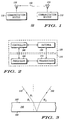
- FIG. 1 shows a simplified block diagram of a communication system within which the apparatus and methods of the present invention can be practiced.
- FIG. 1 illustrates two communications devices 110.
- Two antenna subsystems 120 are coupled to the communication devices for establishing a communication link 150 between the two communication devices.
- Antenna subsystems 120 comprise at least one electronically controllable antenna in a typical spectrum sharing scenario. As illustrated, there is, typically, at least one line-of-sight path between the communication devices.
- Communication devices 110 can be space-based and terrestrial-based communication devices.
- Space-based communication devices may reside in geostationary or non-geostationary orbits. In geostationary orbits, space-based communication devices remain relatively stationary to any given point on the surface of the earth. In non-geostationary orbits, space-based communication devices can move at high speed relative to any given point on the surface of the earth. In non-geostationary orbits, space-based communication devices can move at high speed relative to a space-based communication device in a geostationary orbit.
- Terrestrial-based communication devices are located proximate to the surface of the earth. The relative speeds between moving devices and relatively stationary devices mean that the communication devices have to dynamically alter the characteristics of their transmit and receive antenna beam patterns. In particular, antenna beam pointing directions are dynamically changing.
- Antenna subsystems 120 alter antenna beam patterns and vary the pointing directions over a wide angle field of view.
- Antenna beam pattern requirements are different for communication devices operating in different environments.
- the antenna pattern required by a space-based communication device is different from the antenna pattern required by a terrestrial-based communication device.
- a communication device located in a geostationary orbit has different antenna pattern requirements than a communication device located in a non-geostationary orbit.
- Interference paths are a problem in most communication system. Undesired line-of-sight paths can exist between communication devices 110.
- Communication devices 110 desirably employ electronic scanning reflector antennas (ESRA) to mitigate the interference problem.
- ESRA electronic scanning reflector antennas
- Communication devices 110 communicate with other communication devices 110 using radio frequency (RF) communication links 150.
- Communication devices 110 are preferably configured to communicate using time-division multiple access (TDMA), frequency-division multiple access (FDMA), code-division multiple access (CDMA) methods, or a combination thereof.
- TDMA time-division multiple access
- FDMA frequency-division multiple access
- CDMA code-division multiple access
- FIG. 2 shows a simplified block diagram of communication device 110 and antenna subsystem 120 in accordance with a preferred embodiment of the present invention.
- Communication device 110 comprises at least one transceiver 170 and at least one processor 160 which is coupled to transceiver 170.
- Antenna subsystem 120 comprises at least one antenna 190 and at least one controller 180 which is coupled to antenna 190.
- Antenna 190 (as illustrated) is coupled to transceiver 170. Controller 180 (as illustrated) is coupled to processor 160. Antenna 190 is desirably an electronic scanning reflector antenna. Controller 180 implements the necessary control functions which cause antenna 190 to form antenna beams with the desired characteristics.
- RF signals are transferred between antenna 190 and transceiver 170.
- the signal path is illustrated as a single line, many interconnections are possible between antenna 190 and transceiver 170.
- Digital data signals are transferred between controller 180 and antenna 190.
- transceiver 170 converts the RF signals received from antenna 190 into digital data.
- transceiver 170 converts digital data obtained from processor 160 into RF signals.
- the RF signals are sent to antenna 190 by transceiver 170.
- Control signals are transferred between controller 180 and processor 160.
- Digital data signals are also transferred between processor 160 and transceiver 170.
- RF signals received by transceiver 170 are converted to digital data which is sent to processor 160 to be further processed.
- Antenna 190 includes elements (not shown in FIG. 2) preferably arranged in a two-dimensional array; however, other array configurations are suitable.
- RF signals are altered in the receive and transmit modes at the element level.
- FIG. 3 illustrates the reflecting and refracting properties associated with a dielectric layer applied over a reflecting surface in accordance with a preferred embodiment of the present invention.
- Incident wave 310 is assumed to be a plane wave, and surfaces 320 and 330 are assumed to be large with respect to the wavelength of the plane wave.
- the two angles shown for the incident wave are known as the angle of incidence ⁇ 1 and the elevation angle ⁇ 1 .
- the angle of incidence ⁇ 1 is the angle between the direction of propagation and a line normal to the surface.
- the elevation angle ⁇ 1 is the angle between the direction of propagation for the incident wave and the surface boundary.
- the components of the E field and the H field are continuous. In other words, the phase of the reflected wave is synchronous with the phase of the incident wave.
- Resultant wave 350 has an elevation angle ⁇ 2 .
- Dielectric layer 340 causes ⁇ 2 to be different from ⁇ 1 . Varying the dielectric constant of layer 340 causes elevation angle ⁇ 2 to change.
- FIG. 4 illustrates a top view for an electronic scanning reflector antenna in accordance with a preferred embodiment of the present invention.
- FIG. 5 illustrates a side view for an electronic scanning reflector antenna in accordance with a preferred embodiment of the present invention.
- ESRA 400 comprises antenna feeder 410, RF reflecting surface 420, and an electrically-controllable dielectric layer 430 applied to RF reflecting surface 420.
- electrically-controllable dielectric layer 430 is a voltage variable dielectric material.
- the voltage variable dielectric material has a dielectric constant which changes in response to a direct current (DC) voltage that is applied to the material.
- Antenna feeder 410 and reflecting surface 420 may be coupled using various body structures (not shown).
- Antenna feeder 410 may comprise a single or multiple sources.
- antenna feeder 410 is a single hom, and in other embodiments, antenna feeder 410 comprises several horn elements. In alternate embodiments, antenna feeder 410 is offset. In these cases, antenna feeder 410 and reflecting surface 420 are attached to a body structure (not shown), and antenna feeder 410 is located offset from the centerline of reflecting surface 420.
- RF reflecting surface 420 comprises a plurality of individual elements 450.
- individual elements 450 are attached to a carrier surface to form an array.
- RF reflecting surface 420 is an electrical conductor, desirably a metal.
- RF reflecting surface 420 is used to provide one of the electrodes needed to establish an electric field across dielectric layer 430.
- RF reflecting surface 420 is a substantially continuous surface. In this case, RF reflecting surface 420 can be maintained at a single potential such as ground.
- the ESRA has advantages over conventional fixed beam antennas because it can, among other things, provide greater viewing angles, adaptively adjust antenna beam patterns, provide antenna beams to individual users, provide antenna beams in response to demand for communication services and improve pattern nulling of unwanted RF signals. These features are implemented through appropriate software procedures performed in controller 180 (FIG. 2).
- electrically-controllable dielectric layer 430 is a current variable dielectric material.
- the current variable dielectric material has a dielectric constant which changes in response to a DC current that is applied to the material.
- the top view of ESRA 400 (FIG. 4) illustrates a preferred method for dividing dielectric layer 430 into smaller regions 450 which are independently controlled to produce the desired phase relationship to steer the antenna beams in any direction. This steering is accomplished by applying control voltages to the small regions of dielectric material. This allows antenna beams to be controlled faster than with a mechanical configuration. This ability allows hand-offs to take place faster. Since individual regions 450 of the antenna are controlled independently, ESRA 400 operates like a phased array antenna. ESRA 400, however, does not require costly discrete phase shift circuits at each element.
- multiple regions 450 are grouped together in rows and/or columns, and these rows and/or columns are controlled as groups.
- Superposition can be employed to provide each element a unique voltage and/or current required for the proper RF phase shift.
- individual regions 450 can have different shapes than those illustrated in FIG. 4.
- individual array elements can be any polygonal shape. Circles and/or ellipses can also be used.
- the number of regions 450 can be changed.
- a simple antenna can comprise a single region 450, and this single region can have a variety of shapes.
- individual regions 450 do not touch each other.
- Small gaps are present to allow the placement of electrodes.
- the electrodes are used to establish an electric field in the dielectric layer 430.
- gaps can be present between the individual regions or not. In addition, these gaps can vary in size and shape.
- substantially all of RF reflecting surface 420 is covered with dielectric layer 430.
- RF reflecting surface 420 is partially covered by electrically-controllable dielectric layer 430.
- some individual regions 450 can be covered with dielectric layer 430, and other individual regions 450 can be left uncovered.
- dielectric layer 430 comprises a single type of electrically-controllable dielectric material.
- the entire RF reflecting surface is not covered by the same type of electrically-controllable dielectric material. For example, some individual regions 450 are covered with a first material, and some individual regions 450 are covered with a second material.
- electrically-controllable dielectric 430 has a substantially uniform thickness across the face of the individual regions.
- individual regions 450 have a substantially uniform thickness for the electrically-controllable dielectric.
- the thickness of the electrically-controllable dielectric varies across the individual regions. In some cases, the variation in thickness follows a linear relationship. In other cases, there is a non-linear relationship for the thickness of the electrically-controllable dielectric. In other alternate embodiments, the thickness for the electrically-controllable dielectric varies for different individual regions. In some cases, the electrically-controllable dielectric is thicker for the individual regions located near the center of the array pattern. In other cases, the electrically-controllable dielectric is thicker for the individual regions located near the edge of the array pattern.
- electromagnetic radiation experiences a round trip phase shift that is twice the effective phase shift of the dielectric layer because the radiation passes through the layer twice.
- electrically-controllable dielectric 430 is a ferroelectric material, preferably based on Barium Strontium Titanate (BST).
- BST Barium Strontium Titanate
- a dielectric matching layer (not shown) is used between the BST and free-space. Since BST has a high relative dielectric constant, a dielectric matching layer is used to minimize reflections.
- the dielectric matching layer has a thickness which is approximately one quarter wavelength.
- the matching layer desirably has a dielectric constant which is approximately equal to the square root of BST.
- the dielectric constant for the matching layer is calculated using the geometric mean of the relative dielectric constants of the two media.
- FIG. 6 illustrates a top view for an electronic scanning reflector antenna in accordance with a first alternate embodiment of the present invention.
- FIG. 7 illustrates a side view for an electronic scanning reflector antenna in accordance with a first alternate embodiment of the present invention.
- ESRA 600 comprises antenna feeder 610, a first RF reflecting surface 620, a second RF reflecting surface 670, an electrically-controllable dielectric layer 630 applied to first RF reflecting surface 620, and body structure 660.
- body structure 660 may be a radome.
- the voltage variable dielectric material has a dielectric constant which changes in response to a DC voltage that is applied to the material.
- electrically-controllable dielectric layer 630 is a current variable dielectric material.
- the current variable dielectric material has a dielectric constant which changes in response to a DC current that is applied to the material.
- the top view of ESRA 600 (FIG. 6) illustrates a preferred method for dividing dielectric layer 630 into smaller regions 650 which are independently controlled to produce the desired phase relationship to steer the antenna beams in any direction. This steering is accomplished by applying control voltages to the small regions of dielectric material, and this allows antenna beams to be changed faster than a mechanical configuration. Since individual regions 650 of ESRA 600 are controlled independently, ESRA 600 operates like a phased array antenna. ESRA 600, however, does not require costly discrete phase shift circuits at each element.
- multiple regions 650 are grouped together in rows and/or columns, and these rows and/or columns are controlled as groups.
- Superposition can be employed to provide each element a unique voltage and/or current required for the proper RF phase shift.
- the individual regions may have different shapes than those illustrated in FIG. 6.
- individual array elements can be any polygonal shape. Circles and/or ellipses can also be used.
- the number of regions 650 can be changed.
- a simple antenna may comprise a single region 650, and this single region may have a variety of shapes.
- individual areas 650 do not touch each other. Gaps may be present between the individual areas. These gaps can vary in size and shape.
- RF reflecting surface 620 is covered with dielectric layer 630.
- RF reflecting surface 620 is partially covered by electrically-controllable dielectric layer 630.
- some individual regions 650 can be covered with a dielectric layer, and other individual regions 650 can be left uncovered.
- second RF reflecting surface 670 is metallic. In another embodiment, most of second RF reflecting surface 670 is covered with a dielectric layer. In a different embodiment of the present invention, second RF reflecting surface 670 is partially covered by an electrically-controllable dielectric layer.
- dielectric layer 630 comprises a single type of electrically-controllable dielectric material.
- the entire first RF reflecting surface 620 is not covered by the same type of electrically-controllable dielectric material.
- some individual regions 650 are covered with a first material, and some individual regions 650 are covered with a second material
- electrically-controllable dielectric 630 has a substantially uniform thickness across the face of individual regions 650.
- all individual regions 650 have substantially the same uniform thickness for the electrically-controllable dielectric.
- the thickness of the electrically-controllable dielectric varies across the individual regions. In some cases, the variation in thickness follows a linear relationship. In other cases, there is a non-linear relationship for the thickness of the electrically-controllable dielectric. In other alternate embodiments, the thickness of the electrically-controllable dielectric varies for different individual regions. In some cases, the electrically-controllable dielectric is thicker for the individual regions located near the center of the array pattern. In other cases, the electrically-controllable dielectric is thicker for the individual regions located near the edge of the array pattern.
- an antenna beam pattern radiated from a communication device 110 has at least one main beam directed toward a desired direction.
- one or more nulls can be directed at interfering signals which are within the field of view of the antenna.
- control matrices for the ESRA are continually adjusted to maintain the correct antenna pattern.
- the correct antenna pattern has main beams directed at the desired points and nulls in the directions of the interfering signals.
- any or all of the beams in the transmit and receive antenna patterns of a communication device 110 may be turned on or turned off.
- any or all of the nulls in the transmit and receive antenna patterns of a communication device 110 may be turned on or turned off in accordance with other nodes.
- the positioning of a null in the receive and transmit antenna patterns of a communication device 110 allows devices in two or more communication systems to share common channels.
- Array antennas consisting of many controllable receiving/transmitting elements are very useful.
- the pattern of the array can be steered by applying linear phase weighting across the array.
- the array pattern can be shaped by amplitude and phase weighting the outputs of the individual elements. Increased capacity, reduced interference, and improved performance can be achieved through the use of adaptive antenna patterns formed using ESRAs.
- One of the main characteristics of an ESRA is the ability to reject interfering signals.
- the amount of interference rejection is based on the control signals applied to a particular region in the dielectric layer.
- the control signals are determined and changed to establish nulls in the beam pattern, and these nulls are positioned in the direction of the interfering signals.
- One of the main advantages of an ESRA system lies in the flexibility inherent in the system. Many different algorithms can be used to compute the antenna patterns and the associated control signals.
- ESRA Enhanced Mobile Radio Service
- all the information received at the antenna interface is usable and is focused towards the antenna feed.
- the RF energy at each antenna element is phase-shifted by passing through the dielectric layer.
- the amount of phase shifting is controlled.
- the dielectric layer does not alter the amplitude but does alter the phase so that when the summing takes place the desired antenna radiation pattern is formed.
- Adaptively forming an antenna radiation pattern using an ESRA is both a mathematical process and a physical process.
- the method and apparatus of the present invention enable the communication devices in a communication system to adaptively change antenna radiation patterns. This is accomplished in the transmit and receive mode. Beam widths can be reduced and nulls can be varied to minimize the effect of interfering signals using an ESRA.
Landscapes
- Physics & Mathematics (AREA)
- Electromagnetism (AREA)
- Aerials With Secondary Devices (AREA)
- Variable-Direction Aerials And Aerial Arrays (AREA)
Claims (9)
- Réflecteur à balayage électronique comprenant une couche diélectrique (430), une surface réfléchissante (420) pour former au moins un faisceau, un dispositif d'alimentation d'antenne (410) comprenant au moins un élément rayonnant et couplé à la surface réfléchissante (420) au moyen d'une structure de corps ; caractérisé en ce que la couche diélectrique couvre une première partie de ladite surface réfléchissante (420) et est commandable électriquement, et en ce qu'il est en outre fourni un dispositif de commande (180) couplé à ladite couche diélectrique commandable électriquement (430) pour commander une constante diélectrique de ladite couche diélectrique commandable électriquement pour diriger ainsi un faisceau.
- Antenne à balayage électronique à réflecteur (400) selon la revendication 1 dans laquelle la couche diélectrique commandable électriquement (430) comprend des zones commandables indépendamment (450).
- Antenne à balayage électronique à réflecteur (400) selon la revendication 1 dans laquelle la première partie de la surface réfléchissante (420) est couverte avec une couche diélectrique commandable électriquement (430) d'un premier type et une seconde partie de la surface réfléchissante (420) est couverte avec une couche diélectrique commandable électriquement d'un second type.
- Antenne à balayage électronique à réflecteur (400) selon la revendication 1 dans laquelle la couche diélectrique commandable électriquement (430) couvrant la première partie de la surface réfléchissante (420) possède une première épaisseur et une seconde partie de la surface réfléchissante est couverte par une seconde couche diélectrique commandable électriquement ayant une seconde épaisseur différente de la première épaisseur.
- Antenne à balayage électronique à réflecteur (400) selon la revendication 1 dans laquelle la couche diélectrique commandable électriquement (430) est un matériau diélectrique variable sous l'effet de la tension dont la constante diélectrique varie en réponse à une tension continue appliquée.
- Antenne à balayage électronique à réflecteur (400) selon la revendication 1 dans laquelle la couche diélectrique commandable électriquement (430) est un matériau diélectrique variable sous l'effet du courant dont la constante diélectrique varie en réponse à un courant continu appliqué.
- Antenne à balayage électronique à réflecteur (400) selon la revendication 1 dans laquelle la couche diélectrique commandable électriquement est un matériau ferromagnétique.
- Antenne à balayage électronique à réflecteur (400) selon la revendication 1 dans laquelle le dispositif d'alimentation d'antenne (410) est situé sur une ligne médiane de la surface réfléchissante (420).
- Antenne à balayage électronique à réflecteur (400) selon la revendication 1 dans laquelle le dispositif d'alimentation d'antenne (410) est décalé d'une ligne médiane de la surface réfléchissante (420).
Applications Claiming Priority (3)
| Application Number | Priority Date | Filing Date | Title |
|---|---|---|---|
| US08/943,810 US6091371A (en) | 1997-10-03 | 1997-10-03 | Electronic scanning reflector antenna and method for using same |
| US943810 | 1997-10-03 | ||
| PCT/US1998/020760 WO1999018631A1 (fr) | 1997-10-03 | 1998-10-02 | Antenne a balayage a reflecteur |
Publications (2)
| Publication Number | Publication Date |
|---|---|
| EP0970538A1 EP0970538A1 (fr) | 2000-01-12 |
| EP0970538B1 true EP0970538B1 (fr) | 2002-06-05 |
Family
ID=25480304
Family Applications (1)
| Application Number | Title | Priority Date | Filing Date |
|---|---|---|---|
| EP98953236A Expired - Lifetime EP0970538B1 (fr) | 1997-10-03 | 1998-10-02 | Antenne a balayage a reflecteur |
Country Status (5)
| Country | Link |
|---|---|
| US (1) | US6091371A (fr) |
| EP (1) | EP0970538B1 (fr) |
| JP (1) | JP2001508992A (fr) |
| AU (1) | AU1065899A (fr) |
| WO (1) | WO1999018631A1 (fr) |
Families Citing this family (12)
| Publication number | Priority date | Publication date | Assignee | Title |
|---|---|---|---|---|
| FR2801729B1 (fr) * | 1999-11-26 | 2007-02-09 | Thomson Csf | Reflecteur hyperfrequence actif a balayage electronique |
| GB2360132B (en) * | 2000-03-06 | 2002-04-24 | Marconi Caswell Ltd | Structure with switchable magnetic properties |
| US6597327B2 (en) | 2000-09-15 | 2003-07-22 | Sarnoff Corporation | Reconfigurable adaptive wideband antenna |
| DE20107294U1 (de) * | 2001-04-21 | 2001-08-23 | Wötzel, Frank E., 10249 Berlin | Anordnung zur Erregung einer zentralfokussierten Reflektorantenne |
| US6744411B1 (en) * | 2002-12-23 | 2004-06-01 | The Boeing Company | Electronically scanned antenna system, an electrically scanned antenna and an associated method of forming the same |
| US6956535B2 (en) * | 2003-06-30 | 2005-10-18 | Hart Robert T | Coaxial inductor and dipole EH antenna |
| US7903040B2 (en) * | 2004-02-10 | 2011-03-08 | Telefonaktiebolaget L M Ericsson (Publ) | Tunable arrangements |
| CN100385737C (zh) * | 2006-02-20 | 2008-04-30 | 浙江大学 | 用bst陶瓷材料制作的微型电控波束扫描阵列微带天线 |
| EP3097607B1 (fr) * | 2014-01-22 | 2021-02-24 | Evolv Technology, Inc. | Formation de faisceaux avec ouverture diverse en fréquences passives |
| CN106410418B (zh) * | 2016-08-11 | 2022-05-27 | 东南大学 | 一种应用于微波段的双功能各向异性电磁编码超材料及基本单元结构和设计方法 |
| CN106410421B (zh) * | 2016-10-26 | 2022-05-17 | 东南大学 | 一种极化受控的空间波转表面波功能器件 |
| CN113745848B (zh) * | 2020-05-29 | 2024-03-01 | 华为技术有限公司 | 一种天线及使用方法、通信基站 |
Family Cites Families (17)
| Publication number | Priority date | Publication date | Assignee | Title |
|---|---|---|---|---|
| US2130389A (en) * | 1935-07-01 | 1938-09-20 | Telefunken Gmbh | Antenna |
| US2840820A (en) * | 1954-04-14 | 1958-06-24 | Bell Telephone Labor Inc | Artificial medium of variable dielectric constant |
| US4090199A (en) * | 1976-04-02 | 1978-05-16 | Raytheon Company | Radio frequency beam forming network |
| US4095230A (en) * | 1977-06-06 | 1978-06-13 | General Dynamics Corporation | High accuracy broadband antenna system |
| US4987418A (en) * | 1987-12-28 | 1991-01-22 | United Technologies Corporation | Ferroelectric panel |
| US5360973A (en) * | 1990-02-22 | 1994-11-01 | Innova Laboratories, Inc. | Millimeter wave beam deflector |
| FR2678112B1 (fr) * | 1991-06-18 | 1993-12-03 | Thomson Csf | Antenne hyperfrequence a balayage optoelectronique. |
| US5266961A (en) * | 1991-08-29 | 1993-11-30 | Hughes Aircraft Company | Continuous transverse stub element devices and methods of making same |
| EP0623247A1 (fr) * | 1991-11-19 | 1994-11-09 | THOMSON multimedia | Materiau delectrique pour antennes |
| AU680866B2 (en) * | 1992-12-01 | 1997-08-14 | Superconducting Core Technologies, Inc. | Tunable microwave devices incorporating high temperature superconducting and ferroelectric films |
| US5706017A (en) * | 1993-04-21 | 1998-01-06 | California Institute Of Technology | Hybrid antenna including a dielectric lens and planar feed |
| US5312790A (en) * | 1993-06-09 | 1994-05-17 | The United States Of America As Represented By The Secretary Of The Army | Ceramic ferroelectric material |
| US5583524A (en) * | 1993-08-10 | 1996-12-10 | Hughes Aircraft Company | Continuous transverse stub element antenna arrays using voltage-variable dielectric material |
| US5483248A (en) * | 1993-08-10 | 1996-01-09 | Hughes Aircraft Company | Continuous transverse stub element devices for flat plate antenna arrays |
| DE4332042C1 (de) * | 1993-09-21 | 1995-03-30 | Fraunhofer Ges Forschung | Reflektor für elektromagnetische Strahlung |
| US5469165A (en) * | 1993-12-23 | 1995-11-21 | Hughes Aircraft Company | Radar and electronic warfare systems employing continuous transverse stub array antennas |
| AU1952397A (en) * | 1996-01-23 | 1997-08-20 | Malibu Research Associates, Inc. | Dynamic plasma driven antenna |
-
1997
- 1997-10-03 US US08/943,810 patent/US6091371A/en not_active Expired - Lifetime
-
1998
- 1998-10-02 AU AU10658/99A patent/AU1065899A/en not_active Abandoned
- 1998-10-02 EP EP98953236A patent/EP0970538B1/fr not_active Expired - Lifetime
- 1998-10-02 JP JP52206999A patent/JP2001508992A/ja not_active Withdrawn
- 1998-10-02 WO PCT/US1998/020760 patent/WO1999018631A1/fr not_active Ceased
Also Published As
| Publication number | Publication date |
|---|---|
| WO1999018631A1 (fr) | 1999-04-15 |
| AU1065899A (en) | 1999-04-27 |
| EP0970538A1 (fr) | 2000-01-12 |
| US6091371A (en) | 2000-07-18 |
| JP2001508992A (ja) | 2001-07-03 |
Similar Documents
| Publication | Publication Date | Title |
|---|---|---|
| US10886635B2 (en) | Combined antenna apertures allowing simultaneous multiple antenna functionality | |
| US11700056B2 (en) | Phased array antenna for use with low earth orbit satellite constellations | |
| JP7756095B2 (ja) | 広帯域瞬時帯域幅を有するモジュラーメタサーフェスアンテナ | |
| US5872547A (en) | Conical omni-directional coverage multibeam antenna with parasitic elements | |
| US5821908A (en) | Spherical lens antenna having an electronically steerable beam | |
| US4962383A (en) | Low profile array antenna system with independent multibeam control | |
| CA2076990C (fr) | Antenne microruban a fentes a balayage electronique | |
| US6094166A (en) | Conical omni-directional coverage multibeam antenna with parasitic elements | |
| US5543809A (en) | Reflectarray antenna for communication satellite frequency re-use applications | |
| US6184827B1 (en) | Low cost beam steering planar array antenna | |
| US8049661B1 (en) | Antenna array with robust failed-element processor | |
| EP0970538B1 (fr) | Antenne a balayage a reflecteur | |
| KR20190127738A (ko) | 렌즈 안테나 시스템 | |
| JP2023524070A (ja) | マルチビーム・メタサーフェスアンテナ | |
| EP3750212B1 (fr) | Réseau entrelacé d'antennes pouvant fonctionner à de multiples fréquences | |
| US6067047A (en) | Electrically-controllable back-fed antenna and method for using same | |
| US6175340B1 (en) | Hybrid geostationary and low earth orbit satellite ground station antenna | |
| JP3283589B2 (ja) | Sng用平面アンテナ装置 | |
| US5673052A (en) | Near-field focused antenna | |
| US12034211B2 (en) | Array antenna | |
| Rao et al. | Multiple beam antenna concepts for satellite communications | |
| CN118367365B (zh) | 波束控制单元和天线系统 | |
| WO2025147275A1 (fr) | Surface réfléchissante multibande avec fonctionnalité d'orientation de faisceau et de division de faisceau | |
| JPH09232864A (ja) | アンテナ | |
| CN119944316A (zh) | 天线和电子设备 |
Legal Events
| Date | Code | Title | Description |
|---|---|---|---|
| PUAI | Public reference made under article 153(3) epc to a published international application that has entered the european phase |
Free format text: ORIGINAL CODE: 0009012 |
|
| 17P | Request for examination filed |
Effective date: 19991015 |
|
| AK | Designated contracting states |
Kind code of ref document: A1 Designated state(s): FR |
|
| 17Q | First examination report despatched |
Effective date: 20000824 |
|
| GRAG | Despatch of communication of intention to grant |
Free format text: ORIGINAL CODE: EPIDOS AGRA |
|
| GRAG | Despatch of communication of intention to grant |
Free format text: ORIGINAL CODE: EPIDOS AGRA |
|
| GRAH | Despatch of communication of intention to grant a patent |
Free format text: ORIGINAL CODE: EPIDOS IGRA |
|
| GRAH | Despatch of communication of intention to grant a patent |
Free format text: ORIGINAL CODE: EPIDOS IGRA |
|
| GRAA | (expected) grant |
Free format text: ORIGINAL CODE: 0009210 |
|
| AK | Designated contracting states |
Kind code of ref document: B1 Designated state(s): FR |
|
| ET | Fr: translation filed | ||
| PLBE | No opposition filed within time limit |
Free format text: ORIGINAL CODE: 0009261 |
|
| STAA | Information on the status of an ep patent application or granted ep patent |
Free format text: STATUS: NO OPPOSITION FILED WITHIN TIME LIMIT |
|
| 26N | No opposition filed |
Effective date: 20030306 |
|
| REG | Reference to a national code |
Ref country code: FR Ref legal event code: TP |
|
| REG | Reference to a national code |
Ref country code: FR Ref legal event code: TP |
|
| PGFP | Annual fee paid to national office [announced via postgrant information from national office to epo] |
Ref country code: FR Payment date: 20141008 Year of fee payment: 17 |
|
| REG | Reference to a national code |
Ref country code: FR Ref legal event code: ST Effective date: 20160630 |
|
| PG25 | Lapsed in a contracting state [announced via postgrant information from national office to epo] |
Ref country code: FR Free format text: LAPSE BECAUSE OF NON-PAYMENT OF DUE FEES Effective date: 20151102 |