EP0971443B1 - Elektrisches Steckverbindungssystem für abgeschirmte flexible Flachchaltungen - Google Patents
Elektrisches Steckverbindungssystem für abgeschirmte flexible Flachchaltungen Download PDFInfo
- Publication number
- EP0971443B1 EP0971443B1 EP99112386A EP99112386A EP0971443B1 EP 0971443 B1 EP0971443 B1 EP 0971443B1 EP 99112386 A EP99112386 A EP 99112386A EP 99112386 A EP99112386 A EP 99112386A EP 0971443 B1 EP0971443 B1 EP 0971443B1
- Authority
- EP
- European Patent Office
- Prior art keywords
- body member
- flexible circuit
- flat flexible
- connector
- conductors
- Prior art date
- Legal status (The legal status is an assumption and is not a legal conclusion. Google has not performed a legal analysis and makes no representation as to the accuracy of the status listed.)
- Expired - Lifetime
Links
- 239000004020 conductor Substances 0.000 claims description 80
- 239000000758 substrate Substances 0.000 claims description 21
- 230000013011 mating Effects 0.000 claims description 15
- 230000000295 complement effect Effects 0.000 claims description 13
- 239000013536 elastomeric material Substances 0.000 claims description 2
- 239000000463 material Substances 0.000 claims description 2
- 229920002379 silicone rubber Polymers 0.000 claims description 2
- 239000004945 silicone rubber Substances 0.000 claims description 2
- 239000010410 layer Substances 0.000 description 3
- 230000005540 biological transmission Effects 0.000 description 2
- 230000005499 meniscus Effects 0.000 description 2
- 239000002184 metal Substances 0.000 description 2
- 229910052751 metal Inorganic materials 0.000 description 2
- 230000001681 protective effect Effects 0.000 description 2
- 239000011241 protective layer Substances 0.000 description 2
- RYGMFSIKBFXOCR-UHFFFAOYSA-N Copper Chemical compound [Cu] RYGMFSIKBFXOCR-UHFFFAOYSA-N 0.000 description 1
- 229910052802 copper Inorganic materials 0.000 description 1
- 239000010949 copper Substances 0.000 description 1
- 239000003989 dielectric material Substances 0.000 description 1
- 238000003780 insertion Methods 0.000 description 1
- 230000037431 insertion Effects 0.000 description 1
- 238000001228 spectrum Methods 0.000 description 1
Images


Classifications
-
- H—ELECTRICITY
- H01—ELECTRIC ELEMENTS
- H01R—ELECTRICALLY-CONDUCTIVE CONNECTIONS; STRUCTURAL ASSOCIATIONS OF A PLURALITY OF MUTUALLY-INSULATED ELECTRICAL CONNECTING ELEMENTS; COUPLING DEVICES; CURRENT COLLECTORS
- H01R9/00—Structural associations of a plurality of mutually-insulated electrical connecting elements, e.g. terminal strips or terminal blocks; Terminals or binding posts mounted upon a base or in a case; Bases therefor
-
- H—ELECTRICITY
- H01—ELECTRIC ELEMENTS
- H01R—ELECTRICALLY-CONDUCTIVE CONNECTIONS; STRUCTURAL ASSOCIATIONS OF A PLURALITY OF MUTUALLY-INSULATED ELECTRICAL CONNECTING ELEMENTS; COUPLING DEVICES; CURRENT COLLECTORS
- H01R12/00—Structural associations of a plurality of mutually-insulated electrical connecting elements, specially adapted for printed circuits, e.g. printed circuit boards [PCB], flat or ribbon cables, or like generally planar structures, e.g. terminal strips, terminal blocks; Coupling devices specially adapted for printed circuits, flat or ribbon cables, or like generally planar structures; Terminals specially adapted for contact with, or insertion into, printed circuits, flat or ribbon cables, or like generally planar structures
- H01R12/50—Fixed connections
- H01R12/59—Fixed connections for flexible printed circuits, flat or ribbon cables or like structures
- H01R12/592—Fixed connections for flexible printed circuits, flat or ribbon cables or like structures connections to contact elements
-
- H—ELECTRICITY
- H01—ELECTRIC ELEMENTS
- H01R—ELECTRICALLY-CONDUCTIVE CONNECTIONS; STRUCTURAL ASSOCIATIONS OF A PLURALITY OF MUTUALLY-INSULATED ELECTRICAL CONNECTING ELEMENTS; COUPLING DEVICES; CURRENT COLLECTORS
- H01R12/00—Structural associations of a plurality of mutually-insulated electrical connecting elements, specially adapted for printed circuits, e.g. printed circuit boards [PCB], flat or ribbon cables, or like generally planar structures, e.g. terminal strips, terminal blocks; Coupling devices specially adapted for printed circuits, flat or ribbon cables, or like generally planar structures; Terminals specially adapted for contact with, or insertion into, printed circuits, flat or ribbon cables, or like generally planar structures
- H01R12/70—Coupling devices
- H01R12/77—Coupling devices for flexible printed circuits, flat or ribbon cables or like structures
- H01R12/771—Details
-
- H—ELECTRICITY
- H01—ELECTRIC ELEMENTS
- H01R—ELECTRICALLY-CONDUCTIVE CONNECTIONS; STRUCTURAL ASSOCIATIONS OF A PLURALITY OF MUTUALLY-INSULATED ELECTRICAL CONNECTING ELEMENTS; COUPLING DEVICES; CURRENT COLLECTORS
- H01R13/00—Details of coupling devices of the kinds covered by groups H01R12/70 or H01R24/00 - H01R33/00
- H01R13/648—Protective earth or shield arrangements on coupling devices, e.g. anti-static shielding
- H01R13/658—High frequency shielding arrangements, e.g. against EMI [Electro-Magnetic Interference] or EMP [Electro-Magnetic Pulse]
- H01R13/6591—Specific features or arrangements of connection of shield to conductive members
- H01R13/6592—Specific features or arrangements of connection of shield to conductive members the conductive member being a shielded cable
-
- H—ELECTRICITY
- H05—ELECTRIC TECHNIQUES NOT OTHERWISE PROVIDED FOR
- H05K—PRINTED CIRCUITS; CASINGS OR CONSTRUCTIONAL DETAILS OF ELECTRIC APPARATUS; MANUFACTURE OF ASSEMBLAGES OF ELECTRICAL COMPONENTS
- H05K1/00—Printed circuits
- H05K1/02—Details
- H05K1/0213—Electrical arrangements not otherwise provided for
- H05K1/0216—Reduction of cross-talk, noise or electromagnetic interference
- H05K1/0218—Reduction of cross-talk, noise or electromagnetic interference by printed shielding conductors, ground planes or power plane
-
- H—ELECTRICITY
- H05—ELECTRIC TECHNIQUES NOT OTHERWISE PROVIDED FOR
- H05K—PRINTED CIRCUITS; CASINGS OR CONSTRUCTIONAL DETAILS OF ELECTRIC APPARATUS; MANUFACTURE OF ASSEMBLAGES OF ELECTRICAL COMPONENTS
- H05K1/00—Printed circuits
- H05K1/02—Details
- H05K1/11—Printed elements for providing electric connections to or between printed circuits
- H05K1/118—Printed elements for providing electric connections to or between printed circuits specially for flexible printed circuits, e.g. using folded portions
Definitions
- This invention generally relates to the art of electrical connectors and, particularly, to connectors for electrically interconnecting the conductors of a shielded flat flexible circuit to the conductors of a complementary mating connecting device.
- EMI electromagnetic interference
- RFID radio frequency interference
- a flat flexible circuit conventionally includes an elongated flat flexible dielectric substrate having laterally spaced strips of conductors on one or both sides thereof.
- the conductors may be covered with a thin, flexible protective layer on one or both sides of the circuit. If protective layers are used, cutouts are formed therein to expose the underlying conductors at desired contact locations where the conductors are to engage the conductors of a complementary mating connecting device which may be a second flat flexible circuit, a printed circuit board or the terminals of a mating connector.
- WO 96/23331 describes an electrical connector assembly with connector housings to be mounted on a printed circuit board having a plurality of contacts extending from wall surfaces of the housings. The contacts are soldered to conductive pads of a flexible circuit.
- the flexible circuit bent in a U-shape, is preferably inserted into the connector by a metallic guide member that causes a ground conductor on the reverse surface of the flexible substrate to groundingly engage conductive members positioned at both ends of the housings.
- EP 0 759 650 A2 describes a flat cable having contact areas formed at an end of the cable on one surface thereof.
- the connector for connecting the cable has a connector body and a retainer plate and pinches the cable between the connector body and the retainer plate and contacts the contact areas to the corresponding contacts on the opposite side of the connector body to make electrical connection therebetween.
- the invention is directed to providing a simple, reliable and cost effective system for terminating a shielded flat flexible circuit and solving the problems of inefficient systems heretofore available. It should be understood that the invention is not limited to systems where the signal conductors and ground conductors (or grid) are disposed on opposite sides of the flat flexible circuit substrate. Both the signal conductors and the grounding conductors can be disposed on the same side of the substrate.
- the invention can be used in related systems, such as with controlled impedance cable or other types of cable where high speed transmissions necessitate shielding and other electrical considerations.
- An object, therefore, of the invention is to provide a new and improved connector system for terminating a shielded flat flexible circuit.
- the system electrically interconnects the signal conductors of a shielded flat flexible circuit to the conductors of a complementary mating connecting device, while grounding the ground conductors of the circuit.
- the system includes a connector body member for positioning the flat flexible circuit thereon.
- the body member is conductive and includes at least one projection extending away from the body member.
- a flat flexible circuit is positionable on the body member and includes a plurality of signal conductors and at least one grounding conductor.
- a hole is formed in the flexible circuit for receiving the projection of the body member in engagement with the grounding conductor and, thereby, to common the grounding conductor with the conductive connector body member.
- the connector body member is a male body member about which the flat flexible circuit is wrapped, with the signal conductors facing away from the body member.
- a yieldable backing structure is provided on the body member beneath the flexible circuit for resiliently biasing the signal conductors outwardly. Therefore, the signal conductors can be biased against contacts, terminals or another flat circuit of the complementary mating connecting device.
- the yieldable backing structure preferably is a molded-in-place component of elastomeric material such as silicone rubber material or the like.
- the flat flexible circuit includes a flexible insulating substrate, with the signal conductors disposed on at least one side of the substrate.
- the grounding conductor can be disposed either on an opposite side of the substrate or on the same side as the signal conductors, according to alternate embodiments of the invention.
- the grounding conductor also may comprise a grounding grid.
- the hole in the flat flexible circuit is generally round, and the cross-dimension of the projection on the body member is greater than the diameter of the hole.
- the difference between the cross-dimension of the projection and the diameter of the hole is on the order of 5% to 50% of the diameter of the hole.
- Figures 1-8 are directed to a connector system for terminating a double-sided flat flexible circuit, generally designated 12.
- Figures 9 and 10 are directed to an alternate embodiment of the invention for terminating a single-sided flat flexible circuit, generally designated 14.
- the system includes a male connector, generally designated 16, for insertion into a female connector, generally designated 18.
- female connector 18 can be a wide variety of complementary mating connecting devices, including a power module. Suffice it to say herein, female connector 18 hereinafter will be referred to as the "receptacle device", and the device is fabricated of conductive material.
- the receptacle device includes a receptacle or opening 20 for receiving male connector 16 inserted thereinto in the direction of arrow "A".
- the male connector can be mated with the receptacle device by inserting a leading edge 22 of the male connector into opening 20 of the receptacle device.
- male connector 16 includes a male body member 24 about which flat flexible circuit 12 is wrapped around leading edge 22.
- the male body member is generally flat and elongated and includes a pair of cantilevered latch arms 26 at opposite ends thereof and integral therewith. At least the body member is fabricated of or coated with a conductive material and therefore is conductive for purposes of grounding, as discussed hereinafter.
- Cantilevered latch arms 26 are integrally joined to the body member at proximal ends 26a near leading edge 22 of the connector. Therefore, free ends 26b of the latch arms can flex in the direction of double-headed arrows "B".
- a pair of latch hooks 26c project outwardly of the latch arms for engagement with appropriate latch means on the complementary mating connecting device, such as within opening 20 of conductive receptacle device 18.
- a raised rib or flange 28 extends longitudinally along the top rear edge of body member 24 to define a slot 30 therebeneath and through which flat flexible circuit 12 extends, as best seen in Figure 1 .
- a pair of laterally disposed locating pegs 32 project upwardly away from the top of body member 24 as seen in Figures 1 and 2 .
- Three locating pegs 34 are aligned in a transverse row and project downwardly away from the body member as seen in Figure 3 . These locating pegs are used to mount flat flexible circuit 12 onto the body member about leading edge 22 of the male connector.
- male connector 16 includes a molded-in-place resilient backing structure or rib 36 which is shown clearly in Figure 2 .
- the backing rib extends longitudinally of the width of body member 24 and engages the underside of flat flexible circuit 12 to bias the signal conductors of the circuit against the conductors of the complementary mating connecting device, as will be seen hereinafter.
- the resilient backing rib biases the signal conductors away from the male connector into engagement with the conductors, such as contacts, terminals or another flat circuit, of the complementary mating connecting device.
- the mating conductors might be disposed within opening 20 of receptacle device 18 ( Fig. 1 ).
- the embodiment of the male connector 16 shown in Figures 1-3 and described above is adapted for terminating a "double-sided" flat flexible circuit 12 which is shown in Figures 4-7 .
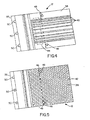
- the flat flexible circuit includes an elongated flat flexible dielectric substrate 38 having laterally spaced strips of signal conductors 40 on one side thereof as best seen in Figures 4 and 6 .
- a grounding conductor (or conductors) is disposed on the opposite side of substrate 38 in the form of a grounding grid 42 as shown in Figures 5 and 7 .
- the grounding grid is effective to provide a shielding means for the flat flexible circuit.
- the signal conductors and the grounding grid are covered with a thin flexible projective layer of dielectric material.
- the film is cut-out at least in the area of rectangular dotted lines 44 ( Figs. 4 and 6 ) to expose signal conductors 40 along the top of yieldable backing rib 36 so that the conductors can be biased into engagement with the conductors of the complementary mating connecting device.
- the dielectric film which covers grounding grid 42 is cut-out, at least in the areas indicated by dotted circles 46 ( Figs. 5 and 7 ), around a pair of locating holes 48.
- three locating holes 50 are formed through the circuit near a leading edge 52 thereof.
- Figures 4 and 5 show the flexible circuit in a flat condition
- Figures 6 and 7 show the circuit as it would be wrapped about leading edge 22 of body member 24 of male connector 16.
- Figure 8 shows double-sided flat flexible circuit 12 threaded through slot 30 beneath flange 28 of male connector 16 as is seen in Figure 1 .
- arrows 54 indicate the signal conductor side ( Figs. 4 and 6 ) of the circuit
- arrows 56 indicate the shielded or grounding grid side ( Figs. 5 and 7 ) of the circuit. Therefore, when the circuit is mounted within male connector 16 and wrapped around leading edge 22 thereof, yieldable backing rib 36 is effective to bias the signal conductors away from body member 24 in the direction of arrow "C" ( Fig. 8 ).
- Locating pegs 34 at the bottom of the male connector extend through locating holes 50 of the flexible circuit in an area where there are neither signal conductors nor grounding conductors. Therefore, locating pegs 34 are effective to anchor the leading edge of the flat flexible circuit.
- grounding grid is commoned to conductive connector body member 24 which, in turn, can be used for engaging grounding or shielding means on whatever type of receptacle device with which the male connector is mated.
- the substrate of flat flexible circuit 12 may be less than 0.050 inch thick, with each locating hole 48 being generally round and of a given diameter.
- the cross-dimensions of locating pegs 32 are greater than the diameters of round holes 48.
- the difference between the cross-dimensions of locating pegs 32 and the diameters of the round locating holes 48 is on the order of 5% to 50% of the diameters of the holes.
- Figures 9 and 10 show an alternative embodiment of a male connector, generally designated 16A which includes a male body member 24 about which a "single-sided" flat flexible circuit 14 is wrapped.
- the single-sided circuit has what can be termed an "active side” as indicated by arrows 62 in Figure 9 .
- Figure 10 shows the single-sided flat flexible circuit 14 to include signal conductors 40 and a pair of grounding grids 42 which only cover edge areas of substrate 38 outside the elongated signal conductors.
- single-sided circuit 14 includes a pair of locating holes 48 which extend through grounding grids 42 and three locating holes 50 along the leading edge 52 of the circuit.
- male connector 16A also includes a resilient backing rib 36 which biases signal conductors 40 away from male body member 24 in the direction of arrow "C".
- Figure 9 also shows locating pegs 34 of the connector extending through locating holes 50 of the circuit.
- connector 16A in Figure 9 has a pair of locating pegs 64 which project in a direction opposite locating pegs 32 of connector 16. This can be seen easily by comparing Figures 8 and 9 .
- locating pegs 64 project through locating holes 48 in grounding grids 42 ( Fig. 10 )
- locating pegs 64 are effective to common the grounding grids with the conductive connector body member.
- locating pegs 64 and locating holes 48 are dimensioned to take advantage of the "controlled meniscus" principle.
Landscapes
- Details Of Connecting Devices For Male And Female Coupling (AREA)
- Coupling Device And Connection With Printed Circuit (AREA)
- Multi-Conductor Connections (AREA)
Claims (11)
- Verbindersystem zum elektrischen Verbinden der Leiter (40, 42) einer geschirmten, flachen, flexiblen Schaltung (12, 14) mit den Leitern einer komplementär zu paarenden Verbindungseinrichtung (18), dadurch gekennzeichnet, dass dieses umfasst:ein Verbinderkorpuselement (24) zum Anordnen der flachen, flexiblen Schaltung auf diesem, wobei das Korpuselement leitfähig ist und mindestens einen Vorsprung (32, 34; 32, 64) aufweist; undeine flache, flexible Schaltung (12, 14) zum Anordnen an dem Korpuselement, wobei diese eine Mehrzahl von Signalleitern (40) und mindestens einen Erdungsleiter (42) umfasst, wobei sich in der Schaltung ein Loch (48, 50) befindet, und zwar zur Aufnahme des Vorsprungs in Anlage an dem Erdungsleiter und dadurch zum Verbinden des Erdungsleiters (42) mit dem leitfähigen Verbinderkorpuselement (24).
- Verbindersystem zum elektrischen Verbinden der Leiter (40, 42) einer geschirmten, flachen, flexiblen Schaltung (14) mit den Leitern einer komplementär zu paarenden Verbindungseinrichtung (18), dadurch gekennzeichnet, dass dieses umfasst:ein Verbinderkorpuselement (24) zum Anordnen der flachen, flexiblen Schaltung (14) auf diesem, wobei das Korpuselement leitfähig ist;eine flache, flexible Schaltung (14), die auf dem Korpuselement (24) angeordnet werden kann und die eine Mehrzahl von Signalleitern (40) und mindestens einen Erdungsleiter (42) umfasst, die sich alle auf derselben Seite der Schaltung befinden, wobei die Signalleiter (40) von dem Korpuselement abgewandt sind, um an den Leitern der komplementär zu paarenden Verbindungseinrichtung in Anlage zu kommen, sowie ein Loch (48) in der Schaltung in der Nähe des Erdungsleiters (42); undeinen Vorsprung (64) an dem Verbinderkorpuselement (24) in Entfernung zu den Signalleitern (40) zum Hindurchragen durch das Loch (48) und zum In-Anlage-Kommen an dem Erdungsleiter (42) und dadurch zum Verbinden des Erdungsleiters (42) mit dem leitfähigen Verbinderkorpuselement (24).
- Verbindersystem nach Anspruch 1, wobei die flache, flexible Schaltung (12) ein flexibles, isolierendes Substrat (38) umfasst, wobei sich die Signalleiter (40) auf mindestens einer Seite des Substrates erstrecken und sich der Erdungsleiter (42) auf der entgegengesetzten Seite des Substrates erstreckt.
- Verbindersystem nach Anspruch 3, wobei sich der mindestens eine Vorsprung (32) von dem Korpuselement weg erstreckt;
wobei das flexible, isolierende Substrat (38) flach ist, wobei die mehreren Signalleiter (40) auf einer von dem Korpuselement abgewandten Seite des Substrates angeordnet sind, und wobei der mindestens eine Erdungsleiter (42) auf einer entgegengesetzten Seite des Substrates angeordnet ist, die dem Korpus zugewandt ist. - Verbindersystem nach Anspruch 1 oder 4, wobei das Verbinderkorpuselement ein einzufügendes Korpuselement (24) ist, um welches die flache, flexible Schaltung (12, 14) in solcher Weise herumgelegt wird, dass die Signalleiter (40) von dem Korpuselement abgewandt sind.
- Verbindersystem nach einem der Ansprüche 1, 2, 3 oder 4, wobei der Erdungsleiter ein Erdungsgitter (42) umfasst.
- Verbindersystem nach einem der Ansprüche 1, 2 oder 4, wobei das Loch (48) in der flachen, flexiblen Schaltung (12, 14) allgemein rund ist, wobei der Querschnitt des Vorsprungs (32, 64) größer ist als der Durchmesser des Loches, und wobei die Differenz zwischen dem Querschnitt des Vorsprungs (32, 64) und dem Durchmesser des Loches (48) in der Größenordnung von 5 % bis 50 % des Durchmessers des Loches liegt.
- Verbindersystem nach einem der Ansprüche 1, 2 oder 4, wobei die flache, flexible Schaltung (12, 14) in solcher Weise auf dem Korpuselement (24) angeordnet werden kann, dass die Signalleiter (40) von dem Korpuselement abgewandt sind, und wobei dieses eine nachgiebige Hinterstützungsstruktur (36) an dem Korpuselement unter der flexiblen Schaltung zum elastischen Drücken der Signalleiter nach außen aufweist.
- Verbindersystem nach Anspruch 8, wobei die nachgiebige Hinterstützungsstruktur (36) eine an Ort und Stelle angeformte Komponente darstellt.
- Verbindersystem nach Anspruch 9, wobei die an Ort und Stelle angeformte Komponente (36) aus einem elastomeren Material hergestellt ist.
- Verbindersystem nach Anspruch 10, wobei die an Ort und Stelle angeformte Komponente (36) aus Silikongummimaterial hergestellt ist.
Applications Claiming Priority (2)
| Application Number | Priority Date | Filing Date | Title |
|---|---|---|---|
| US09/112,081 US6010359A (en) | 1998-07-08 | 1998-07-08 | Electrical connector system for shielded flat flexible circuitry |
| US112081 | 1998-07-08 |
Publications (3)
| Publication Number | Publication Date |
|---|---|
| EP0971443A2 EP0971443A2 (de) | 2000-01-12 |
| EP0971443A3 EP0971443A3 (de) | 2000-12-20 |
| EP0971443B1 true EP0971443B1 (de) | 2010-09-01 |
Family
ID=22342019
Family Applications (1)
| Application Number | Title | Priority Date | Filing Date |
|---|---|---|---|
| EP99112386A Expired - Lifetime EP0971443B1 (de) | 1998-07-08 | 1999-06-29 | Elektrisches Steckverbindungssystem für abgeschirmte flexible Flachchaltungen |
Country Status (7)
| Country | Link |
|---|---|
| US (1) | US6010359A (de) |
| EP (1) | EP0971443B1 (de) |
| JP (1) | JP3049610B2 (de) |
| KR (1) | KR100339972B1 (de) |
| CN (1) | CN1143411C (de) |
| BR (1) | BR9902659A (de) |
| DE (1) | DE69942713D1 (de) |
Families Citing this family (40)
| Publication number | Priority date | Publication date | Assignee | Title |
|---|---|---|---|---|
| DE4329898A1 (de) | 1993-09-04 | 1995-04-06 | Marcus Dr Besson | Kabelloses medizinisches Diagnose- und Überwachungsgerät |
| FR2805668A1 (fr) * | 2000-02-29 | 2001-08-31 | Siemens Automotive Sa | Connecteur par contact pour connecter un cable plat a un circuit imprime |
| US6533588B1 (en) * | 2000-03-30 | 2003-03-18 | Delphi Technologies, Inc. | Connector assembly for flexible circuits |
| US6496705B1 (en) * | 2000-04-18 | 2002-12-17 | Motorola Inc. | Programmable wireless electrode system for medical monitoring |
| US6441747B1 (en) * | 2000-04-18 | 2002-08-27 | Motorola, Inc. | Wireless system protocol for telemetry monitoring |
| EP1170825B1 (de) * | 2000-07-04 | 2004-10-06 | Autonetworks Technologies, Ltd. | Verbinder |
| US6611705B2 (en) * | 2000-07-18 | 2003-08-26 | Motorola, Inc. | Wireless electrocardiograph system and method |
| JP3380539B2 (ja) * | 2000-10-13 | 2003-02-24 | 山一電機株式会社 | フラットケーブル用コネクタ |
| US6688911B2 (en) * | 2000-12-13 | 2004-02-10 | Molex Incorporated | Electrical connector assembly for flat flexible circuitry |
| JP2003022855A (ja) * | 2001-07-09 | 2003-01-24 | Yazaki Corp | ホルダ |
| US7197357B2 (en) | 2001-07-17 | 2007-03-27 | Life Sync Corporation | Wireless ECG system |
| US7933642B2 (en) * | 2001-07-17 | 2011-04-26 | Rud Istvan | Wireless ECG system |
| US7446261B2 (en) | 2001-09-06 | 2008-11-04 | Finisar Corporation | Flexible circuit boards with tooling cutouts for optoelectronic modules |
| US7439449B1 (en) | 2002-02-14 | 2008-10-21 | Finisar Corporation | Flexible circuit for establishing electrical connectivity with optical subassembly |
| JP2003100392A (ja) * | 2001-09-25 | 2003-04-04 | Kyocera Elco Corp | Fpc/ffc用フローティングコネクタ |
| JP4082571B2 (ja) * | 2002-06-26 | 2008-04-30 | 矢崎総業株式会社 | コネクタの嵌脱構造 |
| JP4223771B2 (ja) * | 2002-09-02 | 2009-02-12 | 日本圧着端子製造株式会社 | 逆嵌合防止コネクタ |
| US7526207B2 (en) * | 2002-10-18 | 2009-04-28 | Finisar Corporation | Flexible circuit design for improved laser bias connections to optical subassemblies |
| DE10250924A1 (de) | 2002-10-31 | 2004-05-19 | Fci | Inline-Klemmverbinder für Flex-Flachbandkabel |
| DE10250933B3 (de) * | 2002-10-31 | 2004-08-12 | Fci | Verbinderanordnung zwischen einem Flex-Flachbandkabel und einer elektrischen Leiterplatte |
| TWM249444U (en) * | 2002-12-17 | 2004-11-01 | Hon Hai Prec Ind Co Ltd | Anti-EMI mechanism |
| DE602004001350T2 (de) * | 2003-01-16 | 2007-06-14 | Tyco Electronics Amp Gmbh | Stecker für Bandkabel |
| JP4408343B2 (ja) * | 2003-04-30 | 2010-02-03 | 日本圧着端子製造株式会社 | 多層プリント配線板の接続構造 |
| US20040224555A1 (en) * | 2003-05-08 | 2004-11-11 | Visteon Global Technologies, Inc. | Automotive flatwire connector |
| US6824969B1 (en) | 2004-03-09 | 2004-11-30 | Hon Hai Precision Ind. Co., Ltd | Low profile electrical assembly |
| US7425135B2 (en) * | 2004-04-30 | 2008-09-16 | Finisar Corporation | Flex circuit assembly |
| US7629537B2 (en) | 2004-07-09 | 2009-12-08 | Finisar Corporation | Single layer flex circuit |
| JP4291800B2 (ja) * | 2005-06-21 | 2009-07-08 | 日本圧着端子製造株式会社 | 電気的接続装置及びコネクタ |
| JP4818833B2 (ja) * | 2006-06-30 | 2011-11-16 | 日本圧着端子製造株式会社 | 平形柔軟ケーブルのハーネス |
| DE102007045510B4 (de) * | 2007-09-24 | 2025-05-15 | Schaeffler Technologies AG & Co. KG | Bauteil mit einer flexiblen Kontaktfolie |
| US8393918B2 (en) * | 2008-06-11 | 2013-03-12 | Pulse Electronics, Inc. | Miniaturized connectors and methods |
| JP5800597B2 (ja) * | 2011-06-24 | 2015-10-28 | 矢崎総業株式会社 | フラット回路体組付け構造 |
| JP5800598B2 (ja) * | 2011-06-24 | 2015-10-28 | 矢崎総業株式会社 | フラット回路体組付け構造 |
| US8840415B2 (en) * | 2011-10-05 | 2014-09-23 | Tyco Electronics Corporation | Power cable connector |
| CN102393137B (zh) * | 2011-11-03 | 2013-07-03 | 云南新立有色金属有限公司 | 一种直流密闭电弧炉连续冶炼钛渣精确给料的方法及装置 |
| CN103390809B (zh) * | 2012-05-07 | 2015-09-02 | 林雅萍 | 电连接器 |
| JP6074711B2 (ja) * | 2013-09-10 | 2017-02-08 | パナソニックIpマネジメント株式会社 | ケーブル保持部材、電気的接続装置、コネクタ装置 |
| US9509098B1 (en) * | 2015-11-18 | 2016-11-29 | Tyco Electronics Corporation | Pluggable connector having bussed ground conductors |
| WO2020241347A1 (ja) | 2019-05-24 | 2020-12-03 | 株式会社村田製作所 | コネクタ構造及びコネクタ |
| JP7094641B2 (ja) * | 2019-10-16 | 2022-07-04 | 矢崎総業株式会社 | コネクタ |
Family Cites Families (14)
| Publication number | Priority date | Publication date | Assignee | Title |
|---|---|---|---|---|
| US3602870A (en) * | 1969-04-30 | 1971-08-31 | Westinghouse Electric Corp | Connector apparatus for effecting electrical connections |
| GB1317264A (en) * | 1970-03-23 | 1973-05-16 | Cannon Electric Great Britain | Electrical connectors |
| US3904261A (en) * | 1971-05-10 | 1975-09-09 | Ncr Co | Electrical cable connector |
| US3825878A (en) * | 1973-09-10 | 1974-07-23 | Motorola Inc | Flexible flat cable system |
| US4420201A (en) * | 1981-11-09 | 1983-12-13 | Amp Incorporated | Shielding assembly enclosing an electrical connector terminating shielded cable |
| US4802866A (en) * | 1987-08-10 | 1989-02-07 | Alfiero Balzano | Connector |
| US5383788A (en) * | 1993-05-20 | 1995-01-24 | W. L. Gore & Associates, Inc. | Electrical interconnect assembly |
| DE4341104C1 (de) * | 1993-12-02 | 1995-01-12 | Harting Elektronik Gmbh | Abgeschirmte Leiterplattensteckverbindung |
| US5384435A (en) * | 1994-01-28 | 1995-01-24 | Molex Incorporated | Mounting terminal pins in substrates |
| US5529502A (en) * | 1994-06-01 | 1996-06-25 | Motorola, Inc. | Solderless flexible circuit carrier to printed circuit board interconnection |
| US5556300A (en) * | 1994-11-14 | 1996-09-17 | The Whitaker Corporation | End connection for a flexible shielded cable conductor |
| WO1996023331A1 (en) * | 1995-01-23 | 1996-08-01 | The Whitaker Corporation | Electrical connector assembly |
| JP3083982B2 (ja) * | 1995-08-18 | 2000-09-04 | トーマス アンド ベッツ コーポレーション | ケーブルアセンブリ |
| US5752851A (en) * | 1996-02-05 | 1998-05-19 | Ford Motor Company | Circuit clip connector |
-
1998
- 1998-07-08 US US09/112,081 patent/US6010359A/en not_active Expired - Lifetime
-
1999
- 1999-06-29 EP EP99112386A patent/EP0971443B1/de not_active Expired - Lifetime
- 1999-06-29 DE DE69942713T patent/DE69942713D1/de not_active Expired - Lifetime
- 1999-07-06 JP JP11191248A patent/JP3049610B2/ja not_active Expired - Fee Related
- 1999-07-07 CN CNB991101936A patent/CN1143411C/zh not_active Expired - Fee Related
- 1999-07-07 BR BR9902659-7A patent/BR9902659A/pt not_active Application Discontinuation
- 1999-07-08 KR KR1019990027631A patent/KR100339972B1/ko not_active Expired - Fee Related
Also Published As
| Publication number | Publication date |
|---|---|
| EP0971443A2 (de) | 2000-01-12 |
| CN1241047A (zh) | 2000-01-12 |
| KR20000011586A (ko) | 2000-02-25 |
| JP2000036340A (ja) | 2000-02-02 |
| DE69942713D1 (de) | 2010-10-14 |
| EP0971443A3 (de) | 2000-12-20 |
| CN1143411C (zh) | 2004-03-24 |
| US6010359A (en) | 2000-01-04 |
| KR100339972B1 (ko) | 2002-06-10 |
| BR9902659A (pt) | 2000-01-18 |
| JP3049610B2 (ja) | 2000-06-05 |
Similar Documents
| Publication | Publication Date | Title |
|---|---|---|
| EP0971443B1 (de) | Elektrisches Steckverbindungssystem für abgeschirmte flexible Flachchaltungen | |
| EP0578888B1 (de) | Datenkarten-Umkreisschirm | |
| EP0188876B1 (de) | Anordnung für einen abgeschirmten elektrischen Verbinder | |
| EP0073957B1 (de) | Abgeschirmter elektrischer Verbinder | |
| US6780030B2 (en) | Information processing equipment | |
| KR970004154B1 (ko) | 차폐 모듈 잭 | |
| US7892007B2 (en) | Electrical connector assembly | |
| US5647765A (en) | Shielded connector with conductive gasket interface | |
| US5281169A (en) | Shielded electrical connector assemblies | |
| US20020142636A1 (en) | Electrical connector assembly utilizing multiple ground planes | |
| JPH02195675A (ja) | 低プロファイルシールドジャッキ | |
| US4732568A (en) | Electrical connector with integral ground strap for shielded cable | |
| WO2006026036A1 (en) | Flat circuit connector | |
| KR19980032754A (ko) | 전기 접지 시라우드 | |
| US6264504B1 (en) | Electrical connector | |
| US6361332B1 (en) | Retention system for electrical connectors | |
| GB2227131A (en) | Shielded electrical connectors | |
| KR19990072230A (ko) | Esd 보호형 전기 커넥터 | |
| US5330365A (en) | Adapter unit with flexible carrier | |
| US4738638A (en) | Electrical connector with improved integral ground strap for shielded cable | |
| MY127073A (en) | Circuit board straddle mounted connector | |
| US6994591B2 (en) | Electrical connector for use with flexible printed circuit | |
| US6210228B1 (en) | Shielded electrical connector | |
| JP2948914B2 (ja) | 電気コネクタと印刷回路板 | |
| US5967806A (en) | Electrical connector arrangement |
Legal Events
| Date | Code | Title | Description |
|---|---|---|---|
| PUAI | Public reference made under article 153(3) epc to a published international application that has entered the european phase |
Free format text: ORIGINAL CODE: 0009012 |
|
| AK | Designated contracting states |
Kind code of ref document: A2 Designated state(s): DE FR GB IT |
|
| AX | Request for extension of the european patent |
Free format text: AL;LT;LV;MK;RO;SI |
|
| PUAL | Search report despatched |
Free format text: ORIGINAL CODE: 0009013 |
|
| AK | Designated contracting states |
Kind code of ref document: A3 Designated state(s): AT BE CH CY DE DK ES FI FR GB GR IE IT LI LU MC NL PT SE |
|
| AX | Request for extension of the european patent |
Free format text: AL;LT;LV;MK;RO;SI |
|
| 17P | Request for examination filed |
Effective date: 20010612 |
|
| AKX | Designation fees paid |
Free format text: DE FR GB IT |
|
| 17Q | First examination report despatched |
Effective date: 20050322 |
|
| GRAP | Despatch of communication of intention to grant a patent |
Free format text: ORIGINAL CODE: EPIDOSNIGR1 |
|
| GRAS | Grant fee paid |
Free format text: ORIGINAL CODE: EPIDOSNIGR3 |
|
| GRAA | (expected) grant |
Free format text: ORIGINAL CODE: 0009210 |
|
| AK | Designated contracting states |
Kind code of ref document: B1 Designated state(s): DE FR GB IT |
|
| REG | Reference to a national code |
Ref country code: GB Ref legal event code: FG4D |
|
| REF | Corresponds to: |
Ref document number: 69942713 Country of ref document: DE Date of ref document: 20101014 Kind code of ref document: P |
|
| PG25 | Lapsed in a contracting state [announced via postgrant information from national office to epo] |
Ref country code: IT Free format text: LAPSE BECAUSE OF FAILURE TO SUBMIT A TRANSLATION OF THE DESCRIPTION OR TO PAY THE FEE WITHIN THE PRESCRIBED TIME-LIMIT Effective date: 20100901 |
|
| PLBE | No opposition filed within time limit |
Free format text: ORIGINAL CODE: 0009261 |
|
| STAA | Information on the status of an ep patent application or granted ep patent |
Free format text: STATUS: NO OPPOSITION FILED WITHIN TIME LIMIT |
|
| 26N | No opposition filed |
Effective date: 20110606 |
|
| REG | Reference to a national code |
Ref country code: DE Ref legal event code: R097 Ref document number: 69942713 Country of ref document: DE Effective date: 20110606 |
|
| GBPC | Gb: european patent ceased through non-payment of renewal fee |
Effective date: 20110629 |
|
| PG25 | Lapsed in a contracting state [announced via postgrant information from national office to epo] |
Ref country code: GB Free format text: LAPSE BECAUSE OF NON-PAYMENT OF DUE FEES Effective date: 20110629 |
|
| PGFP | Annual fee paid to national office [announced via postgrant information from national office to epo] |
Ref country code: DE Payment date: 20120627 Year of fee payment: 14 |
|
| PGFP | Annual fee paid to national office [announced via postgrant information from national office to epo] |
Ref country code: FR Payment date: 20120705 Year of fee payment: 14 |
|
| REG | Reference to a national code |
Ref country code: FR Ref legal event code: ST Effective date: 20140228 |
|
| PG25 | Lapsed in a contracting state [announced via postgrant information from national office to epo] |
Ref country code: DE Free format text: LAPSE BECAUSE OF NON-PAYMENT OF DUE FEES Effective date: 20140101 |
|
| PG25 | Lapsed in a contracting state [announced via postgrant information from national office to epo] |
Ref country code: FR Free format text: LAPSE BECAUSE OF NON-PAYMENT OF DUE FEES Effective date: 20130701 |
|
| REG | Reference to a national code |
Ref country code: DE Ref legal event code: R119 Ref document number: 69942713 Country of ref document: DE Effective date: 20140101 Ref country code: DE Ref legal event code: R079 Ref document number: 69942713 Country of ref document: DE Free format text: PREVIOUS MAIN CLASS: H01R0012080000 Ipc: H01R0012500000 Effective date: 20140508 |