EP0971459A2 - Connecteur de communication avec faible retard de diaphonie complémentaire - Google Patents
Connecteur de communication avec faible retard de diaphonie complémentaire Download PDFInfo
- Publication number
- EP0971459A2 EP0971459A2 EP99304911A EP99304911A EP0971459A2 EP 0971459 A2 EP0971459 A2 EP 0971459A2 EP 99304911 A EP99304911 A EP 99304911A EP 99304911 A EP99304911 A EP 99304911A EP 0971459 A2 EP0971459 A2 EP 0971459A2
- Authority
- EP
- European Patent Office
- Prior art keywords
- conductors
- carrier
- communication plug
- disposed
- conductor
- Prior art date
- Legal status (The legal status is an assumption and is not a legal conclusion. Google has not performed a legal analysis and makes no representation as to the accuracy of the status listed.)
- Granted
Links
- 238000004891 communication Methods 0.000 title claims abstract description 44
- 230000000295 complement effect Effects 0.000 title abstract description 19
- 239000004020 conductor Substances 0.000 claims abstract description 87
- 125000006850 spacer group Chemical group 0.000 claims description 8
- 238000009413 insulation Methods 0.000 claims description 3
- 238000006073 displacement reaction Methods 0.000 claims description 2
- 238000000926 separation method Methods 0.000 claims description 2
- 239000012141 concentrate Substances 0.000 claims 1
- 230000001939 inductive effect Effects 0.000 abstract description 11
- 238000013461 design Methods 0.000 description 6
- 230000001965 increasing effect Effects 0.000 description 4
- 238000012986 modification Methods 0.000 description 4
- 230000004048 modification Effects 0.000 description 4
- 239000003989 dielectric material Substances 0.000 description 3
- 230000005672 electromagnetic field Effects 0.000 description 3
- 239000000463 material Substances 0.000 description 3
- 230000008878 coupling Effects 0.000 description 2
- 238000010168 coupling process Methods 0.000 description 2
- 238000005859 coupling reaction Methods 0.000 description 2
- 230000009977 dual effect Effects 0.000 description 2
- 230000000694 effects Effects 0.000 description 2
- 238000000034 method Methods 0.000 description 2
- 239000000853 adhesive Substances 0.000 description 1
- 230000001070 adhesive effect Effects 0.000 description 1
- 239000002390 adhesive tape Substances 0.000 description 1
- 238000013459 approach Methods 0.000 description 1
- 230000005540 biological transmission Effects 0.000 description 1
- 239000003990 capacitor Substances 0.000 description 1
- 230000008859 change Effects 0.000 description 1
- 238000005520 cutting process Methods 0.000 description 1
- 230000001419 dependent effect Effects 0.000 description 1
- 238000012938 design process Methods 0.000 description 1
- 238000009826 distribution Methods 0.000 description 1
- 230000005670 electromagnetic radiation Effects 0.000 description 1
- 230000008030 elimination Effects 0.000 description 1
- 238000003379 elimination reaction Methods 0.000 description 1
- 230000002708 enhancing effect Effects 0.000 description 1
- 230000003993 interaction Effects 0.000 description 1
- 238000004519 manufacturing process Methods 0.000 description 1
- 230000013011 mating Effects 0.000 description 1
- 230000009467 reduction Effects 0.000 description 1
- 238000005204 segregation Methods 0.000 description 1
- 238000004804 winding Methods 0.000 description 1
Images
Classifications
-
- H—ELECTRICITY
- H01—ELECTRIC ELEMENTS
- H01R—ELECTRICALLY-CONDUCTIVE CONNECTIONS; STRUCTURAL ASSOCIATIONS OF A PLURALITY OF MUTUALLY-INSULATED ELECTRICAL CONNECTING ELEMENTS; COUPLING DEVICES; CURRENT COLLECTORS
- H01R13/00—Details of coupling devices of the kinds covered by groups H01R12/70 or H01R24/00 - H01R33/00
- H01R13/646—Details of coupling devices of the kinds covered by groups H01R12/70 or H01R24/00 - H01R33/00 specially adapted for high-frequency, e.g. structures providing an impedance match or phase match
- H01R13/6461—Means for preventing cross-talk
- H01R13/6464—Means for preventing cross-talk by adding capacitive elements
-
- H—ELECTRICITY
- H01—ELECTRIC ELEMENTS
- H01R—ELECTRICALLY-CONDUCTIVE CONNECTIONS; STRUCTURAL ASSOCIATIONS OF A PLURALITY OF MUTUALLY-INSULATED ELECTRICAL CONNECTING ELEMENTS; COUPLING DEVICES; CURRENT COLLECTORS
- H01R13/00—Details of coupling devices of the kinds covered by groups H01R12/70 or H01R24/00 - H01R33/00
- H01R13/646—Details of coupling devices of the kinds covered by groups H01R12/70 or H01R24/00 - H01R33/00 specially adapted for high-frequency, e.g. structures providing an impedance match or phase match
- H01R13/6473—Impedance matching
-
- H—ELECTRICITY
- H01—ELECTRIC ELEMENTS
- H01R—ELECTRICALLY-CONDUCTIVE CONNECTIONS; STRUCTURAL ASSOCIATIONS OF A PLURALITY OF MUTUALLY-INSULATED ELECTRICAL CONNECTING ELEMENTS; COUPLING DEVICES; CURRENT COLLECTORS
- H01R13/00—Details of coupling devices of the kinds covered by groups H01R12/70 or H01R24/00 - H01R33/00
- H01R13/66—Structural association with built-in electrical component
- H01R13/6608—Structural association with built-in electrical component with built-in single component
- H01R13/6625—Structural association with built-in electrical component with built-in single component with capacitive component
-
- H—ELECTRICITY
- H01—ELECTRIC ELEMENTS
- H01R—ELECTRICALLY-CONDUCTIVE CONNECTIONS; STRUCTURAL ASSOCIATIONS OF A PLURALITY OF MUTUALLY-INSULATED ELECTRICAL CONNECTING ELEMENTS; COUPLING DEVICES; CURRENT COLLECTORS
- H01R24/00—Two-part coupling devices, or either of their cooperating parts, characterised by their overall structure
- H01R24/60—Contacts spaced along planar side wall transverse to longitudinal axis of engagement
- H01R24/62—Sliding engagements with one side only, e.g. modular jack coupling devices
- H01R24/64—Sliding engagements with one side only, e.g. modular jack coupling devices for high frequency, e.g. RJ 45
-
- Y—GENERAL TAGGING OF NEW TECHNOLOGICAL DEVELOPMENTS; GENERAL TAGGING OF CROSS-SECTIONAL TECHNOLOGIES SPANNING OVER SEVERAL SECTIONS OF THE IPC; TECHNICAL SUBJECTS COVERED BY FORMER USPC CROSS-REFERENCE ART COLLECTIONS [XRACs] AND DIGESTS
- Y10—TECHNICAL SUBJECTS COVERED BY FORMER USPC
- Y10S—TECHNICAL SUBJECTS COVERED BY FORMER USPC CROSS-REFERENCE ART COLLECTIONS [XRACs] AND DIGESTS
- Y10S439/00—Electrical connectors
- Y10S439/941—Crosstalk suppression
Definitions
- the present invention relates generally to the field of modular communication plugs and, more particularly, to the generation of complementary crosstalk in a communication plug such that performance with connector jacks is optimized.
- Telecommunications and data transmission systems have evolved in recent years to accommodate the increasing demand for high speed, multi-media services. Accordingly, higher and higher frequencies are being transmitted across network infrastructure originally designed for lower throughput. Although present day cables and wiring, can, theoretically, handle such increased frequencies and traffic volume, the wiring paths themselves become, in effect, antennae that both radiate and receive electromagnetic radiation, thereby creating crosstalk problems. Crosstalk is particularly problematic in systems incorporating multiple wire pairs.
- the plugs and jacks that are most commonly used in interconnecting cables and hardware, such as distribution modules generally include up to eight wires (four wire pairs) that are necessarily oriented both parallel and close together, a condition that leads to excessive crosstalk, even over short distances, and which is exacerbated as the frequency of the signals or the data rate is increased.
- crosstalk signals generated in the plug and the jack or connector should be of equal magnitude and be 180° out of phase with one another.
- the crosstalk signals generated in the plug and the jack are separated initially by some defined distance, which results in a propagation time delay before the signals combine. This propagation delay can cause the phase difference between the two crosstalk signals to shift from the desired 180° to some other value, which prevents the plug and jack crosstalk signals from completely canceling one another out. It is therefore desirable, that the complementary crosstalk in the plug be generated proximal to the jack to minimize the propagation delay for the complementary crosstalk signals.
- a communication plug having engineerable parameters that can be modified to generate a desired level of crosstalk to adapt to the compensating crosstalk characteristics of a jack or connector in which the plug will be used.
- the communication plug Preferably, the communication plug generates the crosstalk near the plug-jack interface to minimize the propagation delay between the crosstalk signals from the respective components.
- the present invention is generally directed to a communication plug that generates crosstalk that complements the compensating crosstalk in a legacy jack or connector.
- the communication plug comprises a dielectric carrier on which a plurality of electrical conductors are disposed. Each conductor is configured to wrap around a first end of the carrier thereby forming a series of adjacent inductive loops. Crosstalk is generated between the conductors as a result of the fields created from current flow through the inductive loops.
- the complementary crosstalk generated in the plug can be fixed to a desired level by modifying certain engineerable parameters such as the direction that each conductor loops around the end of the carrier.
- Other engineerable parameters include the length of the inductive loops, the design of the dielectric carrier, and the type of material from which the carrier is made.
- the inductive loops are positioned in the nose or front region of the plug where the conductors engage the jack spring wires or terminals.
- the communication plug according to the present invention can optionally include means for complementing the impedance profile of a jack or connector.
- the impedance matching means comprises parallel plates disposed on certain conductors to create a capacitance within the plug.
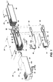
- a communication plug 20 embodying the principles of the present invention is shown to comprise a housing 22, a plurality of conductors 24, and a conductor carrier 26.
- Housing 22 which is typically made from a suitable dielectric material such as plastic, comprises a substantially hollow shell having side walls 28 and upper and lower walls 30a and 30b respectively.
- Upper wall 30a includes a plurality of slots 32 at the nose or front end of the housing for receiving jack springs contained in a wall terminal block or other connector containing a jack interface with which the plug of the invention is designed to mate.
- the number of slots 32 and the dimensions of housing 22 are dependent on the number of conductors to be terminated and/or connected and the shape of the jack in the terminal block. For most applications, the general shape of housing 22 remains consistent with the number of slots and the overall width thereof varies in relation to the number of conductors.
- housing 22 To secure communication plug 20 in a jack, housing 22 includes a resilient latch 34 extending from lower wall 30b. Because latch 34 is secured to housing 22 at only one end, leverage may be applied to the latch to raise or lower locking edges 36. When housing 22 is inserted into a jack, pressure can be applied to latch 34 to raise locking edges 36 for easy entry. Once housing 22 is seated within the jack, latch 34 can be released causing locking edges 36 to be held behind a plate forming the front of the jack, which is generally standard on such jacks, thereby securing the connection. Similarly, housing 22 can be released via leverage on latch 34 to free locking edges 36 from behind the jack plate so that housing 22 can be removed.
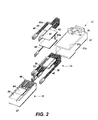
- the internal components of communication plug 20 include conductors 24 and conductor carrier 26.
- Carrier 26 is made from a dielectric material, such as plastic, and has channels and depressions formed thereon to receive the individual conductors 24.
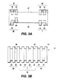
- the arrangement of conductors 24 once assembled in carrier 26 is shown best in FIGS. 3A and 3B.
- FIG. 3A depicts the IDC ends of conductors 24 extending from the rear or back end of carrier 26.
- FIG. 3B depicts the jack spring interface ends of conductors 24 arranged at the nose or front of carrier 26.
- the principles of the invention are disclosed as applied to an eight wire communication plug.
- pair I comprises conductors 44 and 46 (hereinafter pair 44-46); pair II comprises conductors 38 and 40 (hereinafter pair 38-40); pair III comprises conductors 42 and 48 (hereinafter pair 42-48); and pair IV comprises conductors 50 and 52 (hereinafter pair 50-52).
- pair numbering used herein is for example only. The principles of the present invention apply to any numbering scheme or pair assignment.
- Pairs 42-48 and 44-46 generally have the largest amount of crosstalk generated in plug 20 because the conductors in pair 42-48 must be split to straddle the conductors of pair 44-46 (see FIG. 2B), which is a common standard in eight conductor plugs.
- the crosstalk is generated not only between pairs 44-46 and 42-48, but between all pair combinations, and should be engineerable to complement the crosstalk generated in the jack or connector.
- communication plug 20 should have some means for fixing the amount of crosstalk generated between each pair combination.
- loop ends 54 are received in channels defined in the nose or front of carrier 26 by guide walls 58.
- IDC ends 56 rest at the rear or back end of carrier 26 with each contact being bifurcated to comprise dual, elongated prongs forming a narrow slot therebetween.
- the tips of the dual prongs are beveled to facilitate reception of an insulated wire from the cable and the inner edges of the prongs have sharp edges for cutting through the conductor insulation.
- Loop ends 54 are the primary means by which complementary crosstalk is engineered in communication plug 20.
- loop ends 54 are positioned close together such that a series or array of inductive loops is formed whereby electrical alternating current flow in one loop generates an electromagnetic field that triggers current flow in neighboring loops.
- the direction of the electromagnetic field and the direction of the current flow are related.
- loops 54 are located in substantially parallel planes with one another, which produces the greatest inductive interaction. Also, the proximity of the conductors in this region gives rise to capacitance between the conductors, which generates crosstalk.
- the first parameter is selection of which conductors run along the top 57 of carrier 26, and which run along the bottom 59.
- conductors 38, 40, 50, and 52 i.e., pairs II and IV
- conductors 44, 46, 42, and 48 i.e. pairs I and III
- the current runs along the top 57 of the carrier 26 only, and in conductors 44, 46, 22, and 48 the current runs along the bottom 59 of carrier 26 and up the front or nose of carrier 26 ( i.e., along length L 2 ).
- the electromagnetic field, and hence the inductively coupled crosstalk is directly related to the current flow in the conductor.
- the capacitive coupling is related to the proximity of the respective conductors to one another.
- One particular set of conductor locations is disclosed herein as a preferred embodiment. It should be understood that implementations using other sets of conductor locations in which crosstalk conduction is optimized as taught hereafter are within the spirit of the present invention.
- the length L 4 over which the inductive loops of pairs 44-46 and 42-48 are closely spaced can be adjusted. This has a direct effect on the amount of inductively coupled crosstalk and capacitively coupled crosstalk generated between pairs 44-46 and 42-48 in the loop 54 region ( i.e., along lengths L 1 , L 2 , and L 3 ) .
- the length L 5 of the non-current carrying extensions of all eight conductors can be varied independently to alter their capacitive coupling.
- a fourth parameter for managing crosstalk in communication plug 20 is the design of carrier 26 and the material from which carrier 26 is made. Carrier 26 is generally made from a dielectric material such as plastic, which increases capacitance, and hence crosstalk between conductor pairs.
- carrier 26 is generally designed to maximize the electrical segregation of conductors 24 in the region identified as L 6 in FIG. 1, which begins with the termination of loop ends 54 and extends to the IDC ends of conductors 24.
- the present invention generates complementary crosstalk in the communication plug predominantly along the region defined by lengths L 1 , L 2 , and L 3 through inductive loop ends 54, and through capacitive unbalance in this region.
- the complementary crosstalk is generated at the junction where communication plug 20 engages the jack springs of a jack or connector thus minimizing any signal propagation delay and facilitating the elimination of crosstalk in the system with proper compensation techniques.
- the mated combination of plug 20 and its jack is also required to meet certain return loss requirements as prescribed in standards set forth by the International Electrotechnical Commission (IEC) and Telecommunication Industry Association (TIA). These standards effectively place limits on the impedance of the plug. Furthermore, it is well known that to minimize return loss of a mating communication plug and a jack or connector, the impedance of the connection point should match that of the cabling it is used with. Accordingly, capacitive plates 60a and 60b are designed into conductors 48 and 42 respectively ( i.e., pair 42-48) to manage the impedance of the mated combination of the jack or connector and plug 20, and to comply with IEC and TIA standards.
- IEC International Electrotechnical Commission
- TIA Telecommunication Industry Association
- Dielectric spacer 62 which is typically made from plastic having a high dielectric constant, separates plates 60a and 60b to form a capacitor. Dielectric spacer 62 can be frictionally held between plates 60a and 60b and/or secured with an adhesive.
- the bottom 59 of carrier 26 includes a recessed region 64 for receiving plates 60a, 60b, and spacer 62.
- Other means can also be used for separating plates 60a and 60b. For example, it is common to use a dielectric adhesive tape on the underside of plate 60a to fulfill the role of spacer 62.
- the size of plates 60a and 60b, the size of dielectric spacer 62, and the type of material spacer 62 is made from can all be modified to adjust the capacitance level.
- plates 60a and 60b can alternatively be designed from discrete components and placed in proximity to the desired conductors with proper support from carrier 26.
- dielectric spacer 62 causes conductor 48 to be offset slightly from the remaining conductors in pairs 44-46 and 42-48 as shown in FIGS. 2 and 3A.
- alternative means can be used to adjust the impedance and capacitance developed in communication plug 20 such as alternative plate designs, routing the conductors close together to form capacitive regions, and designing resistive regions in conductors 24, which could change the spatial configuration of both conductors 24 and/or carrier 26.
- the principles of the present invention have been illustrated herein as embodied in a communication plug for a multi-wire cable. From the foregoing, it can readily be seen that the communication plug can be engineered during the design process to generate complementary crosstalk to match the characteristics of the jack or connector to which the plug will be mated. Most importantly, however, the complementary crosstalk is generated at the nose or front of the plug where the conductors engage the jack springs in the jack or connector thus minimizing any signal propagation delay and maximizing the effectiveness of the crosstalk compensation design. Several engineerable parameters are identified that can be adjusted during the design and manufacturing phases of the plug to fix the complementary crosstalk level.
Landscapes
- Details Of Connecting Devices For Male And Female Coupling (AREA)
- Coupling Device And Connection With Printed Circuit (AREA)
Applications Claiming Priority (2)
| Application Number | Priority Date | Filing Date | Title |
|---|---|---|---|
| US109125 | 1993-08-19 | ||
| US09/109,125 US6042427A (en) | 1998-06-30 | 1998-06-30 | Communication plug having low complementary crosstalk delay |
Publications (3)
| Publication Number | Publication Date |
|---|---|
| EP0971459A2 true EP0971459A2 (fr) | 2000-01-12 |
| EP0971459A3 EP0971459A3 (fr) | 2001-04-25 |
| EP0971459B1 EP0971459B1 (fr) | 2005-03-30 |
Family
ID=22325926
Family Applications (1)
| Application Number | Title | Priority Date | Filing Date |
|---|---|---|---|
| EP99304911A Expired - Lifetime EP0971459B1 (fr) | 1998-06-30 | 1999-06-23 | Connecteur de communication avec faible retard de diaphonie complémentaire |
Country Status (6)
| Country | Link |
|---|---|
| US (1) | US6042427A (fr) |
| EP (1) | EP0971459B1 (fr) |
| JP (1) | JP3776261B2 (fr) |
| AU (1) | AU756997B2 (fr) |
| CA (1) | CA2272012C (fr) |
| DE (1) | DE69924433T2 (fr) |
Cited By (6)
| Publication number | Priority date | Publication date | Assignee | Title |
|---|---|---|---|---|
| EP3152805A4 (fr) * | 2014-06-05 | 2017-11-22 | Bel Fuse (Macao Commercial Offshore) Limited | Connecteur d'interface de réseau à compensation de proximité |
| CN108886220A (zh) * | 2016-04-13 | 2018-11-23 | 泛达公司 | 在插头接口触点之间具有介电膜的通信插座 |
| US10424874B2 (en) | 2015-11-11 | 2019-09-24 | Bel Fuse (Macao Commerical Offshore) Limited | Modular jack connector with offset circuitry for controlled capacitance compensation |
| US10530106B2 (en) | 2018-01-31 | 2020-01-07 | Bel Fuse (Macao Commercial Offshore) Limited | Modular plug connector with multilayer PCB for very high speed applications |
| US10637196B2 (en) | 2015-11-11 | 2020-04-28 | Bel Fuse (Macao Commercial Offshore) Limited | Modular jack contact assembly having controlled capacitive coupling positioned within a jack housing |
| EP3683900A1 (fr) * | 2010-10-21 | 2020-07-22 | Panduit Corp. | Fiche rj45 comprenant un pcb flexible améliorant la diaphonie |
Families Citing this family (77)
| Publication number | Priority date | Publication date | Assignee | Title |
|---|---|---|---|---|
| US6283768B1 (en) * | 1999-05-13 | 2001-09-04 | Ideal Industries, Inc. | RJ-45 style modular connector |
| US6186834B1 (en) * | 1999-06-08 | 2001-02-13 | Avaya Technology Corp. | Enhanced communication connector assembly with crosstalk compensation |
| US6312292B2 (en) | 1999-06-09 | 2001-11-06 | Dan-Chief Enterprise Co. | Low crosstalk connector |
| TW482339U (en) * | 1999-06-09 | 2002-04-01 | Dan Chief Entpr Co Ltd | Low crosstalk connector |
| US6176742B1 (en) * | 1999-06-25 | 2001-01-23 | Avaya Inc. | Capacitive crosstalk compensation arrangement for communication connectors |
| US6165023A (en) * | 1999-10-28 | 2000-12-26 | Lucent Technologies Inc. | Capacitive crosstalk compensation arrangement for a communication connector |
| US6244907B1 (en) | 2000-08-02 | 2001-06-12 | Avaya Technology Corp. | Selectable compatibility electrical connector assembly |
| US6433272B1 (en) | 2000-09-19 | 2002-08-13 | Storage Technology Corporation | Crosstalk reduction in constrained wiring assemblies |
| DE10211603C1 (de) * | 2002-03-12 | 2003-10-02 | Ackermann Albert Gmbh Co | Elektrischer Steckverbinder für die Datentechnik |
| US6726503B2 (en) * | 2002-06-21 | 2004-04-27 | Molex Incorporated | Electrical connector with wire management module |
| US6964587B2 (en) * | 2002-11-10 | 2005-11-15 | Bel Fuse Ltd. | High performance, high capacitance gain, jack connector for data transmission or the like |
| US7265300B2 (en) * | 2003-03-21 | 2007-09-04 | Commscope Solutions Properties, Llc | Next high frequency improvement using hybrid substrates of two materials with different dielectric constant frequency slopes |
| US20050221678A1 (en) | 2004-02-20 | 2005-10-06 | Hammond Bernard Jr | Methods and systems for compensating for alien crosstalk between connectors |
| US7187766B2 (en) * | 2004-02-20 | 2007-03-06 | Adc Incorporated | Methods and systems for compensating for alien crosstalk between connectors |
| US10680385B2 (en) | 2004-02-20 | 2020-06-09 | Commscope Technologies Llc | Methods and systems for compensating for alien crosstalk between connectors |
| US7342181B2 (en) * | 2004-03-12 | 2008-03-11 | Commscope Inc. Of North Carolina | Maximizing capacitance per unit area while minimizing signal transmission delay in PCB |
| CA2464834A1 (fr) * | 2004-04-19 | 2005-10-19 | Nordx/Cdt Inc. | Connecteur |
| US7980900B2 (en) * | 2004-05-14 | 2011-07-19 | Commscope, Inc. Of North Carolina | Next high frequency improvement by using frequency dependent effective capacitance |
| US7190594B2 (en) * | 2004-05-14 | 2007-03-13 | Commscope Solutions Properties, Llc | Next high frequency improvement by using frequency dependent effective capacitance |
| US7281950B2 (en) * | 2004-09-29 | 2007-10-16 | Fci Americas Technology, Inc. | High speed connectors that minimize signal skew and crosstalk |
| US7186149B2 (en) * | 2004-12-06 | 2007-03-06 | Commscope Solutions Properties, Llc | Communications connector for imparting enhanced crosstalk compensation between conductors |
| US7326089B2 (en) * | 2004-12-07 | 2008-02-05 | Commscope, Inc. Of North Carolina | Communications jack with printed wiring board having self-coupling conductors |
| US7264516B2 (en) * | 2004-12-06 | 2007-09-04 | Commscope, Inc. | Communications jack with printed wiring board having paired coupling conductors |
| US7168993B2 (en) * | 2004-12-06 | 2007-01-30 | Commscope Solutions Properties Llc | Communications connector with floating wiring board for imparting crosstalk compensation between conductors |
| US7186148B2 (en) * | 2004-12-07 | 2007-03-06 | Commscope Solutions Properties, Llc | Communications connector for imparting crosstalk compensation between conductors |
| US7166000B2 (en) * | 2004-12-07 | 2007-01-23 | Commscope Solutions Properties, Llc | Communications connector with leadframe contact wires that compensate differential to common mode crosstalk |
| EP2224605B1 (fr) | 2004-12-07 | 2016-08-10 | Commscope Inc. of North Carolina | Connecteur commande de conversion de mode pour minimiser la diaphonie étrangère |
| WO2006062706A1 (fr) | 2004-12-07 | 2006-06-15 | Commscope Inc. Of North Carolina | Prise de telecommunication avec carte imprimee a conducteurs de couplage en paire |
| US7204722B2 (en) | 2004-12-07 | 2007-04-17 | Commscope Solutions Properties, Llc | Communications jack with compensation for differential to differential and differential to common mode crosstalk |
| US7220149B2 (en) * | 2004-12-07 | 2007-05-22 | Commscope Solutions Properties, Llc | Communication plug with balanced wiring to reduce differential to common mode crosstalk |
| US7320624B2 (en) * | 2004-12-16 | 2008-01-22 | Commscope, Inc. Of North Carolina | Communications jacks with compensation for differential to differential and differential to common mode crosstalk |
| EP1842296A1 (fr) * | 2005-01-28 | 2007-10-10 | Commscope Inc. of North Carolina | Connecteur commande de conversion de mode pour diminution d'intermodulation exterieure |
| US20060228912A1 (en) * | 2005-04-07 | 2006-10-12 | Fci Americas Technology, Inc. | Orthogonal backplane connector |
| US7314393B2 (en) * | 2005-05-27 | 2008-01-01 | Commscope, Inc. Of North Carolina | Communications connectors with floating wiring board for imparting crosstalk compensation between conductors |
| US7381098B2 (en) | 2006-04-11 | 2008-06-03 | Adc Telecommunications, Inc. | Telecommunications jack with crosstalk multi-zone crosstalk compensation and method for designing |
| US7407417B2 (en) * | 2006-04-26 | 2008-08-05 | Tyco Electronics Corporation | Electrical connector having contact plates |
| US7500871B2 (en) * | 2006-08-21 | 2009-03-10 | Fci Americas Technology, Inc. | Electrical connector system with jogged contact tails |
| JP4752699B2 (ja) * | 2006-09-21 | 2011-08-17 | パナソニック電工株式会社 | モジュラプラグ |
| US7497736B2 (en) * | 2006-12-19 | 2009-03-03 | Fci Americas Technology, Inc. | Shieldless, high-speed, low-cross-talk electrical connector |
| US7422444B1 (en) * | 2007-02-28 | 2008-09-09 | Fci Americas Technology, Inc. | Orthogonal header |
| AU2007201107B2 (en) * | 2007-03-14 | 2011-06-23 | Tyco Electronics Services Gmbh | Electrical Connector |
| AU2007201113B2 (en) * | 2007-03-14 | 2011-09-08 | Tyco Electronics Services Gmbh | Electrical Connector |
| AU2007201109B2 (en) * | 2007-03-14 | 2010-11-04 | Tyco Electronics Services Gmbh | Electrical Connector |
| AU2007201114B2 (en) * | 2007-03-14 | 2011-04-07 | Tyco Electronics Services Gmbh | Electrical Connector |
| AU2007201102B2 (en) | 2007-03-14 | 2010-11-04 | Tyco Electronics Services Gmbh | Electrical Connector |
| AU2007201108B2 (en) * | 2007-03-14 | 2012-02-09 | Tyco Electronics Services Gmbh | Electrical Connector |
| AU2007201106B9 (en) * | 2007-03-14 | 2011-06-02 | Tyco Electronics Services Gmbh | Electrical Connector |
| AU2007201105B2 (en) * | 2007-03-14 | 2011-08-04 | Tyco Electronics Services Gmbh | Electrical Connector |
| US7811100B2 (en) * | 2007-07-13 | 2010-10-12 | Fci Americas Technology, Inc. | Electrical connector system having a continuous ground at the mating interface thereof |
| US7857635B2 (en) * | 2007-09-12 | 2010-12-28 | Commscope, Inc. Of North Carolina | Board edge termination back-end connection assemblies and communications connectors including such assemblies |
| US7841909B2 (en) | 2008-02-12 | 2010-11-30 | Adc Gmbh | Multistage capacitive far end crosstalk compensation arrangement |
| US8764464B2 (en) * | 2008-02-29 | 2014-07-01 | Fci Americas Technology Llc | Cross talk reduction for high speed electrical connectors |
| US8545240B2 (en) | 2008-11-14 | 2013-10-01 | Molex Incorporated | Connector with terminals forming differential pairs |
| MY155071A (en) | 2008-12-12 | 2015-08-28 | Molex Inc | Resonance modifying connector |
| US8047879B2 (en) * | 2009-01-26 | 2011-11-01 | Commscope, Inc. Of North Carolina | Printed wiring boards and communication connectors having series inductor-capacitor crosstalk compensation circuits that share a common inductor |
| US8145442B2 (en) * | 2009-01-30 | 2012-03-27 | Synopsys, Inc. | Fast and accurate estimation of gate output loading |
| US9277649B2 (en) | 2009-02-26 | 2016-03-01 | Fci Americas Technology Llc | Cross talk reduction for high-speed electrical connectors |
| US8366485B2 (en) | 2009-03-19 | 2013-02-05 | Fci Americas Technology Llc | Electrical connector having ribbed ground plate |
| US8267721B2 (en) * | 2009-10-28 | 2012-09-18 | Fci Americas Technology Llc | Electrical connector having ground plates and ground coupling bar |
| US8616919B2 (en) * | 2009-11-13 | 2013-12-31 | Fci Americas Technology Llc | Attachment system for electrical connector |
| CN101800380B (zh) * | 2010-02-09 | 2012-05-23 | 永泰电子(东莞)有限公司 | 网络线插头、网络线插头对和网络线 |
| US7972183B1 (en) | 2010-03-19 | 2011-07-05 | Commscope, Inc. Of North Carolina | Sled that reduces the next variations between modular plugs |
| EP2624034A1 (fr) | 2012-01-31 | 2013-08-07 | Fci | Dispositif de couplage optique démontable |
| USD727852S1 (en) | 2012-04-13 | 2015-04-28 | Fci Americas Technology Llc | Ground shield for a right angle electrical connector |
| US8944831B2 (en) | 2012-04-13 | 2015-02-03 | Fci Americas Technology Llc | Electrical connector having ribbed ground plate with engagement members |
| USD727268S1 (en) | 2012-04-13 | 2015-04-21 | Fci Americas Technology Llc | Vertical electrical connector |
| US9257778B2 (en) | 2012-04-13 | 2016-02-09 | Fci Americas Technology | High speed electrical connector |
| USD718253S1 (en) | 2012-04-13 | 2014-11-25 | Fci Americas Technology Llc | Electrical cable connector |
| USD751507S1 (en) | 2012-07-11 | 2016-03-15 | Fci Americas Technology Llc | Electrical connector |
| US9543703B2 (en) | 2012-07-11 | 2017-01-10 | Fci Americas Technology Llc | Electrical connector with reduced stack height |
| US8764476B1 (en) | 2012-12-06 | 2014-07-01 | Frank Ma | Transmission connector |
| USD745852S1 (en) | 2013-01-25 | 2015-12-22 | Fci Americas Technology Llc | Electrical connector |
| USD720698S1 (en) | 2013-03-15 | 2015-01-06 | Fci Americas Technology Llc | Electrical cable connector |
| US9246274B2 (en) | 2013-03-15 | 2016-01-26 | Panduit Corp. | Communication connectors having crosstalk compensation networks |
| DE102013103069B3 (de) * | 2013-03-26 | 2014-06-26 | HARTING Electronics GmbH | Steckverbinder mit Übersprechkompensation |
| CN108390212B (zh) * | 2018-04-23 | 2024-01-12 | 孟祥君 | 一种高安全性能的霍尔感应插座 |
| CN115548735A (zh) * | 2022-09-23 | 2022-12-30 | 番禺得意精密电子工业有限公司 | 电连接器 |
Family Cites Families (12)
| Publication number | Priority date | Publication date | Assignee | Title |
|---|---|---|---|---|
| US716237A (en) * | 1902-04-14 | 1902-12-16 | Gustaf Alexander Johnson | Core-setter. |
| US766043A (en) * | 1903-11-14 | 1904-07-26 | Albert Lee Jones | Apparatus for destroying insects. |
| US4904209A (en) * | 1987-12-04 | 1990-02-27 | Amp Incorporated | Modular plug coupler |
| US5186647A (en) * | 1992-02-24 | 1993-02-16 | At&T Bell Laboratories | High frequency electrical connector |
| US5277625A (en) * | 1992-11-03 | 1994-01-11 | The Whitaker Corporation | Electrical connector with tape filter |
| GB2273397B (en) * | 1992-11-16 | 1997-01-29 | Krone Ag | Electrical connectors |
| US5470244A (en) * | 1993-10-05 | 1995-11-28 | Thomas & Betts Corporation | Electrical connector having reduced cross-talk |
| US5586914A (en) * | 1995-05-19 | 1996-12-24 | The Whitaker Corporation | Electrical connector and an associated method for compensating for crosstalk between a plurality of conductors |
| GB9511513D0 (en) * | 1995-06-07 | 1995-08-02 | Drewnicki Richard | Electrical connectors |
| US5766043A (en) * | 1996-02-29 | 1998-06-16 | Corcom, Inc. | Telephone connector |
| US5716237A (en) * | 1996-06-21 | 1998-02-10 | Lucent Technologies Inc. | Electrical connector with crosstalk compensation |
| US5911602A (en) * | 1996-07-23 | 1999-06-15 | Superior Modular Products Incorporated | Reduced cross talk electrical connector |
-
1998
- 1998-06-30 US US09/109,125 patent/US6042427A/en not_active Expired - Fee Related
-
1999
- 1999-05-11 CA CA002272012A patent/CA2272012C/fr not_active Expired - Fee Related
- 1999-06-23 DE DE69924433T patent/DE69924433T2/de not_active Expired - Fee Related
- 1999-06-23 EP EP99304911A patent/EP0971459B1/fr not_active Expired - Lifetime
- 1999-06-28 AU AU36821/99A patent/AU756997B2/en not_active Ceased
- 1999-06-30 JP JP18452299A patent/JP3776261B2/ja not_active Expired - Fee Related
Cited By (8)
| Publication number | Priority date | Publication date | Assignee | Title |
|---|---|---|---|---|
| EP3683900A1 (fr) * | 2010-10-21 | 2020-07-22 | Panduit Corp. | Fiche rj45 comprenant un pcb flexible améliorant la diaphonie |
| US11600960B2 (en) | 2010-10-21 | 2023-03-07 | Panduit Corp. | Communications plug with improved crosstalk |
| EP3152805A4 (fr) * | 2014-06-05 | 2017-11-22 | Bel Fuse (Macao Commercial Offshore) Limited | Connecteur d'interface de réseau à compensation de proximité |
| US10424874B2 (en) | 2015-11-11 | 2019-09-24 | Bel Fuse (Macao Commerical Offshore) Limited | Modular jack connector with offset circuitry for controlled capacitance compensation |
| US10637196B2 (en) | 2015-11-11 | 2020-04-28 | Bel Fuse (Macao Commercial Offshore) Limited | Modular jack contact assembly having controlled capacitive coupling positioned within a jack housing |
| CN108886220A (zh) * | 2016-04-13 | 2018-11-23 | 泛达公司 | 在插头接口触点之间具有介电膜的通信插座 |
| CN108886220B (zh) * | 2016-04-13 | 2021-06-25 | 泛达公司 | 在插头接口触点之间具有介电膜的通信插座 |
| US10530106B2 (en) | 2018-01-31 | 2020-01-07 | Bel Fuse (Macao Commercial Offshore) Limited | Modular plug connector with multilayer PCB for very high speed applications |
Also Published As
| Publication number | Publication date |
|---|---|
| EP0971459A3 (fr) | 2001-04-25 |
| EP0971459B1 (fr) | 2005-03-30 |
| AU3682199A (en) | 2000-01-13 |
| AU756997B2 (en) | 2003-01-30 |
| JP2000030813A (ja) | 2000-01-28 |
| DE69924433T2 (de) | 2006-02-23 |
| US6042427A (en) | 2000-03-28 |
| CA2272012A1 (fr) | 1999-12-30 |
| DE69924433D1 (de) | 2005-05-04 |
| JP3776261B2 (ja) | 2006-05-17 |
| CA2272012C (fr) | 2002-02-05 |
Similar Documents
| Publication | Publication Date | Title |
|---|---|---|
| US6042427A (en) | Communication plug having low complementary crosstalk delay | |
| US5967801A (en) | Modular plug having compensating insert | |
| US6007368A (en) | Telecommunications connector with improved crosstalk reduction | |
| CA2085270C (fr) | Connecteur electrique haute frequence | |
| EP0688473B1 (fr) | Connecteur electrique haute frequence ameliore | |
| CN100468883C (zh) | 模块化电缆端插头 | |
| US5586914A (en) | Electrical connector and an associated method for compensating for crosstalk between a plurality of conductors | |
| US5989071A (en) | Low crosstalk assembly structure for use in a communication plug | |
| EP1435679B1 (fr) | Connecteur électronique et méthode de réalisation d'une connexion électronique | |
| JP3446135B2 (ja) | モジュラージャックコネクタ | |
| CN101189763B (zh) | 具有屏蔽的差动触点对的电接插件 | |
| EP0899833B1 (fr) | Dispositif d'alignement pour un boítier de connecteur à Jack pour des connexions de télécommunications | |
| EP2122781A1 (fr) | Connecteur électrique | |
| JPH11144798A (ja) | 通信プラグ | |
| EP2122773A1 (fr) | Connecteur électrique | |
| US5791942A (en) | High frequency electrical connector | |
| AU769688B2 (en) | Communication plug having consistent and set levels of complementary crosstalk | |
| WO1999017406A1 (fr) | Fiche modulaire comportant une barre de charge pour la reduction de la diaphonie | |
| EP1881570B1 (fr) | Connecteur électronique et procédé pour effectuer une connexion électronique | |
| HK1115479B (en) | Electrical connector with shielded differential contact pairs |
Legal Events
| Date | Code | Title | Description |
|---|---|---|---|
| PUAI | Public reference made under article 153(3) epc to a published international application that has entered the european phase |
Free format text: ORIGINAL CODE: 0009012 |
|
| AK | Designated contracting states |
Kind code of ref document: A2 Designated state(s): DE FR GB |
|
| AX | Request for extension of the european patent |
Free format text: AL;LT;LV;MK;RO;SI |
|
| PUAL | Search report despatched |
Free format text: ORIGINAL CODE: 0009013 |
|
| AK | Designated contracting states |
Kind code of ref document: A3 Designated state(s): AT BE CH CY DE DK ES FI FR GB GR IE IT LI LU MC NL PT SE |
|
| AX | Request for extension of the european patent |
Free format text: AL;LT;LV;MK;RO;SI |
|
| RIC1 | Information provided on ipc code assigned before grant |
Free format text: 7H 01R 24/00 A, 7H 01R 23/02 B |
|
| 17P | Request for examination filed |
Effective date: 20011015 |
|
| AKX | Designation fees paid |
Free format text: DE FR GB |
|
| 17Q | First examination report despatched |
Effective date: 20031216 |
|
| GRAP | Despatch of communication of intention to grant a patent |
Free format text: ORIGINAL CODE: EPIDOSNIGR1 |
|
| GRAS | Grant fee paid |
Free format text: ORIGINAL CODE: EPIDOSNIGR3 |
|
| GRAA | (expected) grant |
Free format text: ORIGINAL CODE: 0009210 |
|
| RIC1 | Information provided on ipc code assigned before grant |
Ipc: 7H 01R 25/00 A |
|
| AK | Designated contracting states |
Kind code of ref document: B1 Designated state(s): DE FR GB |
|
| REG | Reference to a national code |
Ref country code: GB Ref legal event code: FG4D |
|
| REF | Corresponds to: |
Ref document number: 69924433 Country of ref document: DE Date of ref document: 20050504 Kind code of ref document: P |
|
| PLBE | No opposition filed within time limit |
Free format text: ORIGINAL CODE: 0009261 |
|
| STAA | Information on the status of an ep patent application or granted ep patent |
Free format text: STATUS: NO OPPOSITION FILED WITHIN TIME LIMIT |
|
| ET | Fr: translation filed | ||
| 26N | No opposition filed |
Effective date: 20060102 |
|
| PGFP | Annual fee paid to national office [announced via postgrant information from national office to epo] |
Ref country code: DE Payment date: 20090619 Year of fee payment: 11 |
|
| PGFP | Annual fee paid to national office [announced via postgrant information from national office to epo] |
Ref country code: FR Payment date: 20100630 Year of fee payment: 12 |
|
| PGFP | Annual fee paid to national office [announced via postgrant information from national office to epo] |
Ref country code: GB Payment date: 20100625 Year of fee payment: 12 |
|
| PG25 | Lapsed in a contracting state [announced via postgrant information from national office to epo] |
Ref country code: DE Free format text: LAPSE BECAUSE OF NON-PAYMENT OF DUE FEES Effective date: 20110101 |
|
| GBPC | Gb: european patent ceased through non-payment of renewal fee |
Effective date: 20110623 |
|
| REG | Reference to a national code |
Ref country code: FR Ref legal event code: ST Effective date: 20120229 |
|
| PG25 | Lapsed in a contracting state [announced via postgrant information from national office to epo] |
Ref country code: FR Free format text: LAPSE BECAUSE OF NON-PAYMENT OF DUE FEES Effective date: 20110630 |
|
| PG25 | Lapsed in a contracting state [announced via postgrant information from national office to epo] |
Ref country code: GB Free format text: LAPSE BECAUSE OF NON-PAYMENT OF DUE FEES Effective date: 20110623 |