EP0971463A2 - Laser à cavité annulaire - Google Patents
Laser à cavité annulaire Download PDFInfo
- Publication number
- EP0971463A2 EP0971463A2 EP99305470A EP99305470A EP0971463A2 EP 0971463 A2 EP0971463 A2 EP 0971463A2 EP 99305470 A EP99305470 A EP 99305470A EP 99305470 A EP99305470 A EP 99305470A EP 0971463 A2 EP0971463 A2 EP 0971463A2
- Authority
- EP
- European Patent Office
- Prior art keywords
- ring cavity
- face
- faces
- semiconductor
- laser according
- Prior art date
- Legal status (The legal status is an assumption and is not a legal conclusion. Google has not performed a legal analysis and makes no representation as to the accuracy of the status listed.)
- Withdrawn
Links
- 239000004065 semiconductor Substances 0.000 claims description 74
- 239000000758 substrate Substances 0.000 claims description 58
- 230000012010 growth Effects 0.000 claims description 50
- 238000000034 method Methods 0.000 claims description 37
- 238000005530 etching Methods 0.000 claims description 33
- 239000000463 material Substances 0.000 claims description 15
- 230000008569 process Effects 0.000 claims description 10
- 230000005855 radiation Effects 0.000 claims description 9
- WGPCGCOKHWGKJJ-UHFFFAOYSA-N sulfanylidenezinc Chemical compound [Zn]=S WGPCGCOKHWGKJJ-UHFFFAOYSA-N 0.000 claims 1
- 229910052984 zinc sulfide Inorganic materials 0.000 claims 1
- 239000010410 layer Substances 0.000 description 75
- VYPSYNLAJGMNEJ-UHFFFAOYSA-N Silicium dioxide Chemical compound O=[Si]=O VYPSYNLAJGMNEJ-UHFFFAOYSA-N 0.000 description 18
- 229910001218 Gallium arsenide Inorganic materials 0.000 description 15
- 238000004519 manufacturing process Methods 0.000 description 12
- 229910052681 coesite Inorganic materials 0.000 description 9
- 229910052906 cristobalite Inorganic materials 0.000 description 9
- 230000010355 oscillation Effects 0.000 description 9
- 230000010363 phase shift Effects 0.000 description 9
- 239000000377 silicon dioxide Substances 0.000 description 9
- 229910052682 stishovite Inorganic materials 0.000 description 9
- 229910052905 tridymite Inorganic materials 0.000 description 9
- 239000013078 crystal Substances 0.000 description 8
- 230000010287 polarization Effects 0.000 description 8
- 239000011159 matrix material Substances 0.000 description 7
- 230000003287 optical effect Effects 0.000 description 7
- QGZKDVFQNNGYKY-UHFFFAOYSA-N Ammonia Chemical compound N QGZKDVFQNNGYKY-UHFFFAOYSA-N 0.000 description 6
- KRHYYFGTRYWZRS-UHFFFAOYSA-N Fluorane Chemical compound F KRHYYFGTRYWZRS-UHFFFAOYSA-N 0.000 description 6
- PNEYBMLMFCGWSK-UHFFFAOYSA-N aluminium oxide Inorganic materials [O-2].[O-2].[O-2].[Al+3].[Al+3] PNEYBMLMFCGWSK-UHFFFAOYSA-N 0.000 description 6
- 229910052593 corundum Inorganic materials 0.000 description 6
- 230000008878 coupling Effects 0.000 description 6
- 238000010168 coupling process Methods 0.000 description 6
- 238000005859 coupling reaction Methods 0.000 description 6
- 229910001845 yogo sapphire Inorganic materials 0.000 description 6
- 239000007788 liquid Substances 0.000 description 5
- 238000002488 metal-organic chemical vapour deposition Methods 0.000 description 5
- 230000002269 spontaneous effect Effects 0.000 description 5
- 238000004544 sputter deposition Methods 0.000 description 5
- PCTMTFRHKVHKIS-BMFZQQSSSA-N (1s,3r,4e,6e,8e,10e,12e,14e,16e,18s,19r,20r,21s,25r,27r,30r,31r,33s,35r,37s,38r)-3-[(2r,3s,4s,5s,6r)-4-amino-3,5-dihydroxy-6-methyloxan-2-yl]oxy-19,25,27,30,31,33,35,37-octahydroxy-18,20,21-trimethyl-23-oxo-22,39-dioxabicyclo[33.3.1]nonatriaconta-4,6,8,10 Chemical compound C1C=C2C[C@@H](OS(O)(=O)=O)CC[C@]2(C)[C@@H]2[C@@H]1[C@@H]1CC[C@H]([C@H](C)CCCC(C)C)[C@@]1(C)CC2.O[C@H]1[C@@H](N)[C@H](O)[C@@H](C)O[C@H]1O[C@H]1/C=C/C=C/C=C/C=C/C=C/C=C/C=C/[C@H](C)[C@@H](O)[C@@H](C)[C@H](C)OC(=O)C[C@H](O)C[C@H](O)CC[C@@H](O)[C@H](O)C[C@H](O)C[C@](O)(C[C@H](O)[C@H]2C(O)=O)O[C@H]2C1 PCTMTFRHKVHKIS-BMFZQQSSSA-N 0.000 description 4
- 238000001312 dry etching Methods 0.000 description 4
- 238000002310 reflectometry Methods 0.000 description 4
- MHAJPDPJQMAIIY-UHFFFAOYSA-N Hydrogen peroxide Chemical class OO MHAJPDPJQMAIIY-UHFFFAOYSA-N 0.000 description 3
- 229910021529 ammonia Inorganic materials 0.000 description 3
- 238000005229 chemical vapour deposition Methods 0.000 description 3
- 230000005684 electric field Effects 0.000 description 3
- 239000002346 layers by function Substances 0.000 description 3
- 238000012545 processing Methods 0.000 description 3
- 230000001902 propagating effect Effects 0.000 description 3
- 238000005086 pumping Methods 0.000 description 3
- GWEVSGVZZGPLCZ-UHFFFAOYSA-N Titan oxide Chemical compound O=[Ti]=O GWEVSGVZZGPLCZ-UHFFFAOYSA-N 0.000 description 2
- 238000004891 communication Methods 0.000 description 2
- 150000001875 compounds Chemical class 0.000 description 2
- 239000011521 glass Substances 0.000 description 2
- 230000001965 increasing effect Effects 0.000 description 2
- 229910000679 solder Inorganic materials 0.000 description 2
- 229910017083 AlN Inorganic materials 0.000 description 1
- 229910000980 Aluminium gallium arsenide Inorganic materials 0.000 description 1
- 239000004642 Polyimide Substances 0.000 description 1
- 229910004205 SiNX Inorganic materials 0.000 description 1
- 238000013459 approach Methods 0.000 description 1
- 238000000149 argon plasma sintering Methods 0.000 description 1
- 238000003491 array Methods 0.000 description 1
- 230000005540 biological transmission Effects 0.000 description 1
- 238000006243 chemical reaction Methods 0.000 description 1
- 230000001276 controlling effect Effects 0.000 description 1
- 230000007423 decrease Effects 0.000 description 1
- 230000000694 effects Effects 0.000 description 1
- 230000002708 enhancing effect Effects 0.000 description 1
- 230000006872 improvement Effects 0.000 description 1
- 238000002347 injection Methods 0.000 description 1
- 239000007924 injection Substances 0.000 description 1
- 239000011810 insulating material Substances 0.000 description 1
- 230000010354 integration Effects 0.000 description 1
- CPLXHLVBOLITMK-UHFFFAOYSA-N magnesium oxide Inorganic materials [Mg]=O CPLXHLVBOLITMK-UHFFFAOYSA-N 0.000 description 1
- 230000007246 mechanism Effects 0.000 description 1
- 238000012986 modification Methods 0.000 description 1
- 230000004048 modification Effects 0.000 description 1
- 239000013307 optical fiber Substances 0.000 description 1
- 230000005693 optoelectronics Effects 0.000 description 1
- 239000011368 organic material Substances 0.000 description 1
- 238000000059 patterning Methods 0.000 description 1
- 230000002093 peripheral effect Effects 0.000 description 1
- 229920001721 polyimide Polymers 0.000 description 1
- 230000001105 regulatory effect Effects 0.000 description 1
- SBIBMFFZSBJNJF-UHFFFAOYSA-N selenium;zinc Chemical compound [Se]=[Zn] SBIBMFFZSBJNJF-UHFFFAOYSA-N 0.000 description 1
- 238000007493 shaping process Methods 0.000 description 1
- 238000007738 vacuum evaporation Methods 0.000 description 1
Images


Classifications
-
- H—ELECTRICITY
- H01—ELECTRIC ELEMENTS
- H01S—DEVICES USING THE PROCESS OF LIGHT AMPLIFICATION BY STIMULATED EMISSION OF RADIATION [LASER] TO AMPLIFY OR GENERATE LIGHT; DEVICES USING STIMULATED EMISSION OF ELECTROMAGNETIC RADIATION IN WAVE RANGES OTHER THAN OPTICAL
- H01S5/00—Semiconductor lasers
- H01S5/10—Construction or shape of the optical resonator, e.g. extended or external cavity, coupled cavities, bent-guide, varying width, thickness or composition of the active region
- H01S5/1071—Ring-lasers
-
- H—ELECTRICITY
- H01—ELECTRIC ELEMENTS
- H01S—DEVICES USING THE PROCESS OF LIGHT AMPLIFICATION BY STIMULATED EMISSION OF RADIATION [LASER] TO AMPLIFY OR GENERATE LIGHT; DEVICES USING STIMULATED EMISSION OF ELECTROMAGNETIC RADIATION IN WAVE RANGES OTHER THAN OPTICAL
- H01S2301/00—Functional characteristics
- H01S2301/14—Semiconductor lasers with special structural design for lasing in a specific polarisation mode
-
- H—ELECTRICITY
- H01—ELECTRIC ELEMENTS
- H01S—DEVICES USING THE PROCESS OF LIGHT AMPLIFICATION BY STIMULATED EMISSION OF RADIATION [LASER] TO AMPLIFY OR GENERATE LIGHT; DEVICES USING STIMULATED EMISSION OF ELECTROMAGNETIC RADIATION IN WAVE RANGES OTHER THAN OPTICAL
- H01S5/00—Semiconductor lasers
- H01S5/02—Structural details or components not essential to laser action
- H01S5/0206—Substrates, e.g. growth, shape, material, removal or bonding
- H01S5/0207—Substrates having a special shape
-
- H—ELECTRICITY
- H01—ELECTRIC ELEMENTS
- H01S—DEVICES USING THE PROCESS OF LIGHT AMPLIFICATION BY STIMULATED EMISSION OF RADIATION [LASER] TO AMPLIFY OR GENERATE LIGHT; DEVICES USING STIMULATED EMISSION OF ELECTROMAGNETIC RADIATION IN WAVE RANGES OTHER THAN OPTICAL
- H01S5/00—Semiconductor lasers
- H01S5/10—Construction or shape of the optical resonator, e.g. extended or external cavity, coupled cavities, bent-guide, varying width, thickness or composition of the active region
- H01S5/1042—Optical microcavities, e.g. cavity dimensions comparable to the wavelength
-
- H—ELECTRICITY
- H01—ELECTRIC ELEMENTS
- H01S—DEVICES USING THE PROCESS OF LIGHT AMPLIFICATION BY STIMULATED EMISSION OF RADIATION [LASER] TO AMPLIFY OR GENERATE LIGHT; DEVICES USING STIMULATED EMISSION OF ELECTROMAGNETIC RADIATION IN WAVE RANGES OTHER THAN OPTICAL
- H01S5/00—Semiconductor lasers
- H01S5/10—Construction or shape of the optical resonator, e.g. extended or external cavity, coupled cavities, bent-guide, varying width, thickness or composition of the active region
- H01S5/1082—Construction or shape of the optical resonator, e.g. extended or external cavity, coupled cavities, bent-guide, varying width, thickness or composition of the active region with a special facet structure, e.g. structured, non planar, oblique
-
- H—ELECTRICITY
- H01—ELECTRIC ELEMENTS
- H01S—DEVICES USING THE PROCESS OF LIGHT AMPLIFICATION BY STIMULATED EMISSION OF RADIATION [LASER] TO AMPLIFY OR GENERATE LIGHT; DEVICES USING STIMULATED EMISSION OF ELECTROMAGNETIC RADIATION IN WAVE RANGES OTHER THAN OPTICAL
- H01S5/00—Semiconductor lasers
- H01S5/30—Structure or shape of the active region; Materials used for the active region
- H01S5/32—Structure or shape of the active region; Materials used for the active region comprising PN junctions, e.g. hetero- or double- heterostructures
- H01S5/3202—Structure or shape of the active region; Materials used for the active region comprising PN junctions, e.g. hetero- or double- heterostructures grown on specifically orientated substrates, or using orientation dependent growth
Definitions
- the present invention relates to a laser of a ring cavity (or resonator) type which is usable for optical interconnection, parallel data processing, large-capacity parallel optical transmission and so forth, and particularly to a laser, such as a semiconductor laser, having a three-dimensional ring cavity.
- Semiconductor lasers are well known as light sources which are usable in optical communication and optical recording, and various types thereof have been developed. Further, in recent years, there have been developed opto-electronic integrated circuits in which optical functional devices, such as a semiconductor laser, a photodetector, a modulator and an optical switch, are arranged on a common substrate, and the integration of arrays of semiconductor lasers suitably usable for parallel processing has also been studied. In respect of those integrated circuits, functional improvement of the semiconductor laser is strongly required, and especially a low-threshold semiconductor laser is a key device.
- optical functional devices such as a semiconductor laser, a photodetector, a modulator and an optical switch
- a so-called micro-cavity structure is known, whose cavity length is reduced to about a wavelength of light to increase a coupling rate of spontaneous radiation light to its oscillation mode.
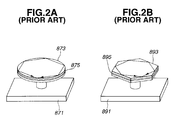
- Devices as illustrated in Figs. 1, 2A and 2B are known, as examples of such a laser.
- the device of Fig. 1 is a surface emitting semiconductor laser in which distributed Bragg reflectors 753 and 755 are provided above and under an active layer 751, respectively, a current can be injected into the active layer 751 through upper and lower electrodes 758 and 759, and its cavity is constructed perpendicular to the substrate 757.
- the devices of Figs. 2A and 2B are disc-type semiconductor lasers in which there are arranged discs 873 and 893 having diameters of about several microns and including circular and hexagonal active layers 875 and 895 above substrates 871 and 891, respectively in which and light is totally reflected at peripheral surfaces of those discs 873 and 893, which thus provide ring cavities in planes parallel to the substrates 871 and 891, respectively.
- the surface emitting semiconductor laser as illustrated in Fig. 1 needs distributed Bragg reflectors with high reflectivity.
- an AlAs/(Al)GaAs multi-layer mirror is ordinarily used as the reflector.
- more than twenty pairs of AlAs/(Al)GaAs are needed to obtain a sufficiently high reflectivity, and hence it takes much time to grow those pairs on a wafer.
- the circular disc is ordinarily formed by dry-etching a predetermined portion after the crystalline growth. Therefore, it is difficult to precisely form the circular periphery of the disc's side, and the side face of the active layer is likely to be damaged. In addition, it is also difficult in this case to further lower the reduced threshold since light propagating in directions parallel or slanting to the substrate is not strongly coupled to the cavity mode.
- oscillation basically occurs in a linearly-polarized light mode
- a semiconductor laser capable of oscillating in a circularly-polarized or elliptically-polarized light mode has not yet been put into practical use.
- An object of the present invention is to provide a ring cavity laser which needs no or only one multi-layer mirror having a high reflectivity, is suitable for a micro-cavity structure, can be readily fabricated, improves a coupling rate of spontaneous radiation light to an oscillation mode, can achieve a low threshold, and is capable of oscillating even with circularly-polarized or elliptically-polarized light.
- the present invention is generally directed to a ring cavity laser which has a polyhedral structure contoured by a plurality of planes, includes a ring cavity having reflective faces formed by the planes of the polyhedral structure, and an active medium, and is constructed such that there exists a three-dimensional light path (i.e., one which is not contained in a single plane) among light paths of the ring cavity through which light pumped in the active medium travels when this light starts at a point on one reflective face, is reflected by each reflective face and returns to the starting point.
- This fundamental structure is capable of increasing a degree of light confinement, enhancing a coupling rate of spontaneous light to its cavity mode, and effecting oscillation even with circularly-polarized or elliptically-polarized light.
- a ring cavity laser which can be readily fabricated by using a selective etching method, a selective growth method and the like (which will be described later), and lower its threshold. Since the laser can oscillate with circularly-polarized or elliptically-polarized light, a light source having a strong resistivity to noise, such as returning light, can be built in optical communication systems, for example, when the laser is used as such a light source.
- the ring cavity can be constructed such that light is totally reflected at at least one reflective point of the plural reflective points in its three-dimensional light path.
- the ring cavity can be constructed such that light is totally reflected at all the reflective points in its three-dimensional light path.
- a cavity with little cavity loss can thus be built. Where light is totally reflected at all the reflective points, a cavity with little cavity loss can be constructed without using any multi-layer mirrors.
- the polyhedral structure can be a tetrahedron or specifically a regular tetrahedron. More specifically, the polyhedral structure can be formed of a semiconductor of zinc-blende-type crystalline structure. Such a structure can be easily fabricated by using known semiconductor processing techniques.
- the semiconductor tetrahedron can include three ⁇ 111 ⁇ B faces, three ⁇ 111 ⁇ A faces, or three ⁇ 110 ⁇ faces.
- Those configurations can be readily fabricated by a selective growth method using a face-orientation dependence, or a selective etching method using a face-orientation dependence. Accordingly, a polyhedron having flat reflective faces can be easily obtained. Further, a minute tetrahedron can be fabricated.
- the polyhedron or tetrahedron can be constructed by performing the selective growth on a substrate having a principal plane of a (111)A face.
- Semiconductor faces of ( 1 11)B, (1 1 1)B and (11 1 )B faces appear during the selective growth.
- the polyhedron or tetrahedron can be constructed by performing the selective growth on a substrate having a principal plane of a (111)A face.
- Semiconductor faces of (011), (101) and (110) faces appear during the selective growth.
- the polyhedron or tetrahedron can be constructed by performing the selective growth on a substrate having a principal plane of a (111)B face.
- Semiconductor faces of ( 11 1)A, ( 1 1 1 )A and (1 11 )A faces appear during the selective growth.
- the polyhedron or tetrahedron can be constructed by performing the selective growth on a substrate having a principal plane of a (111)B face.
- Semiconductor faces of (0 11 ), ( 1 0 1 ) and ( 11 0) faces appear during the selective growth.
- the polyhedral ring cavity can be readily fabricated by those selective growths.
- the polyhedron or tetrahedron can be constructed by selectively etching a substrate having a principal plane of a (111)B face.
- Semiconductor faces of ( 11 1)A, ( 1 1 1 )A and (1 11 )A faces appear during the etching process.
- the polyhedral ring cavity can also be readily fabricated by this selective etching method.
- At least one reflective face of the ring cavity can be formed by a multi-layer reflector. More specifically, this film may be a semiconductor multi-layer reflector or a dielectric multi-layer reflector. A reflective face having a high reflectivity can thus be formed, and hence losses in the cavity can be reduced.
- the polarization state of an oscillation mode can be set by using the fact that a phase shift in reflection at the multi-layer is zero. Further, where the semiconductor multi-layer reflector is used, a reflective face on the substrate can be readily obtained since this semiconductor reflector can be formed during a crystal growth process on the substrate.
- the polyhedral ring cavity can be formed on a semiconductor substrate.
- side faces other than a bottom face of the polyhedron can be covered with a buried material whose index of refraction is smaller than that of semiconductor of the ring cavity such that the total reflection condition can be met.
- the polyhedral ring cavity can be formed on a semiconductor substrate which has a face inclining toward a predetermined direction by a predetermined angle from a (111)A or (111)B face. Since the shape of the polyhedron or tetrahedron can be appropriately set in such a structure, a readily oscillating cavity mode and the polarization state of an oscillating mode can be properly determined.
- the principle of the present invention will be described using a tetrahedron ABCD shown in Figs. 3A-3D.
- the tetrahedron includes a-, b-, c- and d-faces. There is a light path through which light starting at a point L on the a-face is reflected at a point M on the d-face, at a point N on the b-face and at a point P on the c-face, and returns to the point L.
- the tetrahedron ABCD is a regular tetrahedron, the incident angle of the light on each face is 39.23° .
- the tetrahedron ABCD is immersed in air, whose index of refraction is 1 (one), the light will be totally reflected on each face of the tetrahedron, as is known from the well-known Snell's law, provided that the material of the tetrahedron ABCD has an index of refraction (n) more than 1.58 (n>1.58). Since power reflectance upon total reflection is 100%, the reflection is accompanied by no loss. A cavity with little cavity loss can thus be constructed without needing any special multi-layer mirrors.
- a complete establishment of the cavity requires satisfaction of another condition, that the returning light should have the same polarization state as that of the original light.
- the electric field of light is separated into a p-component (its field component is parallel to the incident plane) and an s-component (its field component is normal to the incident plane).
- a phase-shift amount occurring at the time of total reflection will be considered.
- E p and E s are p- and s-components of the electric field of light incident on the point L on the a-face, respectively
- E p ' and E s ' are p- and s-components of the electric field of light returning to the point L after one round
- M is a phase-shift matrix representing phase shifts which light receives on the respective faces during one round of the light path
- L is the length of the cavity
- k 2N ⁇ / ⁇
- N is the index of refraction of the tetrahedron
- ⁇ is the wavelength of the light.
- the phase-shift matrix M is a product of a matrix representing phase shifts received by p- and s-components at the time of reflection on each face and a matrix representing conversions between p- and s-directions in the path from one face to the next face.
- an eigenvalue ⁇ 0 and an eigenvector having a p-component of E p0 and an s-component of E s0 exist without exception, and satisfy: Provided that no loss is present (this assumption does not impair generality and is permissible because, even if there is actually some loss, a gain compensating for this loss can be given), the determinant of the phase-shift matrix M is 1 (one) and the eigenvalue ⁇ 0 thereof is a complex quantity whose absolute value is 1 (one) (i.e., exp( ⁇ pure imaginary number).
- This polarized light is generally elliptically-polarized or circularly-polarized light both components of which have non-zero amplitudes, and have a certain phase difference therebetween.
- the matrix M is a 2 ⁇ 2 matrix, there normally exist two eigenvalues. Those correspond to right-handed and left-handed elliptically polarized light, respectively.
- elliptically-polarized light can be lased in the thus-constructed three-dimensional ring cavity. It is also possible to lase circularly-polarized or linearly-polarized light when the phase-shift amount at the time of reflection is regulated by controlling an index difference and a structure at the interface of the reflective face, or when the shape of the tetrahedron is controlled (e.g., a regular tetrahedron or a predetermined tetrahedron is built), or when another polyhedron is used.
- the light path having reflection points on the a-, d-, b-, c- and a-faces in this order, but the light path may have other routes.
- light may be reflected twice or more on the same face in a cavity.
- Such a cavity mode is generally present in the structure of this invention.
- a readily lasing cavity mode can be specifically determined by appropriately defining the shape of the cavity (e.g., shaping the cavity into a tetrahedron other than a regular tetrahedron).
- fabricating methods of the polyhedron or tetrahedron there are a selective growth method using the face-orientation dependence, and a selective etching method using the face-orientation dependence.
- a sufficiently flat face can be obtained by those methods, as compared with fabrication by dry etching.
- this invention makes it easy to fabricate a polyhedron or tetrahedron with sides of about several microns, a micro-cavity structure can be readily formed.
- the number of bonds is three on a ⁇ 111 ⁇ B face. Therefore, the stability of As atoms on the uppermost face is high, so the growth rate increases as the temperature rises and the V/III supply ratio decreases, conversely to the case of the ⁇ 111 ⁇ A face.
- the tetrahedral structure can be formed by using this difference in the growth rate.
- a mask for the selective growth which has a window of a regular triangle having three sides extending in the ⁇ 0 1 1>, ⁇ 10 1 > and ⁇ 1 10> directions, is formed on a substrate with a (111)B face, and crystal is grown under conditions of a high temperature and a small V/III supply ratio. Then, since little growth of a ⁇ 111 ⁇ A face occurs, a triangular cone can be formed with (1 11 )A, ( 1 1 1 )A and ( 11 1)A as terminal faces.
- the tetrahedral structure can be completed by removing the substrate from its bottom by etching.
- a mask for the selective growth which has a window in the shape of an equilateral triangle having three sides extending in the ⁇ 0 1 1>, ⁇ 10 1 > and ⁇ 1 10> directions, is formed on a substrate with a (111)A face, and crystal is grown under conditions of a low temperature and a large V/III supply ratio. Then, since little growth of a ⁇ 111 ⁇ B face occurs, a triangular cone can be formed with ( 1 11)B, (1 1 1)B and (11 1 )B as terminal faces.
- a tetrahedron can be formed by using a difference in the growth rate between a ⁇ 011 ⁇ face and a ⁇ 111 ⁇ A or ⁇ 111 ⁇ B face.
- the substrate face is a complete ⁇ 111 ⁇ face, a regular tetrahedron can be formed.
- a so-called off substrate in which a face orientation is shifted by a predetermined angle, is used, the shape of the tetrahedron can be controlled.
- etching when etching is performing using an etching liquid, such as Br 2 -C 2 H 5 OH, a tetrahedron can be formed since the etching rate of a ⁇ 111 ⁇ A face is quite low.
- an etching liquid such as Br 2 -C 2 H 5 OH
- Fig. 1 is a cross-sectional view of a prior-art surface emitting semiconductor laser.
- Figs. 2A and 2B are perspective views illustrating prior-art disc-type semiconductor lasers, respectively.
- Figs. 3A-3D are views illustrating a ring cavity laser constructed according to an embodiment of the present invention.
- Fig. 4 is a cross-sectional view of a first embodiment of a ring cavity laser according to the present invention.
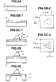
- Figs. 5A to 5E are cross-sectional views for explaining a fabrication process of the first embodiment.
- Figs. 6A to 6E are cross-sectional views for explaining a fabrication process of a third embodiment of a ring cavity laser according to the present invention.
- Fig. 7 is a cross-sectional view of a fourth embodiment of a ring cavity laser according to the present invention.
- Fig. 8 is a cross-sectional view of a fifth embodiment of a ring cavity laser according to the present invention.
- Figs. 9A-9D are views illustrating a ring cavity laser constructed according to the present invention, respectively.
- Fig. 10 is a cross-sectional view of a sixth embodiment of a ring cavity laser according to the present invention.
- Figs. 11A-11D are views illustrating a ring cavity laser constructed according to the present invention, respectively.
- Fig. 12 is a cross-sectional view of a seventh embodiment of a ring cavity laser according to the present invention.
- n-AlAs etching stop layer 13 having a thickness of 0.2 ⁇ m, and an n-Al 0.2 Ga 0.8 As clad layer 15 having a thickness of 1.0 ⁇ m are serially grown on an n-GaAs substrate 11 having a (111)B face, using an MOCVD method (see Fig. 5A).
- a window of an equilateral triangle having three sides extending in ⁇ 0 1 1>, ⁇ 10 1 > and ⁇ 1 10> directions is formed in the SiO 2 by etching to form a mask 17 for the selective growth.
- the length of each side of the equilateral triangle is 5 ⁇ m (see Figs. 5B-1 and 5B-2).
- an n-Al 0.2 Ga 0.8 As clad layer 19 having a thickness of 1.0 ⁇ m, an n-GaAs active layer 21 having a thickness of 0.2 ⁇ m, a p-Al 0.2 Ga 0.8 As clad layer 23 having a thickness of 2.0 ⁇ m, a p-Al 0.3 Ga 0.7 As contact layer 25 having a thickness of 0.3 ⁇ m are serially grown under conditions of a low temperature and a large V/III supply ratio.
- a triangular cone can be formed with (1 11 )A, ( 1 1 1 )A and ( 11 1)A as terminal faces (see Figs. 5C-1 and 5C-2).
- n-side annular electrode 27 is formed on the bottom face of the substrate 11, and a p-side electrode 29 is formed on the top contact layer 25 (see Fig. 5D).
- the substrate 11 is wet-etched from its bottom face with an etching liquid of ammonia plus hydrogen peroxide series, and the etching stop layer 13 is etched with hydrofluoric acid.
- the clad layer 15 is thus exposed to be a reflective face (see Fig. 5E).
- the thus-fabricated ring cavity semiconductor laser has a light path in a three-dimensional ring cavity as illustrated in Figs. 3A-3D.
- the incident angle on each face is 39.23° .
- This value meets the total reflection condition at the interface between the semiconductor (its index of refraction is about 3.2) and air.
- a cavity with low loss can thus be built without using any multi-layer mirrors as used in the surface emitting semiconductor laser.
- evanescent light created near the reflective face at the time of total reflection can also be used by coupling it to an exterior waveguide, such as an optical fiber.
- the substrate having the (111)B face is used in this embodiment, but a (111)A face can likewise be used.
- the selective growth is performed under the condition that the growth rate of the ⁇ 111 ⁇ B face is much smaller than that of the ⁇ 111 ⁇ A face, i.e., under a low temperature and a small V/III supply ratio.
- a tetrahedron having a side of the ⁇ 111 ⁇ B face can be formed.
- the substrate having the (111)B face is used in the first embodiment, but crystal can also be grown using a so-called off substrate.
- crystal is grown on a (111)B substrate whose face is inclined seven degrees toward a ⁇ 2 11 > direction, and a ring cavity semiconductor laser is thus fabricated. Its growth method and so forth are substantially the same as those used in the first embodiment.
- the cavity since the cavity has the regular tetrahedral structure, there are three light paths in the ring cavity which are mutually in a triple symmetrical relation about a normal to the substrate 11. Each of the three light paths has forward and reverse directions. Consequently, when current sufficiently larger than the threshold is injected into the active layer 21, the scattering light generated at the interface between the semiconductor and the electrode 29 has an intensity distribution which has directivities in six directions.
- the scattering light has two directivities (forward and reverse directions in the same light path) in the second embodiment.
- the symmetry of the tetrahedron can be eliminated by inclining the substrate face.
- possible ring cavities can be differentiated with respect to their thresholds, and a most-readily lasing cavity mode can thus be determined.
- tetrahedral cavity is formed by using the selective growth.
- a polyhedron can be formed by a selective etching using the face-orientation dependence likewise.
- a third embodiment is directed to such a structure.
- Figs. 6A-6E illustrate respective steps of a fabrication method of a ring cavity semiconductor laser of this embodiment. The fabrication method will be described.
- the clad layer 119 and the contact layer 121 are etched by using a Br 2 -C 2 H 5 OH etching liquid.
- a triangular cone can be formed with terminal (1 11 )A, ( 1 1 1 )A and ( 11 1)A as terminal faces (see Figs. 6C-1 and 6C-2).
- an n-side annular electrode 125 is formed on the bottom face of the substrate 111, and a p-side electrode 127 is formed on the top contact layer 121 (see Fig. 6D).
- the substrate 111 is wet-etched from its bottom face with an etching liquid of ammonia plus hydrogen peroxide series, and the etching stop layer 113 is etched with hydrofluoric acid.
- the clad layer 115 is thus exposed to be a reflective face (see Fig. 6E).
- the reflective face is formed by etching having face-orientation dependence, reflective faces with smaller loss than that formed by dry etching such as RIE, can be formed.
- the process of the third embodiment is simplified, since only one crystalline growth is needed.
- the third embodiment is the same as the first embodiment.
- FIG. 7 shows a cross-section of a ring cavity semiconductor laser of this embodiment.
- the fourth embodiment differs from the first embodiment in that slant side faces of a semiconductor tetrahedron is covered with insulating material.
- the semiconductor layer structure and so forth of the fourth embodiment are substantially the same as those of the first embodiment.
- Fig. 7 the same functional layers as those of the first embodiment are denoted by the same reference numerals as those in Fig. 4.
- a buried layer 201 is formed of Al 2 O 3 deposited by the sputtering method.
- the index of refraction of Al 2 O 3 is normally about 1.62, so the incident angle of 39.23° satisfies the total reflection condition. Therefore, the light confinement of this embodiment is as good as the first embodiment. The cavity loss is thus little, and hence a ring cavity semiconductor laser with low threshold can be achieved.
- a difference in the index of refraction can be controllably changed between the cavity semiconductor and the buried layer 201 by selecting the material of the buried layer 201.
- the phase at the time of total reflection is accordingly varied, so that a degree of elliptical polarization in oscillation can be controlled.
- a p-side electrode 229 can be deposited over the top portion of the cavity and the buried layer 201. No special patterning process is hence needed to form the electrode 229. Moreover, reflection loss at the semiconductor slant face due to unwanted extension of the electrode thereto can be eliminated.
- the p-side of this embodiment is bonded to a heat sink with solder or the like to form a thermal radiation mechanism
- unwanted extension of the solder to the reflective face can be prevented by the burying layer 201.
- the fabrication can thus be facilitated.
- radiation efficiency can be increased.
- thermal conductivity of Al 2 O 3 is great, so the radiation efficiency can be further improved.
- SiO 2 , SiN x , AlN, MgO or polyimide can also be used in place of Al 2 O 3 , for example. Materials having a large thermal conductivity are naturally preferable to obtain a better effect.
- FIG. 8 shows a cross-section of a ring cavity semiconductor laser of this embodiment.
- the fifth embodiment differs from the first embodiment in that a semiconductor multi-layer mirror 301 of AlAs/GaAs is provided between the substrate 11 and the clad layer 15 while no etching stop layer is provided.
- the semiconductor layer structure and so forth of the fifth embodiment are substantially the same as those of the first embodiment.
- the same functional layers as those of the first embodiment are denoted by the same reference numerals as those in Fig. 4.
- etching of the substrate performed in the first embodiment is not needed, so fabrication is further facilitated.
- reflection by the multi-layer mirror is different from the total reflection at the interface between semiconductor and air and is not accompanied by a phase shift, oscillation in an elliptical polarization mode, which differs from that in the first embodiment, can be obtained.
- the ring-cavity light path formed in the tetrahedron can have various patterns. This fact will be described with reference to Figs. 9A-9D which are respectively perspective, plan, front and side views showing different aspects of a ring cavity. In this case, a plurality of reflections occur on a cirtain face during one round of the ring cavity.
- FIG. 10 shows a cross section of a ring cavity semiconductor laser of the sixth embodiment.
- the semiconductor layer structure and so forth of the sixth embodiment are substantially the same as those of the first embodiment.
- the same functional layers as those of the first embodiment are denoted by the same reference numerals as those in Fig. 4.
- a clad layer 415 is made thinner than that of the first embodiment and the active layer 421 is formed directly on the thin clad layer 415 during the selective growth without interposing a clad layer.
- the thickness of a clad layer 423 can be reduced, so that the growth time can be shortened, as compared with the first embodiment. Further, since the area of a contact layer 425 can be expanded, a p-side electrode 429 can be further facilitated and its contact resistance can be lowered.
- the position of the active layer in the tetrahedron is changed in the above manner, so oscillation can be further efficiently effected in a cavity mode different from that of the first embodiment.
- three side faces of the tetrahedron are ⁇ 111 ⁇ A faces or ⁇ 111 ⁇ B faces. Side faces, however, are not limited to these. For example, ⁇ 011 ⁇ faces are possible.
- Figs. 11A-11D and 12 illustrate such an example. Figs. 11A-11D are respectively perspective, plan, front and side views showing different aspects of a ring cavity.
- Fig. 12 illustrates a cross-section of a ring cavity semiconductor laser of the seventh embodiment.
- a fabrication method of this embodiment will be initially described with reference to Fig. 12.
- the fabrication method is substantially the same as that of the first embodiment.
- n-AlAs etching stop layer 513 having a thickness of 0.2 ⁇ m, and an n-Al 0.2 Ga 0.8 As clad layer 515 having a thickness of 1.0 ⁇ m are serially grown on an n-GaAs substrate 511 having a ⁇ 111 ⁇ B face, using the MOCVD method.
- a window having the shape of an equilateral triangle whose three sides extend in ⁇ 0 1 1>, ⁇ 10 1 > and ⁇ 1 10> directions is formed in the SiO 2 by etching to form a mask 517 for the selective growth.
- an n-Al 0.2 Ga 0.8 As clad layer 519 having a thickness of 0.5 ⁇ m, a GaAs active layer 521 having a thickness of 0.2 ⁇ m, a p-Al 0.2 Ga 0.8 As clad layer 523 having a thickness of 1.0 ⁇ m, and a p-Al 0.3 Ga 0.7 As contact layer 525 having a thickness of 0.3 ⁇ m are serially grown on conditions of a low temperature and a large V/III supply ratio. Under those conditions, the growth rate of a ⁇ 111 ⁇ B face is large.
- the growth condition is so selected that the growth rate of the ⁇ 111 ⁇ A face is larger than that of the ⁇ 011 ⁇ face.
- a triangular cone with three ⁇ 011 ⁇ faces as terminal faces, i.e., (0 11 ), ( 1 0 1 ) and ( 11 0) faces, can be formed.
- an n-side annular electrode 527 is formed on the bottom face of the substrate 511, and a p-side electrode 529 is formed on the top contact layer 525.
- the substrate 511 is wet-etched from its bottom face with an etching liquid of ammonia plus hydrogen peroxide series, and the etching stop layer 513 is etched with hydrofluoric acid.
- the clad layer 515 is thus exposed to be a reflective face.
- the thus-fabricated ring cavity will be described with reference to Figs. 11A-11D.
- Light starting at a point E on an a-face is reflected at a point F on a d-face, and returns to the a-face.
- the light is then reflected at a point H on the a-face, at a point I on a b-face, at a point J on the a-face and at a point K on a c-face, and again returns to the point E.
- the cavity is established.
- the incident angles on each side face and the bottom face are respectively 18.43° and 39.23° , and those values satisfy the total reflection condition when the polyhedral cavity is composed of semiconductor whose index of refraction is about 3.2. A cavity with low loss can thus be built.
- the layer thickness of the selective growth can be smaller than that of the first embodiment.
- oscillation can be effected in a cavity mode different from that of the first embodiment by changing the shape of the tetrahedron.
- a triangular cone with three (011) faces as terminal faces may be formed on a substrate having a ⁇ 111 ⁇ A face by selecting appropriate growth conditions.
- the active layer is pumped by the current injection, but the pumping method is not limited thereto.
- the pumping can also be effected by introducing pumping light into the active layer from outside.
- III - V compound semiconductor such as InGaAsP/InP, GaInP/GaAs and GaInNAs/GaAs, mixed crystal materials formed therefrom, II - VI compound semiconductors, such as ZnSe/GaAs, or mixed crystal materials formed therefrom can be used likewise.
- II - VI compound semiconductors such as ZnSe/GaAs, or mixed crystal materials formed therefrom can be used likewise.
- a p-type substrate can also be used in the above embodiments.
- growth methods such as MBE and CBE
- MOCVD metal-organic chemical vapor deposition
- the semiconductor multi-layer is used in the above embodiment.
- dielectric multi-layers such as SiO 2 /Si, Al 2 O 3 /Si and SiO 2 /TiO 2 , can be used likewise.
- tetrahedral structures are adopted, but other polyhedrons, such as a tetrahedral cone, that can provide three-dimensional ring cavities, can also be adopted.
- the material of the cavity is not limited to semiconductors, and the cavity can be composed of other material, such as organic materials, glass (in this case, a polyhedral glass cavity is disposed on the active medium, for example), and combinations of different materials.
- the active medium is not likewise limited to semiconductor materials.
Landscapes
- Physics & Mathematics (AREA)
- Condensed Matter Physics & Semiconductors (AREA)
- General Physics & Mathematics (AREA)
- Electromagnetism (AREA)
- Optics & Photonics (AREA)
- Semiconductor Lasers (AREA)
- Lasers (AREA)
Applications Claiming Priority (2)
| Application Number | Priority Date | Filing Date | Title |
|---|---|---|---|
| JP21197798 | 1998-07-10 | ||
| JP21197798A JP3658194B2 (ja) | 1998-07-10 | 1998-07-10 | リング共振器型レーザ |
Publications (2)
| Publication Number | Publication Date |
|---|---|
| EP0971463A2 true EP0971463A2 (fr) | 2000-01-12 |
| EP0971463A3 EP0971463A3 (fr) | 2001-01-31 |
Family
ID=16614852
Family Applications (1)
| Application Number | Title | Priority Date | Filing Date |
|---|---|---|---|
| EP99305470A Withdrawn EP0971463A3 (fr) | 1998-07-10 | 1999-07-09 | Laser à cavité annulaire |
Country Status (3)
| Country | Link |
|---|---|
| US (1) | US6282226B1 (fr) |
| EP (1) | EP0971463A3 (fr) |
| JP (1) | JP3658194B2 (fr) |
Cited By (11)
| Publication number | Priority date | Publication date | Assignee | Title |
|---|---|---|---|---|
| EP1758218A3 (fr) * | 2005-08-22 | 2008-12-31 | Avago Technologies ECBU IP (Singapore) Pte. Ltd. | Système à semiconducteur comprenant un laser à cavité à anneau fabriqué par croissance de recouvrement épitaxiale |
| US8947221B2 (en) | 2013-02-26 | 2015-02-03 | Ford Global Technologies, Llc | Method and apparatus for tracking device connection and state change |
| US9064101B2 (en) | 2011-04-01 | 2015-06-23 | Ford Global Technologies, Llc | Methods and systems for authenticating one or more users of a vehicle communications and information system |
| US9079554B2 (en) | 2011-08-09 | 2015-07-14 | Ford Global Technologies, Llc | Method and apparatus for vehicle hardware theft prevention |
| CN103972789B (zh) * | 2014-04-04 | 2017-01-11 | 南京邮电大学 | 氮化物非对称型回音壁模式光学微腔器件及制备方法 |
| US9612999B2 (en) | 2013-03-13 | 2017-04-04 | Ford Global Technologies, Llc | Method and system for supervising information communication based on occupant and vehicle environment |
| US9639688B2 (en) | 2010-05-27 | 2017-05-02 | Ford Global Technologies, Llc | Methods and systems for implementing and enforcing security and resource policies for a vehicle |
| US9688246B2 (en) | 2013-02-25 | 2017-06-27 | Ford Global Technologies, Llc | Method and apparatus for in-vehicle alarm activation and response handling |
| US10249123B2 (en) | 2015-04-09 | 2019-04-02 | Ford Global Technologies, Llc | Systems and methods for mobile phone key fob management |
| US10486716B2 (en) | 2011-02-10 | 2019-11-26 | Ford Global Technologies, Llc | System and method for controlling a restricted mode in a vehicle |
| CN111952839A (zh) * | 2020-08-21 | 2020-11-17 | 中国科学院半导体研究所 | 半导体激光器 |
Families Citing this family (14)
| Publication number | Priority date | Publication date | Assignee | Title |
|---|---|---|---|---|
| JP2001165666A (ja) * | 1999-12-07 | 2001-06-22 | Canon Inc | 角速度検出装置 |
| JP3619155B2 (ja) | 2001-01-17 | 2005-02-09 | キヤノン株式会社 | 面発光レーザ装置、その製造方法、およびその駆動方法 |
| CN100405519C (zh) * | 2003-03-27 | 2008-07-23 | 清华大学 | 一种场发射元件的制备方法 |
| KR100611055B1 (ko) * | 2004-03-25 | 2006-08-10 | 학교법인 포항공과대학교 | 광양자테 레이저의 다파장 발진특성을 이용한 저전력디스플레이 소자 |
| CN1959896B (zh) | 2005-11-04 | 2011-03-30 | 鸿富锦精密工业(深圳)有限公司 | 碳纳米管场发射体及其制备方法 |
| US7557972B2 (en) * | 2006-06-07 | 2009-07-07 | Canon Kabushiki Kaisha | Oscillator device, optical deflector and optical instrument using the same |
| US7813390B2 (en) | 2007-08-29 | 2010-10-12 | Pavilion Integration Corporation | Injection-seeded monolithic laser |
| CN102017336B (zh) * | 2008-05-06 | 2012-07-04 | 惠普开发有限公司 | 微环形激光器系统和方法 |
| WO2011078147A1 (fr) * | 2009-12-21 | 2011-06-30 | 国立大学法人大阪大学 | Materiau reflechissant et structure optique |
| US8788113B2 (en) | 2011-06-13 | 2014-07-22 | Ford Global Technologies, Llc | Vehicle driver advisory system and method |
| US9002536B2 (en) | 2013-03-14 | 2015-04-07 | Ford Global Technologies, Llc | Key fob security copy to a mobile phone |
| US9786602B2 (en) | 2015-08-21 | 2017-10-10 | Taiwan Semiconductor Manufacturing Company, Ltd. | Interconnection structure and methods of fabrication the same |
| CN109698464B (zh) * | 2018-12-26 | 2020-07-28 | 中南大学 | 一种垂直结构电注入金字塔微腔激光器及其制备方法 |
| RU2713561C1 (ru) * | 2019-05-28 | 2020-02-05 | Федеральное государственное бюджетное научное учреждение "Федеральный исследовательский центр Институт прикладной физики Российской академии наук" (ИПФ РАН) | Дисковый лазерный неустойчивый резонатор для обеспечения выходного лазерного сигнала с близким к дифракционному качеством пучка |
Family Cites Families (10)
| Publication number | Priority date | Publication date | Assignee | Title |
|---|---|---|---|---|
| US4818087A (en) * | 1982-08-27 | 1989-04-04 | Raytheon Company | Orthohedral ring laser gyro |
| US4578793A (en) * | 1984-07-13 | 1986-03-25 | The Board Of Trustees Of The Leland Stanford Junior University | Solid-state non-planar internally reflecting ring laser |
| US5080487A (en) | 1986-11-06 | 1992-01-14 | Litton Systems, Inc. | Ring laser gyroscope with geometrically induced bias |
| US4747111A (en) | 1987-02-13 | 1988-05-24 | Hewlett-Packard Company | Quasi-planar monolithic unidirectional ring laser |
| JPH04216691A (ja) | 1990-12-17 | 1992-08-06 | Sony Corp | 半導体レーザ装置とその製法 |
| US6009115A (en) * | 1995-05-25 | 1999-12-28 | Northwestern University | Semiconductor micro-resonator device |
| US5825799A (en) * | 1995-05-25 | 1998-10-20 | Northwestern University | Microcavity semiconductor laser |
| US5878070A (en) * | 1995-05-25 | 1999-03-02 | Northwestern University | Photonic wire microcavity light emitting devices |
| DE19702681C2 (de) * | 1997-01-25 | 1999-01-14 | Lzh Laserzentrum Hannover Ev | Nichtplanarer Ringlaser mit Güteschaltung im Einfrequenzbetrieb |
| US6134257A (en) * | 1998-04-21 | 2000-10-17 | Lucent Technologies Inc. | Solid state laser for operation in librational modes |
-
1998
- 1998-07-10 JP JP21197798A patent/JP3658194B2/ja not_active Expired - Fee Related
-
1999
- 1999-07-09 EP EP99305470A patent/EP0971463A3/fr not_active Withdrawn
- 1999-07-09 US US09/349,472 patent/US6282226B1/en not_active Expired - Fee Related
Cited By (13)
| Publication number | Priority date | Publication date | Assignee | Title |
|---|---|---|---|---|
| EP1758218A3 (fr) * | 2005-08-22 | 2008-12-31 | Avago Technologies ECBU IP (Singapore) Pte. Ltd. | Système à semiconducteur comprenant un laser à cavité à anneau fabriqué par croissance de recouvrement épitaxiale |
| US9639688B2 (en) | 2010-05-27 | 2017-05-02 | Ford Global Technologies, Llc | Methods and systems for implementing and enforcing security and resource policies for a vehicle |
| US10486716B2 (en) | 2011-02-10 | 2019-11-26 | Ford Global Technologies, Llc | System and method for controlling a restricted mode in a vehicle |
| US9064101B2 (en) | 2011-04-01 | 2015-06-23 | Ford Global Technologies, Llc | Methods and systems for authenticating one or more users of a vehicle communications and information system |
| US10692313B2 (en) | 2011-04-01 | 2020-06-23 | Ford Global Technologies, Llc | Methods and systems for authenticating one or more users of a vehicle communications and information system |
| US9079554B2 (en) | 2011-08-09 | 2015-07-14 | Ford Global Technologies, Llc | Method and apparatus for vehicle hardware theft prevention |
| US9688246B2 (en) | 2013-02-25 | 2017-06-27 | Ford Global Technologies, Llc | Method and apparatus for in-vehicle alarm activation and response handling |
| US8947221B2 (en) | 2013-02-26 | 2015-02-03 | Ford Global Technologies, Llc | Method and apparatus for tracking device connection and state change |
| US9612999B2 (en) | 2013-03-13 | 2017-04-04 | Ford Global Technologies, Llc | Method and system for supervising information communication based on occupant and vehicle environment |
| CN103972789B (zh) * | 2014-04-04 | 2017-01-11 | 南京邮电大学 | 氮化物非对称型回音壁模式光学微腔器件及制备方法 |
| US10249123B2 (en) | 2015-04-09 | 2019-04-02 | Ford Global Technologies, Llc | Systems and methods for mobile phone key fob management |
| CN111952839A (zh) * | 2020-08-21 | 2020-11-17 | 中国科学院半导体研究所 | 半导体激光器 |
| CN111952839B (zh) * | 2020-08-21 | 2022-07-19 | 中国科学院半导体研究所 | 半导体激光器 |
Also Published As
| Publication number | Publication date |
|---|---|
| EP0971463A3 (fr) | 2001-01-31 |
| JP2000031586A (ja) | 2000-01-28 |
| JP3658194B2 (ja) | 2005-06-08 |
| US6282226B1 (en) | 2001-08-28 |
Similar Documents
| Publication | Publication Date | Title |
|---|---|---|
| US6282226B1 (en) | Ring cavity laser | |
| EP0896405B1 (fr) | Procédé de fabrication d'un dispositif semi-conducteur à émission de surface | |
| US7013072B2 (en) | Optical device and optical module | |
| JP2534444B2 (ja) | 集積化短キャビティ・レ―ザ | |
| EP0892474B1 (fr) | Laser à émission de surface à cavité verticale à modulation de champ, avec pompage optique interne | |
| EP1326290A2 (fr) | Méthode de fabrication de structures semiconductrices | |
| US6277696B1 (en) | Surface emitting laser using two wafer bonded mirrors | |
| EP1026798B1 (fr) | Laser à cavité verticale à émission de surface (VCSEL) utilisant des miroirs Bragg enterrées et méthode de fabrication | |
| JP2003513477A (ja) | 一体化された光学的にポンピングされる垂直キャビティ表面発光レーザ用の方法および装置 | |
| JPH10303515A (ja) | 長波長vcsel | |
| CN103636084A (zh) | 激光器 | |
| CN100533880C (zh) | 多级集成光子器件 | |
| JP4054480B2 (ja) | Si基板上の光電融合デバイス構造、その製造方法、及び成膜方法 | |
| US7154927B2 (en) | Surface emitting semiconductor laser and communication system using the same | |
| JP3559680B2 (ja) | リング共振器型面発光半導体レーザ及びその製造法 | |
| JPH05315695A (ja) | 半導体レーザ | |
| JPH07335967A (ja) | 面発光型光半導体素子及びその製造方法 | |
| WO2001080385A1 (fr) | Laser a cavite de resonance adoptant la forme d'un triangle equilateral dont la sortie a une orientation definie | |
| JPH10233558A (ja) | ダイヤモンド層を含む多層膜構造、それを有する光デバイス、およびその作製方法 | |
| JP2002252418A (ja) | 光通信システム | |
| JP2613975B2 (ja) | 周期利得型半導体レーザ素子 | |
| CN112821197A (zh) | 一种光发射芯片的制作方法和光发射芯片 | |
| JP3469051B2 (ja) | 面発光半導体レーザ | |
| JP2005191260A (ja) | 半導体レーザおよびその製造方法および光送信用モジュールおよび光通信システム | |
| JP2000183443A (ja) | スポットサイズ変換器付き半導体レーザ装置、及びその製造方法 |
Legal Events
| Date | Code | Title | Description |
|---|---|---|---|
| PUAI | Public reference made under article 153(3) epc to a published international application that has entered the european phase |
Free format text: ORIGINAL CODE: 0009012 |
|
| AK | Designated contracting states |
Kind code of ref document: A2 Designated state(s): AT BE CH CY DE DK ES FI FR GB GR IE IT LI LU MC NL PT SE |
|
| AX | Request for extension of the european patent |
Free format text: AL;LT;LV;MK;RO;SI |
|
| PUAL | Search report despatched |
Free format text: ORIGINAL CODE: 0009013 |
|
| AK | Designated contracting states |
Kind code of ref document: A3 Designated state(s): AT BE CH CY DE DK ES FI FR GB GR IE IT LI LU MC NL PT SE |
|
| AX | Request for extension of the european patent |
Free format text: AL;LT;LV;MK;RO;SI |
|
| 17P | Request for examination filed |
Effective date: 20010615 |
|
| AKX | Designation fees paid |
Free format text: DE FR GB IT NL SE |
|
| 17Q | First examination report despatched |
Effective date: 20040213 |
|
| GRAP | Despatch of communication of intention to grant a patent |
Free format text: ORIGINAL CODE: EPIDOSNIGR1 |
|
| STAA | Information on the status of an ep patent application or granted ep patent |
Free format text: STATUS: THE APPLICATION IS DEEMED TO BE WITHDRAWN |
|
| 18D | Application deemed to be withdrawn |
Effective date: 20050622 |