EP0971493A2 - Nichtlinearitäts- und Farbenzerstreuungskompensierung in faseroptischer Übertragung - Google Patents
Nichtlinearitäts- und Farbenzerstreuungskompensierung in faseroptischer Übertragung Download PDFInfo
- Publication number
- EP0971493A2 EP0971493A2 EP99113578A EP99113578A EP0971493A2 EP 0971493 A2 EP0971493 A2 EP 0971493A2 EP 99113578 A EP99113578 A EP 99113578A EP 99113578 A EP99113578 A EP 99113578A EP 0971493 A2 EP0971493 A2 EP 0971493A2
- Authority
- EP
- European Patent Office
- Prior art keywords
- optical
- signal
- transmission line
- fiber transmission
- optical fiber
- Prior art date
- Legal status (The legal status is an assumption and is not a legal conclusion. Google has not performed a legal analysis and makes no representation as to the accuracy of the status listed.)
- Withdrawn
Links
Images


Classifications
-
- H—ELECTRICITY
- H04—ELECTRIC COMMUNICATION TECHNIQUE
- H04B—TRANSMISSION
- H04B10/00—Transmission systems employing electromagnetic waves other than radio-waves, e.g. infrared, visible or ultraviolet light, or employing corpuscular radiation, e.g. quantum communication
- H04B10/11—Arrangements specific to free-space transmission, i.e. transmission through air or vacuum
-
- H—ELECTRICITY
- H04—ELECTRIC COMMUNICATION TECHNIQUE
- H04B—TRANSMISSION
- H04B10/00—Transmission systems employing electromagnetic waves other than radio-waves, e.g. infrared, visible or ultraviolet light, or employing corpuscular radiation, e.g. quantum communication
- H04B10/25—Arrangements specific to fibre transmission
- H04B10/2507—Arrangements specific to fibre transmission for the reduction or elimination of distortion or dispersion
- H04B10/2513—Arrangements specific to fibre transmission for the reduction or elimination of distortion or dispersion due to chromatic dispersion
- H04B10/2525—Arrangements specific to fibre transmission for the reduction or elimination of distortion or dispersion due to chromatic dispersion using dispersion-compensating fibres
-
- H—ELECTRICITY
- H04—ELECTRIC COMMUNICATION TECHNIQUE
- H04B—TRANSMISSION
- H04B2210/00—Indexing scheme relating to optical transmission systems
- H04B2210/25—Distortion or dispersion compensation
- H04B2210/252—Distortion or dispersion compensation after the transmission line, i.e. post-compensation
-
- H—ELECTRICITY
- H04—ELECTRIC COMMUNICATION TECHNIQUE
- H04B—TRANSMISSION
- H04B2210/00—Indexing scheme relating to optical transmission systems
- H04B2210/25—Distortion or dispersion compensation
- H04B2210/254—Distortion or dispersion compensation before the transmission line, i.e. pre-compensation
Definitions
- the present invention relates generally to compensation for chromatic dispersion and nonlinearity in optical fiber communication, and more particularly to a method for optical fiber communication which can compensate for chromatic dispersion and nonlinearity to allow long-haul transmission, and a terminal device and system for use in carrying out the method.
- optical fiber communication systems each using such an optical fiber as a transmission line have been put to practical use.
- the optical fiber itself has a very wide band.
- a transmission capacity by the optical fiber is actually limited by a system design.
- the most important limitation is due to waveform distortion by chromatic dispersion occurring in the optical fiber.
- the optical fiber attenuates an optical signal at a rate of about 0.2 dB/km, for example. Loss of the optical signal due to this attenuation has been compensated for by adopting an optical amplifier such as an erbium doped fiber amplifier (EDFA) that is a typical example.
- the EDFA has a gain band in a 1.55 ⁇ m band where a silica optical fiber gives a lowest loss.
- the chromatic dispersion that is often referred to simply as dispersion is a phenomenon such that the group velocity of an optical signal in an optical fiber changes as a function of the wavelength (or frequency) of the optical signal.
- an optical signal having a longer wavelength propagates faster than an optical signal having a shorter wavelength in a wavelength region shorter than 1.3 ⁇ m, and the resultant dispersion is usually referred to as normal dispersion.
- the dispersion (whose unit is ps/nm/km) takes on a negative value.
- an optical signal having a shorter wavelength propagates faster than an optical signal having a longer wavelength in a wavelength region longer than 1.3 ⁇ m, and the resultant dispersion is usually referred to as anomalous dispersion.
- the dispersion takes on a positive value.
- optical Kerr effect is a phenomenon such that the refractive index of an optical fiber changes with the power or intensity of an optical signal.
- a change in the refractive index modulates the phase of an optical signal propagating in an optical fiber, resulting in the occurrence of frequency chirping which changes a signal spectrum.
- This phenomenon is known as self-phase modulation (SPM).
- SPM self-phase modulation
- the chromatic dispersion and the optical Kerr effect impart waveform distortion to an optical signal with an increase in transmission distance. Accordingly, to allow long-haul transmission by an optical fiber while ensuring a transmission quality, the chromatic dispersion and the nonlinearity must be controlled, compensated, or suppressed.
- a method for optical fiber communication First, a device for outputting an optical signal having a variable optical power to an optical fiber transmission line is provided. Secondly, the optical signal transmitted by the optical fiber transmission line is converted into an electrical signal. Thirdly, a parameter (e.g., a bit error rate or an eye opening) related to waveform degradation of the electrical signal is detected. Finally, the optical power of the optical signal to be output to the optical fiber transmission line is controlled according to the parameter detected so that the waveform degradation of the electrical signal is improved.
- a parameter e.g., a bit error rate or an eye opening
- nonlinearity of an optical fiber or a nonlinear phenomenon occurring in an optical fiber used as the optical fiber transmission line is dependent on the optical power of an optical signal to be output to the optical fiber.
- the optical power of the optical signal is changed according to the state of the optical fiber transmission line, e.g., according to the kind of an optical fiber used as the optical fiber transmission line, thereby controlling the nonlinearity of the optical fiber. Therefore, long-haul transmission is allowed with a transmission quality being ensured by compensation for chromatic dispersion and nonlinearity.
- a system comprising first and second terminal devices and an optical fiber transmission line connecting the first and second terminal devices.
- the first terminal device comprises an optical transmitter for outputting an optical signal having a variable optical power to the optical fiber transmission line.
- the second terminal device comprises an optical receiver for converting the optical signal transmitted by the optical fiber transmission line into an electrical signal, a monitor unit for detecting a parameter related to waveform degradation of the electrical signal, and means for transmitting supervisory information on the parameter detected to the first terminal, device.
- the first terminal device further comprises a control unit for controlling the optical power according to the supervisory information so that the waveform degradation of the electrical signal is improved.
- a terminal device comprising an optical transmitter for outputting an optical signal having a variable optical power to an optical fiber transmission line; means for receiving supervisory information on a parameter detected in relation to waveform degradation of the optical signal transmitted by the optical fiber transmission line; and means for controlling the optical power according to the supervisory information so that the waveform degradation of the optical signal is improved.
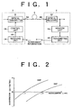
- FIG. 1 is a block diagram showing a basic configuration of the system according to the present invention.
- This system includes a first terminal device 2, a second terminal device 4, and an optical fiber transmission line 6 connecting the first and second terminal devices 2 and 4.
- the first terminal device 2 includes an optical transmitter 8 for outputting an optical signal having a variable optical power to the optical fiber transmission line 6 from its first end 6A, and a control unit 10 for controlling the power of the optical signal to be output from the optical transmitter 8 according to a control signal CS supplied.
- the second terminal device 4 includes an optical receiver 12 for converting the optical signal transmitted by the optical fiber transmission line 6 into an electrical signal, and a monitor unit 14 for detecting a parameter related to waveform degradation of the electrical signal output from the optical receiver 12.
- the second terminal device 4 further includes a transmitting unit 16 for transmitting supervisory information on the parameter detected to the first terminal device 2.
- the first terminal device 2 further includes a receiving unit 18 for receiving the supervisory information transmitted from the second terminal device 4.
- the receiving unit 18 generates the control signal CS to be supplied to the control unit 10 according to the supervisory information so that the waveform degradation of the electrical signal output from the optical receiver 12 is improved.
- the receiving unit 18 generates the control signal CS so that a bit error of the electrical signal output from the optical receiver 12 is reduced or so that an eye opening of the electrical signal output from the optical receiver 12 becomes large.
- the transmission of the supervisory information from the transmitting unit 16 to the receiving unit 18 may be performed by using the optical fiber transmission line 6, by using another optical fiber transmission line (not shown in FIG. 1), or by means of an electrical circuit or a wireless circuit.
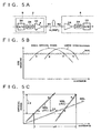
- FIG. 2 is a graph showing dispersion characteristics of optical fibers usable as the optical fiber transmission line 6.
- the vertical axis represents dispersion (ps/nm/km) and the horizontal axis represents wavelength ( ⁇ m).
- the zero-dispersion wavelength of the SMF is about 1.3 ⁇ m.
- the dispersion falls in a region of anomalous dispersion for an optical signal having a wavelength longer than the zero-dispersion wavelength, and has a positive value.
- the dispersion falls in a region of normal dispersion for an optical signal having a wavelength shorter than the zero-dispersion wavelength, and has a negative value.
- the wavelength of an optical signal is set to fall in a 1.55 ⁇ m band (e.g., 1.50 to 1.60 ⁇ m) giving a minimum loss in the SMF. Accordingly, the dispersion for the optical signal falls always in a region of anomalous dispersion.
- the zero-dispersion wavelength of the DSF is about 1.55 ⁇ m.
- the dispersion falls in a region of anomalous dispersion for an optical signal having a wavelength longer than the zero-dispersion wavelength, and has a positive value.
- the dispersion falls in a region of normal dispersion for an optical signal having a wavelength shorter than the zero-dispersion wavelength, and has a negative value.
- the wavelength giving a minimum loss in the DSF is also equal to about 1.55 ⁇ m
- the wavelength of an optical signal is set to fall in a 1.55 ⁇ m band. Accordingly, whether the dispersion in the DSF falls in a region of anomalous dispersion or in a region of normal dispersion is determined according to the correlation between the actual wavelength of an optical signal and the zero-dispersion wavelength of the DSF.
- the optical transmitter 8 in the first terminal device 2 includes an E/O converter (electro/optical converter) 20 for converting an input electrical signal into an optical signal, and a variable gain type optical amplifier 22 for amplifying the optical signal output from the E/O converter 20.
- the gain of the optical amplifier 22 is adjusted by the control unit 10 (see FIG. 1) to thereby change the optical power of the optical signal to be output to the optical fiber transmission line 6.
- an optical amplifier 24 is additionally provided as a preamplifier in the second terminal device 4 in order to enhance a receiver sensitivity.
- the optical amplifier 24 is optically connected between the second end 6B of the optical fiber transmission line 6 and the optical receiver (or an O/E converter (opto/electrical converter) 12.
- FIGS. 4A and 4B there are shown transmission characteristics of a DSF in the anomalous dispersion region and the normal dispersion region, respectively. Attention should be herein directed to the facts that a red-shift chirping is given to an optical signal in the anomalous dispersion region, that a blue-shift chirping is given to an optical signal in the normal dispersion region, and that the chirping given to an optical signal having a large optical power by SPM is always a blue-shift chirping. It is easier to obtain an optical signal having a red-shift chirping than to obtain an optical signal having a blue-shift chirping. Accordingly, it is assumed herein that the optical signal to be output from the optical transmitter 8 has a red-shift chirping.
- the vertical axis represents the eye opening of an equalized signal waveform in the optical receiver 12, and the horizontal axis represents the transmission distance.
- the nonlinearity of the optical fiber transmission line 6 is negligible. Therefore, in the anomalous dispersion region, the red-shift chirping given in the optical transmitter 8 and the red-shift chirping given in the optical fiber transmission line 6 are combined together, and the transmittable distance given by a distance at which the eye opening becomes lower than a waveform degradation limit WDL is relatively short as shown by reference symbol (a) in FIG. 4A.
- the red-shift chirping given in the optical transmitter 8 and the blue-shift chirping given in the optical fiber transmission line 6 are canceled by each other to produce an effect of compression of the waveform or pulse width of the optical signal, so that the transmittable distance is relatively long as shown by reference symbol (d) in FIG. 4B.
- the nonlinearity of the optical fiber transmission line 6 must be considered.
- the blue-shift chirping due to SPM will be dominant at a portion of the optical fiber transmission line 6 in the vicinity of the first end 6A (e.g., a portion at a distance of tens of km).
- the red-shift chirping given in each of the optical transmitter 8 and the optical fiber transmission line 6 and the blue-shift chirping due to SPM are canceled by each other in the anomalous dispersion region, so that the transmittable distance is relatively long as shown by reference symbol (b) in FIG. 4A.
- the blue-shift chirping due to chromatic dispersion and the blue-shift chirping due to SPM are combined together, so that the transmittable distance is relatively short as shown by reference symbol (c) in FIG. 4B.
- FIGS. 3B and 3C show the relation between optical power and distance as converted from FIGS. 4A and 4B, respectively. It is necessary to consider an SN limit of a received signal as a transmission limiting factor.
- the SN limit is denoted by reference symbol SNL.
- reference symbol WDL' in each of FIGS. 3B and 3C corresponds to the waveform degradation limit WDL shown in each of FIGS. 4A and 4B.
- the transmittable distance L1 is determined by the WDL' in the anomalous dispersion region as shown in FIG. 3B, whereas the transmittable distance L2 is determined by the WDL' and the SNL in the normal dispersion region as shown in FIG. 3C. That is, in the system shown in FIG.
- the gain of the optical amplifier 22 is adjusted to thereby adjust the optical power of the optical signal to be output from the optical transmitter 8, so that an optimum condition of compensation for chromatic dispersion and nonlinearity can be obtained to thereby allow long-haul transmission.
- the range of the optical output power from an optical transmitter is fixedly assigned in general to design a system in consideration of variations in the optical power within this range. Accordingly, the transmittable distance L3 is determined (or limited) by the worst condition. To the contrary, by controlling or adjusting the optical power of the optical signal to be output from the optical transmitter 8 by the method according to the present invention, a good transmission quality can always be obtained according to the state of the optical fiber transmission line 6, thereby obtaining a long transmittable distance.
- the system shown in FIG. 5A is characterized in that an SMF is used as the optical fiber transmission line 6.
- an SMF is used as the optical fiber transmission line 6
- the zero-dispersion wavelength of the SMF is about 1.3 ⁇ m
- the wavelength of the optical signal to be output from the optical transmitter 8 falls in a 1.55 ⁇ m band as mentioned previously, so that only an anomalous dispersion region is given.
- dispersion compensating fibers (DCF) 26 and 28 are adopted in this system to compensate for chromatic dispersion in the optical fiber transmission line 6.
- the DCF 26 is optically connected between the E/O converter 20 and the optical amplifier 22, and the DCF 28 is optically connected between the optical amplifier 24 and the O/E converter 12.
- the dispersion compensation for the optical fiber transmission line 6 may be carried out by any one of the DCFs 26 and 28.
- An optical fiber having a dispersion whose absolute value is sufficiently larger than the absolute value of a dispersion in an SMF may be used as each of the DCFs 26 and 28, so as to suppress losses.
- the dispersion in each DCF falls in a normal dispersion region, thereby performing dispersion compensation.
- FIGS. 5B and 5C correspond to FIGS. 4A and 3B, respectively.
- the dispersion induced by these fibers is constant. Accordingly, in each of the cases that the optical power of the optical signal to be output from the optical transmitter 8 is large and small, there exists an optimum value of the distance giving a maximum value of the eye opening as shown in FIG. 5B. Accordingly, in the case that the optical power is small, the transmittable distance is limited to the range between a distance (e) below which the eye opening is lower than the WDL and a distance (f) above which the eye opening is lower than the WDL.
- the transmittable distance is limited to the range between a distance (g) (e ⁇ g) below which the eye opening is lower than the WDL and a distance (h) (f ⁇ h) above which the eye opening is lower than the WDL.
- the condition for obtaining a fixed transmission quality in the system shown in FIG. 5A is given by a region between two lines WDL(#1) and WDL(#2) corresponding to the WDL and on the left side of an SNL as shown in FIG. 5C.
- the transmittable distance falls within a relatively wide range shown by reference symbol L4 in FIG. 5C.
- the range of the optical output power from an optical transmitter is fixedly assigned in general to design a system in consideration of variations in the optical power within this range. Accordingly, the transmittable distance range L5 is determined (or limited) by the worst condition. To the contrary, by controlling or adjusting the optical power of the optical signal to be output from the optical transmitter 8 by the method according to the present invention, a good transmission quality can always be obtained according to the state of the optical fiber transmission line 6, thereby obtaining a long transmittable distance or obtaining a wide transmittable distance range.
- FIG. 6 is a block diagram showing a preferred embodiment of an optical amplifier applicable to the present invention.
- This optical amplifier may be used as the optical amplifier 22 (postamplifier), the optical amplifier 24 (preamplifier), or an optical amplifier included in an optical repeater to be hereinafter described.
- the optical amplifier shown in FIG. 6 includes an input port 30 to which an optical signal to be amplified is supplied, an output port 32 for outputting an optical signal amplified, and an amplifying unit 34 and an optical coupler 36 both provided along a main optical path extending between the input port 30 and the output port 32.
- the amplifying unit 34 includes an optical amplifying medium to which the optical signal from the input port 30 is supplied, and a pumping unit for pumping the optical amplifying medium so that the optical amplifying medium gives a gain to the optical signal supplied.
- the pumping unit is provided by a current source for supplying an injection current to the semiconductor chip. In this case, a gain determined according to the injection current is given to the optical signal.
- an erbium doped fiber (EDF) 38 is used as the optical amplifying medium, so as to adapt it to an optical signal having a wavelength falling in a 1.55 ⁇ m band.
- the EDF 38 has a first end optically connected to the input port 30 and a second end optically connected to the optical coupler 36.
- the pumping unit is provided by a laser diode 40 as a pumping source for supplying pump light having a predetermined wavelength to the EDF 38.
- the wavelength of the pump light is set to fall in a 0.98 ⁇ m band or a 1.48 ⁇ m band, for example.
- bidirectional pumping may be performed by optically connecting a first pumping source through a first WDM coupler to the first end of the EDF 38, and optically connecting a second pumping source through a second WDM coupler to the second end of the EDF 38.
- the laser diode 40 is supplied with a drive current (DC bias current) from a drive circuit 42, so that a gain determined according to the drive current is generated in the EDF 38.
- a drive current DC bias current
- Most of the optical signal amplified in the amplifying unit 34 according to the given gain is passed through the optical coupler 36 and output from the output port 32.
- the remainder of the amplified optical signal is branched off as monitor light by the optical coupler 36, and the monitor light is supplied to a photodetector (PD) 44 such as a photodiode.
- PD photodetector
- the photodetector 44 outputs a signal having a voltage level corresponding to the power of the monitor light received.
- the optical coupler 36 has a branching ratio not dependent on the power of an optical signal supplied, so that the optical power of the optical signal to be output from the output port 32 is reflected by the voltage level of the output signal from the photodetector 44.
- the output signal from the photodetector 44 is supplied to a comparator 46.
- the comparator 46 feedback controls the drive current to be supplied from the drive circuit 42 to the laser diode 40 so that the difference between the voltage level of the output signal from the photodetector 44 and a reference voltage Vref becomes zero or constant.
- the optical power of the optical signal to be output from the output port 32 can be maintained at a constant level determined by the reference voltage Vref (Automatic Level Control: ALC).
- the control unit 10 (see FIG. 1) is provided by a reference voltage generating circuit 48.
- the circuit 48 generates the reference voltage Vref according to the control signal CS supplied. Accordingly, a target value of ALC by this optical amplifier can be predetermined according to the control signal CS.
- FIG. 7 is a block diagram showing a preferred embodiment of the monitor unit 14 shown in FIG. 1.
- An optical signal transmitted by the optical fiber transmission line 6 is amplified by the optical amplifier 24 as a preamplifier, and an amplified optical signal is branched into a first signal beam and a second signal beam by an optical coupler 50.
- the first signal beam is supplied to a first O/E converter (optical receiver) 12.
- the O/E converter 12 regenerates a main signal according to the signal beam received.
- the second signal beam is supplied to a second O/E converter 52 included in the monitor unit 14.
- An output signal from the O/E converter 52 is supplied to an error detecting circuit 54, thereby obtaining error information on a bit error rate of the main signal.
- the O/E converter 52 is supplied with a variable discrimination level, and an eye opening calculating circuit 56 can calculate an eye opening according to the discrimination level and the error information obtained by the error detecting circuit 54. The eye opening thus obtained is provided as eye opening information.
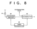
- FIG. 8 there is shown a specific configuration of the O/E converter 52 in the monitor unit 14 shown in FIG. 7.
- the second signal beam from the optical coupler 50 (see FIG. 7) is supplied to a reverse-biased photodiode 57.
- the potential at the anode of the photodiode 57 changes with a change in intensity or optical power due to modulation of the signal beam supplied to the photodiode 57, so that the change in the anode potential is an output electrical signal from the photodiode 57.
- the output electrical signal is equalization-amplified by an equalizing amplifier 58, and an equalization-amplified signal is supplied to a discriminator 62.
- a timing regenerator 60 regenerates a clock according to a signal from the equalizing amplifier 58.
- the discriminator 62 discriminates between a high level and a low level of the equalization-amplified signal at a corresponding timing according to the clock from the timing regenerator 60 and the discrimination level being supplied.
- the O/E converter 12 for the main signal may be obtained by modifying the configuration of the O/E converter 52 shown in FIG. 8 in such a manner that the discrimination level to be supplied to the discriminator 62 becomes constant.
- the parameter (bit error rate or eye opening) related to waveform degradation can be detected by the monitor unit 14 while obtaining the main signal from the O/E converter 12. Accordingly, control of the optical power to an optimum value can be continuously performed even in an in-service condition of the system after initialization thereof.
- the optical coupler 50 and the O/E converter 52 may be omitted, in which an output signal from an equalizing amplifier included in the O/E converter 12 is branched into first and second signals, the first signal being used for demodulation of the main signal, the second signal being used for error detection and eye opening calculation.
- the receiving power of the O/E converter 12 can be increased and the number of optical components can be reduced.
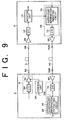
- FIG. 9 is a block diagram showing a preferred embodiment of the system according to the present invention.
- an optical fiber transmission line 64 different from the optical fiber transmission line 6 is used for transmission of supervisory information from the second terminal device 4 to the first terminal device 2. That is, the optical fiber transmission line 6 is used as a downstream line directed from the first terminal device 2 toward the second terminal device 4, and the optical fiber transmission line 64 is used as an upstream line directed from the second terminal device 4 toward the first terminal device 2.
- An optical signal inclusive of the supervisory information output from the transmitting unit 16 in the second terminal device 4 is amplified by an optical amplifier 66 as a postamplifier, and an amplified optical signal output from the optical amplifier 66 is supplied into the optical fiber transmission line 64 from its first end 64A.
- An optical signal output from the second end 64B of the optical fiber transmission line 64 is amplified by an optical amplifier 68 as a preamplifier, and an amplified optical signal output from the optical amplifier 68 is supplied into the receiving unit 18 in the first terminal device 2.
- the transmitting unit 16 includes a supervisory information inserting circuit 70 for inserting supervisory information related to a parameter detected by the monitor unit 14 into a main signal to be transmitted by the upstream line, and an E/O converter 72 for converting an output signal from the circuit 70 into an optical signal.
- a supervisory information inserting circuit 70 for inserting supervisory information related to a parameter detected by the monitor unit 14 into a main signal to be transmitted by the upstream line
- an E/O converter 72 for converting an output signal from the circuit 70 into an optical signal.
- the receiving unit 18 includes an O/E converter 74 for converting an optical signal amplified by the optical amplifier 68 into an electrical signal, and a supervisory information extracting circuit 76 for extracting the supervisory information from the output signal from the O/E converter 74.
- the circuit 76 generates the control signal CS according to the extracted supervisory information.
- the optical power of the optical signal to be output from the optical transmitter 8 in the first terminal device 2 can be controlled to an optimum value according to the supervisory information transmitted by the optical fiber transmission line 64. This control will now be described more specifically.
- the launch power of an optical signal according to the kind of the optical fiber transmission lines 6 and 64 (SMF/DSF) and the transmission distance is set in order to obtain a condition where the optical signal is allowed to pass through each of the optical fiber transmission lines 6 and 64 to some extent. Further, in the case that the combination of an SMF and a DCF is adopted as shown in FIG. 5A, the dispersion of the DCF is also set.
- the optical power of the optical signal to be output from the optical transmitter 8 in the first terminal device 2 is changed to detect a parameter (e.g., bit error rate) related to waveform degradation by the monitor unit 14 in the second terminal device 4.
- a parameter e.g., bit error rate
- supervisory information is obtained according to error information, so that the supervisory information thus obtained is transmitted from the transmitting unit 16 to the receiving unit 18.
- an optimum value of the optical power of the optical signal to be output from the optical transmitter 8 can be obtained from the correspondence between the change in the optical power and the error information. Accordingly, the control signal CS is generated so as to obtain the optimum optical power. In this manner, the optical power of the optical signal to be output from the optical transmitter 8 to the optical fiber transmission line 6 can be maintained always at an optimum value, thus allowing compensation for chromatic dispersion and nonlinearity.
- optical power of the optical signal to be output to the optical fiber transmission line 6 is optimized in this preferred embodiment, the optical power of an optical signal to be output to the optical fiber transmission line 64 may be optimized by reversing the functions of the terminal devices 2 and 4. Such a modification can be made very easily by those skilled in the art, so the description thereof will be omitted herein.
- optical power of the optical signal to be output from the optical transmitter 8 may be adjusted manually according to the method of the present invention rather than by the automatic control using the control unit 10 as in the system shown in FIG. 9.
- FIG. 10 is a block diagram showing another preferred embodiment of the system according to the present invention.
- the system shown in FIG. 10 is characterized in that a plurality of optical repeaters 78(#1) to 78(#N) (N is an integer greater than 1) are arranged along the optical fiber transmission line 6, in contrast to the system shown in FIG. 1 or FIG. 9.
- Each of the optical repeaters 78(#1) to 78(#N) is provided as a linear repeater.
- the linear repeater is a repeater for amplifying a received optical signal in an analog manner, and it is distinguished from a regenerative repeater designed to perform waveform shaping or the like.
- Each of the optical repeaters 78(#1) to 78(#N) has an optical amplifier 80 for amplifying a received optical signal.
- a plurality of optical repeaters 82(#1) to 82(#N) are also arranged along the optical fiber transmission line 64.
- Each of the optical repeaters 82(#1) to 82(#N) has an optical amplifier 84.
- the output level (the optical power of an output optical signal) from each optical amplifier 80 is set (fixed) to a constant value.
- the influence of nonlinearity due to a high output level from each optical amplifier 80 is substantially constant. Accordingly, the optical power of the optical signal to be output from the optical transmitter 8 in the first terminal device 2 can be easily set to an optimum value according to the present invention.
- Each optical amplifier 80 may employ the configuration of the optical amplifier shown in FIG. 6 with the reference voltage Vref set constant.
- the output level of the optical transmitter 8 and the output level of each optical amplifier 80 are set substantially equal to each other. That is, the output levels of the optical transmitter 8 and each optical amplifier 80 are adjusted according to the control signal CS (see FIG. 9).
- the output levels of the optical transmitter 8 and the optical amplifiers 80 are adjusted sequentially from the first terminal device 2 toward the second terminal device 4 or from the second terminal device 4 toward the first terminal device 2.
- each optical amplifier 80 is changed according to the control signal CS. Accordingly, in the case that the optical amplifier shown in FIG. 6 is used as each optical amplifier 80, the reference voltage Vref is adjusted according to the control signal CS.
- control signal CS is required in each of the optical repeaters 78(#1) to 78(#N). Accordingly, it is necessary to transmit specific supervisory information including the control signal CS from the first terminal device 2 to each of the optical repeaters 78(#1) to 78(#N).
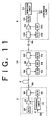
- FIG. 11 is a block diagram showing a modification for transmitting specific supervisory information in the system shown in FIG. 10.
- the first terminal device 2 has an E/O converter 86 for converting specific supervisory information (supervisory signal) generated according to the control signal CS into a supervisory optical signal.
- the supervisory optical signal output from the E/O converter 86 is combined with an optical signal related to a main signal output from the optical transmitter 8 by a WDM (wavelength division multiplexing) coupler 88. Accordingly, the wavelength of the supervisory optical signal is different from the wavelength of the optical signal output from the optical transmitter 8.
- WDM wavelength division multiplexing
- Reference numeral 78 denotes each of the optical repeaters 78(#1) to 78(#N) shown in FIG. 10.
- the supervisory optical signal is extracted by a WDM coupler 90, and the extracted supervisory signal is converted into a supervisory signal by an O/E converter 92.
- the supervisory signal output from the O/E converter 92 is supplied to a supervisory circuit (SV) 94.
- the supervisory circuit 94 adjusts the output level (or gain) of the optical amplifier 80 according to the supervisory signal. For example, in the case that the optical amplifier shown in FIG. 6 is used as the optical amplifier 80, the reference voltage Vref is set according to the supervisory signal.
- the supervisory signal supplied to the supervisory circuit 94 or a supervisory signal updated in the supervisory circuit 94 is converted into a supervisory optical signal by an E/O converter 96.
- the supervisory optical signal output from the E/O converter 96 is supplied to a WDM coupler 98, in which the supervisory optical signal is combined with an optical signal amplified by the optical amplifier 80.
- the supervisory optical signal is extracted by a WDM coupler 100, and the extracted supervisory optical signal is converted into a supervisory signal by an O/E converter 102.
- the supervisory signal output from the O/E converter 102 is supplied to a supervisory circuit 104, and an output signal from the supervisory circuit 104 is fed to the upstream line together with an output signal from the monitor unit 14.
- FIG. 10 A control flow in the system shown in FIG. 10 (FIG. 11) will now be described with reference to FIG. 12 in the case of carrying out the third application form.
- initial information on the transmission lines is input.
- the initial information include the kind of the transmission lines (DSF/SMF/others), the distance of each repeater spacing, the presence/absence of a dispersion compensator, the dispersion in the case that the dispersion compensator is present, and parameters of the transmission lines (loss coefficient, dispersion coefficient, and nonlinear coefficient).
- step 114 the output levels of the optical transmitter 8 and each optical amplifier 80 are initially set according to the input initial information, in order that the optical signal from the first terminal device 2 is transmitted to the second terminal device 4 with a certain level of transmission quality.
- Step 116 optimum detection and setting are started. Step 116 is executed in the order of the downstream line (the optical fiber transmission line 6) and the upstream line (the optical fiber transmission line 64), for example.
- step 118 the optimum detection and setting for each section of the downstream line are carried out.
- the output levels of the optical transmitter 8 and the optical repeaters 78(#1) to 78(#N) are set in this order.
- step 120 it is determined whether or not the setting for all the lines has been finished. If the setting for all the lines has not yet been finished, the program returns to step 116 to start the optimum detection and setting for the upstream line.
- step 122 in which the set information is recorded into a memory device associated with a CPU provided in the first terminal device 2, for example.
- the setting operation by the control flow shown in FIG. 12 is carried out for the downstream line sequentially from the first terminal device 2 toward the second terminal device 4, the setting operation may be carried out in reverse order. Further, the setting operation for the upstream line can also be carried out similarly.
Landscapes
- Physics & Mathematics (AREA)
- Electromagnetism (AREA)
- Engineering & Computer Science (AREA)
- Computer Networks & Wireless Communication (AREA)
- Signal Processing (AREA)
- Optical Communication System (AREA)
- Cable Transmission Systems, Equalization Of Radio And Reduction Of Echo (AREA)
Applications Claiming Priority (2)
| Application Number | Priority Date | Filing Date | Title |
|---|---|---|---|
| JP19253098 | 1998-07-08 | ||
| JP10192530A JP2000031900A (ja) | 1998-07-08 | 1998-07-08 | 光ファイバ通信のための方法並びに該方法の実施に使用する端局装置及びシステム |
Publications (2)
| Publication Number | Publication Date |
|---|---|
| EP0971493A2 true EP0971493A2 (de) | 2000-01-12 |
| EP0971493A3 EP0971493A3 (de) | 2002-09-11 |
Family
ID=16292823
Family Applications (1)
| Application Number | Title | Priority Date | Filing Date |
|---|---|---|---|
| EP99113578A Withdrawn EP0971493A3 (de) | 1998-07-08 | 1999-07-08 | Nichtlinearitäts- und Farbenzerstreuungskompensierung in faseroptischer Übertragung |
Country Status (3)
| Country | Link |
|---|---|
| US (1) | US6738584B1 (de) |
| EP (1) | EP0971493A3 (de) |
| JP (1) | JP2000031900A (de) |
Cited By (17)
| Publication number | Priority date | Publication date | Assignee | Title |
|---|---|---|---|---|
| WO2000052855A1 (de) * | 1999-03-01 | 2000-09-08 | Siemens Aktiengesellschaft | Verfahren und anordnung zur optimierung der impulsform eines amplitudenmodulierten optischen signals |
| WO2001061888A3 (en) * | 2000-02-18 | 2002-05-10 | Corning Inc | Electrical detector for adaptive control of chromatic dispersion in optical systems |
| WO2004032385A1 (en) * | 2002-10-03 | 2004-04-15 | Nortel Networks Limited | Optical dispersion compensation in the electrical domain in an optical communications system |
| WO2004098101A1 (en) * | 2003-04-29 | 2004-11-11 | Draka Comteq Bv | A chromatic dispersion compensation module |
| US6931186B2 (en) | 2002-04-05 | 2005-08-16 | Alcatel | Chromatic dispersion compensation module |
| RU2260249C2 (ru) * | 2003-07-14 | 2005-09-10 | ОАО НПП "Дальняя связь" | Система подводной кабельной глубоководной связи с подводными лодками |
| US7023601B2 (en) | 2002-12-02 | 2006-04-04 | Nortel Networks Limited | Optical E-field modulation using a Mach-Zehnder interferometer |
| EP1422845A3 (de) * | 2002-11-21 | 2006-05-03 | Fujitsu Limited | Verfahren und Vorrichtung zur optischen Dispersionsüberwachung |
| US7200339B1 (en) | 2003-04-11 | 2007-04-03 | Nortel Networks Limited | Method and apparatus for laser line-width compensation |
| US7266306B1 (en) | 2003-10-03 | 2007-09-04 | Nortel Networks Limited | Method for optical carrier suppression and quadrature control |
| US7321734B2 (en) | 2004-07-29 | 2008-01-22 | Nortel Networks Limited | Digital synthesis of readily compensated optical signals |
| US7676161B2 (en) | 2004-12-10 | 2010-03-09 | Nortel Networks Limited | Modulation E-field based control of a non-linear transmitter |
| US7680420B1 (en) | 2003-10-03 | 2010-03-16 | Nortel Networks Limited | Optical E-field modulation using a directly driven laser |
| US7756421B2 (en) | 2002-10-03 | 2010-07-13 | Ciena Corporation | Electrical domain compensation of non-linear effects in an optical communications system |
| US7787778B2 (en) | 2004-12-10 | 2010-08-31 | Ciena Corporation | Control system for a polar optical transmitter |
| US8521040B2 (en) | 2009-12-04 | 2013-08-27 | Electronics And Telecommunications Research Institute | Optical orthogonal frequency division multiplexing receiver and optical signal receiving method thereof |
| CN104009797A (zh) * | 2014-06-10 | 2014-08-27 | 华中科技大学 | 基于数字非线性处理的色散损伤监测方法 |
Families Citing this family (32)
| Publication number | Priority date | Publication date | Assignee | Title |
|---|---|---|---|---|
| GB2366925A (en) * | 2000-09-13 | 2002-03-20 | Marconi Comm Ltd | Power control and equalisation in an optical WDM system |
| US20020131106A1 (en) * | 2001-03-16 | 2002-09-19 | Peter Snawerdt | Secure wave-division multiplexing telecommunications system and method |
| FR2832274B1 (fr) * | 2001-11-15 | 2006-08-25 | Alcatel Optronics | Procede de controle dynamique d'un module optique |
| US20030133652A1 (en) * | 2002-01-15 | 2003-07-17 | Andrekson Peter A. | Method and apparatus for improving performance in noise limited optical transmission systems |
| US7062177B1 (en) * | 2002-06-25 | 2006-06-13 | Cypress Semiconductor Corp. | Out of band communications link for 4-lane optical modules using dark fibers and low-bandwidth LEDs |
| US20040001721A1 (en) * | 2002-06-26 | 2004-01-01 | Lucent Technologies, Inc. | Methods and apparatus for monitoring optical transmissions |
| AU2003288448A1 (en) * | 2002-12-17 | 2004-07-09 | Xyratex Technology Limited | Network tap module |
| JP4553556B2 (ja) | 2003-03-25 | 2010-09-29 | 富士通株式会社 | 波長多重光信号の品質監視方法および装置、並びに、それを用いた光伝送システム |
| US8374508B2 (en) * | 2003-06-12 | 2013-02-12 | Alexander I Soto | Augmenting passive optical networks |
| JP4247834B2 (ja) * | 2004-05-19 | 2009-04-02 | 三菱電機株式会社 | 観測装置及び観測システム |
| EP1610476A1 (de) * | 2004-06-24 | 2005-12-28 | Agilent Technologies Inc | Optische Signallaufzeitmessung |
| US7581891B2 (en) * | 2004-10-15 | 2009-09-01 | Emcore Corporation | Laser adjustment in integrated optoelectronic modules/fiber optic cables |
| US8000607B2 (en) * | 2005-01-25 | 2011-08-16 | Finisar Corporation | Optical transceivers with closed-loop digital diagnostics |
| GB2428149B (en) * | 2005-07-07 | 2009-10-28 | Agilent Technologies Inc | Multimode optical fibre communication system |
| US8160453B1 (en) | 2006-03-30 | 2012-04-17 | Rockstar Bidco, LP | Protection switching with transmitter compensation function |
| US7970288B2 (en) * | 2006-10-30 | 2011-06-28 | Mediatek Inc. | Electronic system with APC |
| US8175191B2 (en) * | 2007-02-20 | 2012-05-08 | Adaptrum, Inc. | Combined sensing methods for cognitive radio |
| JP5471578B2 (ja) * | 2010-02-23 | 2014-04-16 | 富士通株式会社 | 波長分散測定方法および装置、並びに、光伝送システム |
| WO2012006777A1 (en) * | 2010-07-14 | 2012-01-19 | Huawei Technologies Co., Ltd. | Transponder for an optical communications system and optical communications system |
| WO2013162544A1 (en) * | 2012-04-25 | 2013-10-31 | Hewlett-Packard Development Company, L.P. | Operating vertical-cavity surface-emitting lasers |
| JP5994508B2 (ja) * | 2012-09-18 | 2016-09-21 | 富士通株式会社 | 送信装置、通信システム、及び送信レベルの制御方法 |
| CN102914423B (zh) * | 2012-11-01 | 2015-06-03 | 电子科技大学 | 一种色散光纤凹陷频率测量方法 |
| CN105052056B (zh) * | 2013-03-15 | 2018-05-22 | 日本电气株式会社 | 光发射/接收设备、光通信系统、以及光发射/接收方法 |
| JP2015008380A (ja) * | 2013-06-25 | 2015-01-15 | 日立金属株式会社 | 光アクティブケーブルおよび光伝送システム |
| JP2016213729A (ja) * | 2015-05-12 | 2016-12-15 | 富士通株式会社 | 光送信装置および光受信装置 |
| US10298330B2 (en) * | 2016-03-30 | 2019-05-21 | Finisar Corporation | Host-equalized optical inks |
| JP6996559B2 (ja) * | 2017-07-14 | 2022-01-17 | 日本電気株式会社 | プラガブル光モジュール、光通信システム及びプラガブル光モジュールの制御方法 |
| JP7423934B2 (ja) * | 2019-08-16 | 2024-01-30 | ソニーグループ株式会社 | 通信装置、通信方法、及び通信プログラム |
| US11177886B2 (en) * | 2019-11-01 | 2021-11-16 | Ii-Vi Delaware, Inc. | Pluggable optical amplifier for datacenter interconnects |
| KR20220065471A (ko) * | 2020-11-13 | 2022-05-20 | 주식회사 쏠리드 | 광통신 모듈의 광파워 조절 방법 |
| US11575241B2 (en) | 2020-12-11 | 2023-02-07 | Ii-Vi Delaware, Inc. | Optical amplifier modules |
| WO2025177484A1 (ja) * | 2024-02-21 | 2025-08-28 | Ntt株式会社 | 分析装置及び分析方法 |
Family Cites Families (14)
| Publication number | Priority date | Publication date | Assignee | Title |
|---|---|---|---|---|
| JPS6112138A (ja) | 1984-06-27 | 1986-01-20 | Nec Corp | 光フアイバデ−タリンク |
| JPH0834454B2 (ja) | 1990-03-01 | 1996-03-29 | 国際電信電話株式会社 | 光中継器の監視方式 |
| JPH05327625A (ja) | 1992-05-15 | 1993-12-10 | Hitachi Ltd | 光伝送方式 |
| US5343320A (en) * | 1992-08-03 | 1994-08-30 | At&T Bell Laboratories | Pump laser control circuit for an optical transmission system |
| JP3195160B2 (ja) * | 1994-05-06 | 2001-08-06 | 株式会社日立製作所 | 光増幅器 |
| EP0684709B1 (de) * | 1994-05-25 | 2002-10-02 | AT&T Corp. | Optisches Übertragungssystem mit verstellbarer Dispersionskompensation |
| JP2661574B2 (ja) * | 1994-12-28 | 1997-10-08 | 日本電気株式会社 | Ln変調器直流バイアス回路 |
| US5760940A (en) * | 1995-10-27 | 1998-06-02 | Lucent Technologies Inc. | Methods for monitoring optical path characteristics in an optical communication system |
| GB2315938B (en) * | 1996-08-01 | 2001-02-28 | Northern Telecom Ltd | Optical transmission system fault analysis |
| JPH1065627A (ja) * | 1996-08-20 | 1998-03-06 | Fujitsu Ltd | 光送信機、光通信システム及び光通信方法 |
| JPH1188260A (ja) * | 1997-09-09 | 1999-03-30 | Fujitsu Ltd | 光伝送路の分散補償装置 |
| JPH11122173A (ja) * | 1997-10-20 | 1999-04-30 | Fujitsu Ltd | 波長分散による波形変化の検出及びその補償のための方法と装置 |
| US6115157A (en) * | 1997-12-24 | 2000-09-05 | Nortel Networks Corporation | Methods for equalizing WDM systems |
| US6157477A (en) * | 1998-05-27 | 2000-12-05 | Mci Communications Corporations | Bidirectional dispersion compensation system |
-
1998
- 1998-07-08 JP JP10192530A patent/JP2000031900A/ja not_active Withdrawn
-
1999
- 1999-07-08 EP EP99113578A patent/EP0971493A3/de not_active Withdrawn
- 1999-07-08 US US09/349,446 patent/US6738584B1/en not_active Expired - Lifetime
Cited By (29)
| Publication number | Priority date | Publication date | Assignee | Title |
|---|---|---|---|---|
| US7103286B1 (en) | 1999-03-01 | 2006-09-05 | Siemens Aktiengesellschaft | Method and system for optimizing the pulse form of an amplitude modulated optical signal |
| WO2000052855A1 (de) * | 1999-03-01 | 2000-09-08 | Siemens Aktiengesellschaft | Verfahren und anordnung zur optimierung der impulsform eines amplitudenmodulierten optischen signals |
| WO2001061888A3 (en) * | 2000-02-18 | 2002-05-10 | Corning Inc | Electrical detector for adaptive control of chromatic dispersion in optical systems |
| US6487352B1 (en) | 2000-02-18 | 2002-11-26 | Corning Incorporated | Electrical detector for adaptive control of chromatic dispersion in optical systems |
| US6498886B1 (en) | 2000-02-18 | 2002-12-24 | Corning, Incorporated | Adaptive feedback control method for polarization mode dispersion or chromatic dispersion compensation |
| US6931186B2 (en) | 2002-04-05 | 2005-08-16 | Alcatel | Chromatic dispersion compensation module |
| US7376358B2 (en) | 2002-10-03 | 2008-05-20 | Nortel Networks Limited | Location specific optical monitoring |
| US10164707B2 (en) | 2002-10-03 | 2018-12-25 | Ciena Corporation | Optical dispersion compensation in the electrical domain in an optical communications system |
| US7756421B2 (en) | 2002-10-03 | 2010-07-13 | Ciena Corporation | Electrical domain compensation of non-linear effects in an optical communications system |
| EP3211809A1 (de) * | 2002-10-03 | 2017-08-30 | Ciena Luxembourg S.a.r.l. | Optische dispersionskompensation im elektrischen bereich in einem optischen kommunikationssystem |
| WO2004032385A1 (en) * | 2002-10-03 | 2004-04-15 | Nortel Networks Limited | Optical dispersion compensation in the electrical domain in an optical communications system |
| US9853725B2 (en) | 2002-10-03 | 2017-12-26 | Ciena Corporation | Optical dispersion compensation in the electrical domain in an optical communications system |
| US10574352B2 (en) | 2002-10-03 | 2020-02-25 | Ciena Corporation | Compensation of transmitter or receiver defects in an optical communications system |
| US7382984B2 (en) | 2002-10-03 | 2008-06-03 | Nortel Networks Limited | Electrical domain compensation of optical dispersion in an optical communications system |
| US9559778B2 (en) | 2002-10-03 | 2017-01-31 | Ciena Corporation | Optical dispersion compensation in the electrical domain in an optical communications system |
| US7324758B2 (en) | 2002-11-21 | 2008-01-29 | Fujitsu Limited | Optical dispersion monitoring apparatus and optical dispersion monitoring method, and optical transmission system using same |
| EP1422845A3 (de) * | 2002-11-21 | 2006-05-03 | Fujitsu Limited | Verfahren und Vorrichtung zur optischen Dispersionsüberwachung |
| US7023601B2 (en) | 2002-12-02 | 2006-04-04 | Nortel Networks Limited | Optical E-field modulation using a Mach-Zehnder interferometer |
| US7200339B1 (en) | 2003-04-11 | 2007-04-03 | Nortel Networks Limited | Method and apparatus for laser line-width compensation |
| WO2004098101A1 (en) * | 2003-04-29 | 2004-11-11 | Draka Comteq Bv | A chromatic dispersion compensation module |
| RU2260249C2 (ru) * | 2003-07-14 | 2005-09-10 | ОАО НПП "Дальняя связь" | Система подводной кабельной глубоководной связи с подводными лодками |
| US7680420B1 (en) | 2003-10-03 | 2010-03-16 | Nortel Networks Limited | Optical E-field modulation using a directly driven laser |
| US7266306B1 (en) | 2003-10-03 | 2007-09-04 | Nortel Networks Limited | Method for optical carrier suppression and quadrature control |
| US7321734B2 (en) | 2004-07-29 | 2008-01-22 | Nortel Networks Limited | Digital synthesis of readily compensated optical signals |
| US7787778B2 (en) | 2004-12-10 | 2010-08-31 | Ciena Corporation | Control system for a polar optical transmitter |
| US7676161B2 (en) | 2004-12-10 | 2010-03-09 | Nortel Networks Limited | Modulation E-field based control of a non-linear transmitter |
| US8521040B2 (en) | 2009-12-04 | 2013-08-27 | Electronics And Telecommunications Research Institute | Optical orthogonal frequency division multiplexing receiver and optical signal receiving method thereof |
| CN104009797A (zh) * | 2014-06-10 | 2014-08-27 | 华中科技大学 | 基于数字非线性处理的色散损伤监测方法 |
| CN104009797B (zh) * | 2014-06-10 | 2017-10-13 | 华中科技大学 | 基于数字非线性处理的色散损伤监测方法 |
Also Published As
| Publication number | Publication date |
|---|---|
| US6738584B1 (en) | 2004-05-18 |
| JP2000031900A (ja) | 2000-01-28 |
| EP0971493A3 (de) | 2002-09-11 |
Similar Documents
| Publication | Publication Date | Title |
|---|---|---|
| US6738584B1 (en) | Method for optical fiber communication, and terminal device and system for use in carrying out the method | |
| US7006769B1 (en) | Method for optical fiber communication, and device and system for use in carrying out the method | |
| US6038356A (en) | Lightwave transmission system employing raman and rare-earth doped fiber amplification | |
| US7116918B2 (en) | Optical transmission system using in-line amplifiers | |
| US5539563A (en) | System and method for simultaneously compensating for chromatic dispersion and self phase modulation in optical fibers | |
| EP1168530B1 (de) | Ramanverstärker | |
| US6191854B1 (en) | Optical telecommunications system | |
| US5675428A (en) | Optical communication apparatus | |
| EP0897205A2 (de) | Verfahren und Vorrichtung zur optischen Verstärkung und System das solche Vorrichtung verwendet | |
| EP1461877B1 (de) | Optisches übertragungssystem mit raman-verstärkern und einem überwachungssystem | |
| US7558480B2 (en) | Unrepeatered optical communication system with suppressed SBS | |
| US6823107B2 (en) | Method and device for optical amplification | |
| JPWO2005114317A1 (ja) | ラマン増幅用光ファイバ、光ファイバコイル、ラマン増幅器及び光通信システム | |
| US6031659A (en) | Optical amplifier for wavelength-division multiplexing | |
| CA2366039A1 (en) | Optical amplifier, optical communication system including the same, and optical fiber module included in the same | |
| US8538218B2 (en) | Unrepeatered long haul optical fiber transmission systems | |
| US6909535B2 (en) | Optical communication system employing raman amplification | |
| US6876488B1 (en) | Discrete amplification of an optical signal | |
| EP1802006B1 (de) | Vorrichtung und Verfahren zur automatischen Abstimmung einer Farbzerstreuungskompensation für WDM Übertragungssysteme unter Verwendung einer verteilten Raman Co-Pumpe | |
| CN1240944A (zh) | 光纤通信的方法和供此方法使用的终端装置和系统 | |
| Tomkos et al. | Transmission of 1550nm 10Gb/s directly modulated signal over 100km of negative dispersion fiber without any dispersion compensation | |
| JP2732746B2 (ja) | 光増幅器の入出力光パワーのモニタ方法 | |
| JP4626309B2 (ja) | 信号品質情報装置、信号品質評価方法、光信号評価システムおよび光伝送システム | |
| EP0887956B1 (de) | Optisches Übertragungssystem mit Farbzerstreuungskompensator | |
| JPH05327625A (ja) | 光伝送方式 |
Legal Events
| Date | Code | Title | Description |
|---|---|---|---|
| PUAI | Public reference made under article 153(3) epc to a published international application that has entered the european phase |
Free format text: ORIGINAL CODE: 0009012 |
|
| AK | Designated contracting states |
Kind code of ref document: A2 Designated state(s): AT BE CH CY DE DK ES FI FR GB GR IE IT LI LU MC NL PT SE |
|
| AX | Request for extension of the european patent |
Free format text: AL;LT;LV;MK;RO;SI |
|
| RIN1 | Information on inventor provided before grant (corrected) |
Inventor name: OKANO, SATORU Inventor name: KAWASAKI, YUMIKO Inventor name: YAMANE, KAZUO Inventor name: TSUDA, TAKASHI |
|
| PUAL | Search report despatched |
Free format text: ORIGINAL CODE: 0009013 |
|
| AK | Designated contracting states |
Kind code of ref document: A3 Designated state(s): AT BE CH CY DE DK ES FI FR GB GR IE IT LI LU MC NL PT SE |
|
| AX | Request for extension of the european patent |
Free format text: AL;LT;LV;MK;RO;SI |
|
| 17P | Request for examination filed |
Effective date: 20020911 |
|
| 17Q | First examination report despatched |
Effective date: 20021113 |
|
| AKX | Designation fees paid |
Designated state(s): DE FR GB |
|
| GRAH | Despatch of communication of intention to grant a patent |
Free format text: ORIGINAL CODE: EPIDOS IGRA |
|
| STAA | Information on the status of an ep patent application or granted ep patent |
Free format text: STATUS: THE APPLICATION IS DEEMED TO BE WITHDRAWN |
|
| 18D | Application deemed to be withdrawn |
Effective date: 20031111 |