EP0971561B1 - Résistance électrique chauffante pour four électrique et procédé de fabrication d'une telle résistance - Google Patents
Résistance électrique chauffante pour four électrique et procédé de fabrication d'une telle résistance Download PDFInfo
- Publication number
- EP0971561B1 EP0971561B1 EP99401460A EP99401460A EP0971561B1 EP 0971561 B1 EP0971561 B1 EP 0971561B1 EP 99401460 A EP99401460 A EP 99401460A EP 99401460 A EP99401460 A EP 99401460A EP 0971561 B1 EP0971561 B1 EP 0971561B1
- Authority
- EP
- European Patent Office
- Prior art keywords
- particles
- resistance
- silicon carbide
- heating
- doping
- Prior art date
- Legal status (The legal status is an assumption and is not a legal conclusion. Google has not performed a legal analysis and makes no representation as to the accuracy of the status listed.)
- Expired - Lifetime
Links
- 238000010438 heat treatment Methods 0.000 title claims abstract description 33
- 238000004519 manufacturing process Methods 0.000 title claims description 10
- 239000002245 particle Substances 0.000 claims abstract description 57
- HBMJWWWQQXIZIP-UHFFFAOYSA-N silicon carbide Chemical compound [Si+]#[C-] HBMJWWWQQXIZIP-UHFFFAOYSA-N 0.000 claims abstract description 27
- 229910010271 silicon carbide Inorganic materials 0.000 claims abstract description 27
- 239000000203 mixture Substances 0.000 claims abstract description 23
- 229910052500 inorganic mineral Inorganic materials 0.000 claims abstract description 16
- 239000011707 mineral Substances 0.000 claims abstract description 16
- 229910000480 nickel oxide Inorganic materials 0.000 claims abstract description 9
- GNRSAWUEBMWBQH-UHFFFAOYSA-N oxonickel Chemical compound [Ni]=O GNRSAWUEBMWBQH-UHFFFAOYSA-N 0.000 claims abstract description 9
- PNEYBMLMFCGWSK-UHFFFAOYSA-N aluminium oxide Inorganic materials [O-2].[O-2].[O-2].[Al+3].[Al+3] PNEYBMLMFCGWSK-UHFFFAOYSA-N 0.000 claims abstract description 7
- SIWVEOZUMHYXCS-UHFFFAOYSA-N oxo(oxoyttriooxy)yttrium Chemical compound O=[Y]O[Y]=O SIWVEOZUMHYXCS-UHFFFAOYSA-N 0.000 claims abstract description 7
- 238000005245 sintering Methods 0.000 claims description 15
- 229910010293 ceramic material Inorganic materials 0.000 claims description 9
- 238000000034 method Methods 0.000 claims description 7
- 238000001125 extrusion Methods 0.000 claims description 6
- 239000011368 organic material Substances 0.000 claims description 5
- 238000007493 shaping process Methods 0.000 claims description 5
- 238000002360 preparation method Methods 0.000 claims description 3
- 230000001050 lubricating effect Effects 0.000 claims description 2
- 239000004014 plasticizer Substances 0.000 claims description 2
- 238000007669 thermal treatment Methods 0.000 claims 1
- 239000002019 doping agent Substances 0.000 abstract 2
- 239000000919 ceramic Substances 0.000 abstract 1
- 239000012071 phase Substances 0.000 description 14
- XUIMIQQOPSSXEZ-UHFFFAOYSA-N Silicon Chemical compound [Si] XUIMIQQOPSSXEZ-UHFFFAOYSA-N 0.000 description 6
- PXHVJJICTQNCMI-UHFFFAOYSA-N Nickel Chemical compound [Ni] PXHVJJICTQNCMI-UHFFFAOYSA-N 0.000 description 5
- 239000000470 constituent Substances 0.000 description 4
- 238000005485 electric heating Methods 0.000 description 4
- 229920000609 methyl cellulose Polymers 0.000 description 4
- 239000001923 methylcellulose Substances 0.000 description 4
- 230000003647 oxidation Effects 0.000 description 4
- 238000007254 oxidation reaction Methods 0.000 description 4
- QVGXLLKOCUKJST-UHFFFAOYSA-N atomic oxygen Chemical compound [O] QVGXLLKOCUKJST-UHFFFAOYSA-N 0.000 description 3
- 229910052759 nickel Inorganic materials 0.000 description 3
- 239000001301 oxygen Substances 0.000 description 3
- 229910052760 oxygen Inorganic materials 0.000 description 3
- WRIDQFICGBMAFQ-UHFFFAOYSA-N (E)-8-Octadecenoic acid Natural products CCCCCCCCCC=CCCCCCCC(O)=O WRIDQFICGBMAFQ-UHFFFAOYSA-N 0.000 description 2
- LQJBNNIYVWPHFW-UHFFFAOYSA-N 20:1omega9c fatty acid Natural products CCCCCCCCCCC=CCCCCCCCC(O)=O LQJBNNIYVWPHFW-UHFFFAOYSA-N 0.000 description 2
- QSBYPNXLFMSGKH-UHFFFAOYSA-N 9-Heptadecensaeure Natural products CCCCCCCC=CCCCCCCCC(O)=O QSBYPNXLFMSGKH-UHFFFAOYSA-N 0.000 description 2
- 229910018072 Al 2 O 3 Inorganic materials 0.000 description 2
- XKRFYHLGVUSROY-UHFFFAOYSA-N Argon Chemical compound [Ar] XKRFYHLGVUSROY-UHFFFAOYSA-N 0.000 description 2
- IJGRMHOSHXDMSA-UHFFFAOYSA-N Atomic nitrogen Chemical compound N#N IJGRMHOSHXDMSA-UHFFFAOYSA-N 0.000 description 2
- ZQPPMHVWECSIRJ-UHFFFAOYSA-N Oleic acid Natural products CCCCCCCCC=CCCCCCCCC(O)=O ZQPPMHVWECSIRJ-UHFFFAOYSA-N 0.000 description 2
- 239000005642 Oleic acid Substances 0.000 description 2
- 239000004264 Petrolatum Substances 0.000 description 2
- 239000000654 additive Substances 0.000 description 2
- HIGRAKVNKLCVCA-UHFFFAOYSA-N alumine Chemical compound C1=CC=[Al]C=C1 HIGRAKVNKLCVCA-UHFFFAOYSA-N 0.000 description 2
- 238000009826 distribution Methods 0.000 description 2
- QXJSBBXBKPUZAA-UHFFFAOYSA-N isooleic acid Natural products CCCCCCCC=CCCCCCCCCC(O)=O QXJSBBXBKPUZAA-UHFFFAOYSA-N 0.000 description 2
- 239000007791 liquid phase Substances 0.000 description 2
- 238000003754 machining Methods 0.000 description 2
- ZQPPMHVWECSIRJ-KTKRTIGZSA-N oleic acid Chemical compound CCCCCCCC\C=C/CCCCCCCC(O)=O ZQPPMHVWECSIRJ-KTKRTIGZSA-N 0.000 description 2
- 229940066842 petrolatum Drugs 0.000 description 2
- 235000019271 petrolatum Nutrition 0.000 description 2
- 239000000843 powder Substances 0.000 description 2
- PYWVYCXTNDRMGF-UHFFFAOYSA-N rhodamine B Chemical compound [Cl-].C=12C=CC(=[N+](CC)CC)C=C2OC2=CC(N(CC)CC)=CC=C2C=1C1=CC=CC=C1C(O)=O PYWVYCXTNDRMGF-UHFFFAOYSA-N 0.000 description 2
- 239000010703 silicon Substances 0.000 description 2
- 229910052710 silicon Inorganic materials 0.000 description 2
- 239000002904 solvent Substances 0.000 description 2
- 229910052727 yttrium Inorganic materials 0.000 description 2
- VWQVUPCCIRVNHF-UHFFFAOYSA-N yttrium atom Chemical compound [Y] VWQVUPCCIRVNHF-UHFFFAOYSA-N 0.000 description 2
- 206010063493 Premature ageing Diseases 0.000 description 1
- 208000032038 Premature aging Diseases 0.000 description 1
- 229910004298 SiO 2 Inorganic materials 0.000 description 1
- JNDMLEXHDPKVFC-UHFFFAOYSA-N aluminum;oxygen(2-);yttrium(3+) Chemical compound [O-2].[O-2].[O-2].[Al+3].[Y+3] JNDMLEXHDPKVFC-UHFFFAOYSA-N 0.000 description 1
- 239000012080 ambient air Substances 0.000 description 1
- 150000001412 amines Chemical class 0.000 description 1
- 229910052786 argon Inorganic materials 0.000 description 1
- 238000000889 atomisation Methods 0.000 description 1
- 230000003416 augmentation Effects 0.000 description 1
- 239000011230 binding agent Substances 0.000 description 1
- 230000015572 biosynthetic process Effects 0.000 description 1
- 238000006243 chemical reaction Methods 0.000 description 1
- 238000010411 cooking Methods 0.000 description 1
- 238000005260 corrosion Methods 0.000 description 1
- 230000007797 corrosion Effects 0.000 description 1
- 238000009792 diffusion process Methods 0.000 description 1
- 230000008030 elimination Effects 0.000 description 1
- 238000003379 elimination reaction Methods 0.000 description 1
- 238000001704 evaporation Methods 0.000 description 1
- 230000008020 evaporation Effects 0.000 description 1
- 239000007789 gas Substances 0.000 description 1
- 238000000265 homogenisation Methods 0.000 description 1
- 238000002955 isolation Methods 0.000 description 1
- 239000007788 liquid Substances 0.000 description 1
- 239000000314 lubricant Substances 0.000 description 1
- 239000000463 material Substances 0.000 description 1
- 238000002156 mixing Methods 0.000 description 1
- 230000007935 neutral effect Effects 0.000 description 1
- 229910052757 nitrogen Inorganic materials 0.000 description 1
- 239000003921 oil Substances 0.000 description 1
- 239000005416 organic matter Substances 0.000 description 1
- 230000001590 oxidative effect Effects 0.000 description 1
- 239000012466 permeate Substances 0.000 description 1
- 239000000047 product Substances 0.000 description 1
- 239000002994 raw material Substances 0.000 description 1
- 229910019655 synthetic inorganic crystalline material Inorganic materials 0.000 description 1
- 229940099259 vaseline Drugs 0.000 description 1
- 238000003466 welding Methods 0.000 description 1
- 229910019901 yttrium aluminum garnet Inorganic materials 0.000 description 1
Images
Classifications
-
- H—ELECTRICITY
- H05—ELECTRIC TECHNIQUES NOT OTHERWISE PROVIDED FOR
- H05B—ELECTRIC HEATING; ELECTRIC LIGHT SOURCES NOT OTHERWISE PROVIDED FOR; CIRCUIT ARRANGEMENTS FOR ELECTRIC LIGHT SOURCES, IN GENERAL
- H05B3/00—Ohmic-resistance heating
- H05B3/10—Heating elements characterised by the composition or nature of the materials or by the arrangement of the conductor
- H05B3/12—Heating elements characterised by the composition or nature of the materials or by the arrangement of the conductor characterised by the composition or nature of the conductive material
- H05B3/14—Heating elements characterised by the composition or nature of the materials or by the arrangement of the conductor characterised by the composition or nature of the conductive material the material being non-metallic
- H05B3/141—Conductive ceramics, e.g. metal oxides, metal carbides, barium titanate, ferrites, zirconia, vitrous compounds
-
- H—ELECTRICITY
- H05—ELECTRIC TECHNIQUES NOT OTHERWISE PROVIDED FOR
- H05B—ELECTRIC HEATING; ELECTRIC LIGHT SOURCES NOT OTHERWISE PROVIDED FOR; CIRCUIT ARRANGEMENTS FOR ELECTRIC LIGHT SOURCES, IN GENERAL
- H05B3/00—Ohmic-resistance heating
- H05B3/10—Heating elements characterised by the composition or nature of the materials or by the arrangement of the conductor
- H05B3/12—Heating elements characterised by the composition or nature of the materials or by the arrangement of the conductor characterised by the composition or nature of the conductive material
- H05B3/14—Heating elements characterised by the composition or nature of the materials or by the arrangement of the conductor characterised by the composition or nature of the conductive material the material being non-metallic
- H05B3/148—Silicon, e.g. silicon carbide, magnesium silicide, heating transistors or diodes
-
- H—ELECTRICITY
- H05—ELECTRIC TECHNIQUES NOT OTHERWISE PROVIDED FOR
- H05B—ELECTRIC HEATING; ELECTRIC LIGHT SOURCES NOT OTHERWISE PROVIDED FOR; CIRCUIT ARRANGEMENTS FOR ELECTRIC LIGHT SOURCES, IN GENERAL
- H05B3/00—Ohmic-resistance heating
- H05B3/62—Heating elements specially adapted for furnaces
- H05B3/64—Heating elements specially adapted for furnaces using ribbon, rod, or wire heater
Definitions
- the present invention relates to an electrical resistance heater for electric oven, as well as a method of manufacturing such a resistance.
- the electric heating resistors are for example produced by sintering particles of ceramic material, and in particular grains of silicon carbide.
- Silicon carbide which is widely used in the manufacture of such heating elements provides relatively robust resistors with excellent thermal properties.
- Document FR-A-2 757 736 describes an electric heating resistor comprising a resistive body made of silicon carbide and comprising a layer of (Al 2 O 3 + SiO 2 ) protecting against corrosion.
- the premature aging of such resistance is also due to the nature elements added to silicon carbide which generate, at high temperature, a secondary phase of low viscosity. The diffusion of oxygen towards the core of the material can then easily occur and cause oxidation of the heating element.
- the object of the invention is to overcome these drawbacks.
- an electric heating resistance for an oven electric comprising a heating resistive part in ceramic material, characterized in that the ceramic material comprises a sintered mixture of carbide particles of silicon, doping particles suitable for obtaining, after sintering; of a phase electrically conductive and mineral particles.
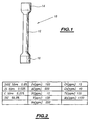
- FIG 1 there is shown a conforming electrical resistance heater to the invention, designated by the general reference 10.
- the resistance shown in this figure has a generally cylindrical shape, however, the invention also applies to the manufacture of heating resistors of any shape, in particular to tubular, straight or bent resistors.
- the resistor 10 essentially comprises a heating body 12 provided with a or two (as shown) mutually opposite end zones 14 and 16 forming mechanical fixing and electrical connection terminals.
- Terminals 14 and 16 have lower resistance than the body heating 12 and are either formed by machining the body, or produced by adding a cylinder on one or on each end of the body 12 and welding thereon.
- Resistor 10 is produced by sintering a ceramic material.
- the resistive part 12 comprises a sintered mixture of silicon carbide particles, doping particles suitable for obtaining a electrically conductive phase, consisting of nickel oxide, and particles minerals allowing liquid sintering of silicon carbide elements, by example of alumina and yttrium oxide.
- the silicon carbide particles In order to improve the density of the resistance, and therefore to decrease its porosity, the silicon carbide particles have a size between 0.1 micron and 20 microns, preferably equal to 1.5 microns.
- particles of silicon carbide constitute two populations whose size distributions are centered on 1 ⁇ m and 10 ⁇ m, respectively, the size distribution of the nickel oxide particles being centered on 0.5 ⁇ m.
- these particles of silicon carbide consist of commercial silicon carbide, for example of the FCP type, sold by "NORTON", USA, in powder form, the composition of which is illustrated in the table shown in the figure 2.
- the electrical connection and mechanical fixing terminals 14 and 16 of the resistance 10 also consist of a sintered mixture of carbide particles of silicon and mineral particles, identical to the particles entering into the constitution of the heating resistive part 12 and comprise a concentration of doping particles leading to a conductive electrical phase greater than that of the heating part.
- terminals 14 and 16 As a variant, and as visible in FIG. 1, it is possible to form the terminals 14 and 16, as described below, forming these during the manufacturing the heating part 12, by providing end zones having a cross-section of dimension larger than that of the resistive part heater 12, either obtained by machining the middle part of the resistor so as to reduce its cross-section, either as mentioned previously, reported on the extremities of the body 12.
- the first step consists of a raw material preparation step.
- NORTON FCP powder additives consisting of particles of mineral matter, namely alumina, Al 2 O 3 , and yttrium oxide Y 2 O 3 , and doping particles, namely nickel oxide NiO, leading to an electrically conductive phase.
- the mixture thus formed is then dried by passage in an oven at 80 ° C. or by atomization, until complete evaporation of the solvent,
- the resistance is shaped into using an extrusion technique.
- organic constituents are used so as to form a dough with rheological characteristics compatible with deformation during passage through a nozzle of an extruder and good mechanical strength of the elements extruded before cooking.
- the organic constituents comprise, previously prepared in the form gel, for example methylcellulose binder, a plasticizer, for example petrolatum as well as lubricants, for example an amine and oleic acid, and are incorporated into the mixture consisting of silicon carbide, mineral particles and doping particles during a mixing step, maintained for example during one o'clock.
- a plasticizer for example petrolatum as well as lubricants, for example an amine and oleic acid
- the dough is then extruded, using an extruder, so as to form cylindrical bars.
- the next manufacturing phase begins with a first processing step thermal aimed at the elimination of organic constituents.
- the bars are placed under ambient air, and a first rise from 20 ° C to 150 ° C using a speed of 30 ° C per hour, then maintains a one hour plateau at this temperature. Then we climb temperature from 150 ° C to 300 ° C, also using a speed of 30 ° C per hour, then this temperature is maintained at 300 ° C for one hour. A third climb in temperature is carried out so as to bring the bars to a temperature of 450 ° C., in using a speed of 30 ° C per hour. We keep the bars at the latter temperature for one hour, then allowed to cool to room temperature.
- the bars thus obtained are then introduced into another oven to undergo the final sintering heat treatment proper.
- Sintering is carried out on the one hand, under vacuum, by raising the temperature by 20 ° C. at 900 ° C, using a speed of 300 ° C per hour, then, under argon, at a pressure of a bar, by raising the temperature from 900 ° C to 2000 ° C, using a speed of 300 ° C per hour, maintaining a two-hour plateau at 2000 ° C, and finally, leaving the resistor will cool down to room temperature.
- Another neutral gas, for nitrogen, for example, can also be used.
- the part heater 12 is extended, on at least one of its ends, by a terminal 14 and 16, of electrical connection and mechanical fixing is added by adding a cylinder on the end of the bars, welded to the heating resistive part 12, or machined after extrusion, is formed simultaneously during the same extrusion step, in providing corresponding end zones having a cross section larger than those of the heating part 12.
- connection terminals 14 and 16 are it is possible to form the added part (s) using a concentration of doping particles leading to an electrically conductive phase higher than that of the heating resistive part 12.
Landscapes
- Chemical & Material Sciences (AREA)
- Engineering & Computer Science (AREA)
- Ceramic Engineering (AREA)
- Resistance Heating (AREA)
- Apparatuses And Processes For Manufacturing Resistors (AREA)
- Non-Adjustable Resistors (AREA)
- Ceramic Products (AREA)
- Furnace Details (AREA)
- Electronic Switches (AREA)
- Conductive Materials (AREA)
Applications Claiming Priority (2)
| Application Number | Priority Date | Filing Date | Title |
|---|---|---|---|
| FR9808634 | 1998-07-06 | ||
| FR9808634A FR2780845B1 (fr) | 1998-07-06 | 1998-07-06 | Resistance electrique chauffante pour four electrique et procede de fabrication d'une telle resistance |
Publications (2)
| Publication Number | Publication Date |
|---|---|
| EP0971561A1 EP0971561A1 (fr) | 2000-01-12 |
| EP0971561B1 true EP0971561B1 (fr) | 2002-09-11 |
Family
ID=9528315
Family Applications (1)
| Application Number | Title | Priority Date | Filing Date |
|---|---|---|---|
| EP99401460A Expired - Lifetime EP0971561B1 (fr) | 1998-07-06 | 1999-06-14 | Résistance électrique chauffante pour four électrique et procédé de fabrication d'une telle résistance |
Country Status (11)
| Country | Link |
|---|---|
| US (1) | US6146550A (da) |
| EP (1) | EP0971561B1 (da) |
| JP (1) | JP2000036371A (da) |
| AT (1) | ATE224127T1 (da) |
| CA (1) | CA2276678A1 (da) |
| DE (1) | DE69902853T2 (da) |
| DK (1) | DK0971561T3 (da) |
| ES (1) | ES2183491T3 (da) |
| FR (1) | FR2780845B1 (da) |
| NO (1) | NO993306L (da) |
| PT (1) | PT971561E (da) |
Families Citing this family (9)
| Publication number | Priority date | Publication date | Assignee | Title |
|---|---|---|---|---|
| US6616890B2 (en) * | 2001-06-15 | 2003-09-09 | Harvest Precision Components, Inc. | Fabrication of an electrically conductive silicon carbide article |
| KR100474333B1 (ko) * | 2002-04-09 | 2005-03-08 | 엘지전자 주식회사 | 전열기의 발열체 단자 구조 |
| EP2610570B1 (en) * | 2011-12-29 | 2016-11-23 | Ipsen, Inc. | Heating element arrangement for a vacuum heat treating furnace |
| KR102137032B1 (ko) | 2017-05-10 | 2020-07-23 | 엘지전자 주식회사 | 탄소 복합체 조성물 및 이를 이용하여 제조되는 탄소 히터 |
| KR102004035B1 (ko) * | 2017-05-26 | 2019-07-25 | 엘지전자 주식회사 | 탄소 발열체 |
| US11342484B2 (en) | 2020-05-11 | 2022-05-24 | Silanna UV Technologies Pte Ltd | Metal oxide semiconductor-based light emitting device |
| EP4423325A4 (en) | 2021-10-27 | 2025-08-27 | Silanna UV Technologies Pte Ltd | METHODS AND SYSTEMS FOR HEATING A WIDE BANDGAP SUBSTRATE |
| JP7814510B2 (ja) | 2021-11-10 | 2026-02-16 | シランナ・ユー・ブイ・テクノロジーズ・プライベート・リミテッド | エピタキシャル酸化物材料、構造、及びデバイス |
| JP7829033B2 (ja) | 2021-11-10 | 2026-03-12 | シランナ・ユー・ブイ・テクノロジーズ・プライベート・リミテッド | 酸化マグネシウムゲルマニウムを含む超ワイドバンドギャップ半導体デバイス |
Family Cites Families (9)
| Publication number | Priority date | Publication date | Assignee | Title |
|---|---|---|---|---|
| US4174971A (en) * | 1975-12-11 | 1979-11-20 | Bulten-Kanthal Aktiebolag | Silicon carbide body containing a molybdenum disilicide alloy |
| JPS6027653A (ja) * | 1983-07-21 | 1985-02-12 | 株式会社日立製作所 | セラミツク抵抗材料 |
| CA1240710A (en) * | 1984-11-08 | 1988-08-16 | Malcolm E. Washburn | Refractory composition and products resulting therefrom |
| GB2170511B (en) * | 1984-12-17 | 1989-06-07 | Toshiba Ceramics Co | Sintered body of silicon carbide |
| SU1636400A1 (ru) * | 1989-04-03 | 1991-03-23 | Днепропетровский государственный университет им.300-летия воссоединения Украины с Россией | Шихта дл изготовлени электронагревателей |
| SU1685752A1 (ru) * | 1989-05-29 | 1991-10-23 | Тернопольский Государственный Педагогический Институт Им.Я.А.Галана | Покрытие дл карбидокремниевых электронагревателей |
| JPH0760730B2 (ja) * | 1991-08-20 | 1995-06-28 | 日本ピラー工業株式会社 | セラミック製ヒーター |
| CZ172294A3 (en) * | 1992-01-16 | 1995-05-17 | Univ Cincinnati | Mixture for preparing composite materials, process for preparing ceramic composite articles, electric heating element and the ceramic composite article |
| FR2757736B1 (fr) * | 1996-12-24 | 1999-01-15 | Electricite De France | Resistance electrique chauffante a longevite amelioree et procede de revetement d'une resistance electrique chauffante |
-
1998
- 1998-07-06 FR FR9808634A patent/FR2780845B1/fr not_active Expired - Fee Related
-
1999
- 1999-06-14 PT PT99401460T patent/PT971561E/pt unknown
- 1999-06-14 EP EP99401460A patent/EP0971561B1/fr not_active Expired - Lifetime
- 1999-06-14 AT AT99401460T patent/ATE224127T1/de not_active IP Right Cessation
- 1999-06-14 DE DE69902853T patent/DE69902853T2/de not_active Expired - Fee Related
- 1999-06-14 DK DK99401460T patent/DK0971561T3/da active
- 1999-06-14 ES ES99401460T patent/ES2183491T3/es not_active Expired - Lifetime
- 1999-06-30 CA CA002276678A patent/CA2276678A1/en not_active Abandoned
- 1999-06-30 US US09/343,204 patent/US6146550A/en not_active Expired - Fee Related
- 1999-07-02 NO NO993306A patent/NO993306L/no not_active Application Discontinuation
- 1999-07-05 JP JP11190140A patent/JP2000036371A/ja active Pending
Also Published As
| Publication number | Publication date |
|---|---|
| NO993306D0 (no) | 1999-07-02 |
| NO993306L (no) | 2000-01-07 |
| CA2276678A1 (en) | 2000-01-06 |
| JP2000036371A (ja) | 2000-02-02 |
| DE69902853T2 (de) | 2003-05-22 |
| DK0971561T3 (da) | 2003-01-13 |
| PT971561E (pt) | 2003-01-31 |
| DE69902853D1 (de) | 2002-10-17 |
| EP0971561A1 (fr) | 2000-01-12 |
| FR2780845A1 (fr) | 2000-01-07 |
| ES2183491T3 (es) | 2003-03-16 |
| FR2780845B1 (fr) | 2000-08-11 |
| US6146550A (en) | 2000-11-14 |
| ATE224127T1 (de) | 2002-09-15 |
Similar Documents
| Publication | Publication Date | Title |
|---|---|---|
| EP0971561B1 (fr) | Résistance électrique chauffante pour four électrique et procédé de fabrication d'une telle résistance | |
| EP1787367B1 (en) | Ignition device having a reflowed firing tip and method of making | |
| CA2045810C (en) | Honeycomb heater having integrally formed electrodes and method of manufacturing such honeycomb heater | |
| WO2010140290A1 (ja) | アルミニウム多孔質焼結体を有するアルミニウム複合体の製造方法 | |
| US6309589B1 (en) | Method for producing a pin heater | |
| EP1260882A2 (en) | "refsicoat" heat resistant material and high-temperature electric heaters using said material | |
| US10208878B2 (en) | Joined body and method for producing joined body | |
| FR2760244A1 (fr) | Procede de fabrication d'un feuillard en acier inoxydable ferritique a haute teneur en aluminium utilisable notamment pour un support de catalyseur d'echappement de vehicule automobile | |
| DE10222789A1 (de) | Gasmeßfühler | |
| FR2692887A1 (fr) | Procédé pour réaliser une liaison entre du cuivre et un substrat pour l'électronique de puissance en céramique non oxyde. | |
| EP2511250B1 (en) | Honeycomb structure and method of manufacturing honeycomb structure | |
| FR2496385A1 (da) | ||
| FR2843108A1 (fr) | Procede de fabrication d'un materiau a faible dilatation et dispositif a semi-conducteur utilisant le materiau a faible dilatation | |
| EP0072306B1 (fr) | Procédé de préparation d'un matériau composite comportant une matrice inorganique dans laquelle sont reparties des inclusions de carbone vitreux, matériau obtenu par ce procédé et son utilisation comme contact électrique | |
| WO2003039792A1 (fr) | Procede de fabrication de plaques en composite metal/ceramique | |
| JP2019124204A (ja) | 電気加熱式触媒体用電極端子および電気加熱式触媒体 | |
| JP3306586B2 (ja) | 多孔質体電極部品 | |
| EP0011811B1 (fr) | Pièce conductrice électrique à isolation résistant à des températures supérieures à 250 Grad C et procédé de fabrication de celle-ci | |
| EP1026920A2 (en) | MoSi2-based heating element and method for manufacturing the same | |
| FR2500952A1 (fr) | Procede de fabrication d'une varistance a couche epaisse en ceramique a retrait compense, et varistance ainsi obtenue | |
| KR102827386B1 (ko) | 고전압 스위치용 전극 제작 방법 | |
| JPH10106802A (ja) | 電力用抵抗体、及びその製造方法 | |
| EP0349515A2 (fr) | Matériau composite à base de cuivre pour contacts électriques fortement sollicités, procédés de fabrication de ce matériau et organe de contact s'en composant | |
| JPH09289339A (ja) | 熱電変換材料及びその製法 | |
| EP0388259A1 (fr) | Nouveaux matériaux à base d'argent et d'oxyde d'étain pour la réalisation de contacts électriques, contacts électriques ainsi réalisés |
Legal Events
| Date | Code | Title | Description |
|---|---|---|---|
| PUAI | Public reference made under article 153(3) epc to a published international application that has entered the european phase |
Free format text: ORIGINAL CODE: 0009012 |
|
| AK | Designated contracting states |
Kind code of ref document: A1 Designated state(s): AT BE CH DE DK ES FR GB IT LI NL PT SE |
|
| AX | Request for extension of the european patent |
Free format text: AL;LT;LV;MK;RO;SI |
|
| 17P | Request for examination filed |
Effective date: 20000210 |
|
| AKX | Designation fees paid |
Free format text: AT BE CH DE DK ES FR GB IT LI NL PT SE |
|
| GRAG | Despatch of communication of intention to grant |
Free format text: ORIGINAL CODE: EPIDOS AGRA |
|
| 17Q | First examination report despatched |
Effective date: 20010911 |
|
| GRAG | Despatch of communication of intention to grant |
Free format text: ORIGINAL CODE: EPIDOS AGRA |
|
| GRAH | Despatch of communication of intention to grant a patent |
Free format text: ORIGINAL CODE: EPIDOS IGRA |
|
| GRAH | Despatch of communication of intention to grant a patent |
Free format text: ORIGINAL CODE: EPIDOS IGRA |
|
| GRAA | (expected) grant |
Free format text: ORIGINAL CODE: 0009210 |
|
| AK | Designated contracting states |
Kind code of ref document: B1 Designated state(s): AT BE CH DE DK ES FR GB IT LI NL PT SE |
|
| REF | Corresponds to: |
Ref document number: 224127 Country of ref document: AT Date of ref document: 20020915 Kind code of ref document: T |
|
| REG | Reference to a national code |
Ref country code: GB Ref legal event code: FG4D Free format text: NOT ENGLISH |
|
| REG | Reference to a national code |
Ref country code: CH Ref legal event code: EP |
|
| REF | Corresponds to: |
Ref document number: 69902853 Country of ref document: DE Date of ref document: 20021017 |
|
| GBT | Gb: translation of ep patent filed (gb section 77(6)(a)/1977) |
Effective date: 20021206 |
|
| REG | Reference to a national code |
Ref country code: DK Ref legal event code: T3 |
|
| REG | Reference to a national code |
Ref country code: PT Ref legal event code: SC4A Free format text: AVAILABILITY OF NATIONAL TRANSLATION Effective date: 20021202 |
|
| REG | Reference to a national code |
Ref country code: ES Ref legal event code: FG2A Ref document number: 2183491 Country of ref document: ES Kind code of ref document: T3 |
|
| PLBE | No opposition filed within time limit |
Free format text: ORIGINAL CODE: 0009261 |
|
| STAA | Information on the status of an ep patent application or granted ep patent |
Free format text: STATUS: NO OPPOSITION FILED WITHIN TIME LIMIT |
|
| 26N | No opposition filed |
Effective date: 20030612 |
|
| PGFP | Annual fee paid to national office [announced via postgrant information from national office to epo] |
Ref country code: AT Payment date: 20040514 Year of fee payment: 6 |
|
| PGFP | Annual fee paid to national office [announced via postgrant information from national office to epo] |
Ref country code: SE Payment date: 20040519 Year of fee payment: 6 |
|
| PGFP | Annual fee paid to national office [announced via postgrant information from national office to epo] |
Ref country code: NL Payment date: 20040524 Year of fee payment: 6 Ref country code: DK Payment date: 20040524 Year of fee payment: 6 |
|
| PGFP | Annual fee paid to national office [announced via postgrant information from national office to epo] |
Ref country code: PT Payment date: 20040603 Year of fee payment: 6 |
|
| PGFP | Annual fee paid to national office [announced via postgrant information from national office to epo] |
Ref country code: GB Payment date: 20040608 Year of fee payment: 6 |
|
| PGFP | Annual fee paid to national office [announced via postgrant information from national office to epo] |
Ref country code: DE Payment date: 20040609 Year of fee payment: 6 |
|
| PGFP | Annual fee paid to national office [announced via postgrant information from national office to epo] |
Ref country code: ES Payment date: 20040611 Year of fee payment: 6 |
|
| PGFP | Annual fee paid to national office [announced via postgrant information from national office to epo] |
Ref country code: CH Payment date: 20040614 Year of fee payment: 6 |
|
| PGFP | Annual fee paid to national office [announced via postgrant information from national office to epo] |
Ref country code: FR Payment date: 20040630 Year of fee payment: 6 Ref country code: BE Payment date: 20040630 Year of fee payment: 6 |
|
| PG25 | Lapsed in a contracting state [announced via postgrant information from national office to epo] |
Ref country code: IT Free format text: LAPSE BECAUSE OF NON-PAYMENT OF DUE FEES Effective date: 20050614 Ref country code: AT Free format text: LAPSE BECAUSE OF NON-PAYMENT OF DUE FEES Effective date: 20050614 |
|
| PG25 | Lapsed in a contracting state [announced via postgrant information from national office to epo] |
Ref country code: SE Free format text: LAPSE BECAUSE OF NON-PAYMENT OF DUE FEES Effective date: 20050615 Ref country code: ES Free format text: LAPSE BECAUSE OF NON-PAYMENT OF DUE FEES Effective date: 20050615 |
|
| PG25 | Lapsed in a contracting state [announced via postgrant information from national office to epo] |
Ref country code: LI Free format text: LAPSE BECAUSE OF NON-PAYMENT OF DUE FEES Effective date: 20050630 Ref country code: DK Free format text: LAPSE BECAUSE OF NON-PAYMENT OF DUE FEES Effective date: 20050630 Ref country code: CH Free format text: LAPSE BECAUSE OF NON-PAYMENT OF DUE FEES Effective date: 20050630 Ref country code: BE Free format text: LAPSE BECAUSE OF NON-PAYMENT OF DUE FEES Effective date: 20050630 |
|
| PG25 | Lapsed in a contracting state [announced via postgrant information from national office to epo] |
Ref country code: PT Free format text: LAPSE BECAUSE OF NON-PAYMENT OF DUE FEES Effective date: 20051214 |
|
| PG25 | Lapsed in a contracting state [announced via postgrant information from national office to epo] |
Ref country code: NL Free format text: LAPSE BECAUSE OF NON-PAYMENT OF DUE FEES Effective date: 20060101 |
|
| PG25 | Lapsed in a contracting state [announced via postgrant information from national office to epo] |
Ref country code: DE Free format text: LAPSE BECAUSE OF NON-PAYMENT OF DUE FEES Effective date: 20060103 |
|
| REG | Reference to a national code |
Ref country code: CH Ref legal event code: PL |
|
| EUG | Se: european patent has lapsed | ||
| PG25 | Lapsed in a contracting state [announced via postgrant information from national office to epo] |
Ref country code: FR Free format text: LAPSE BECAUSE OF NON-PAYMENT OF DUE FEES Effective date: 20060228 |
|
| GBPC | Gb: european patent ceased through non-payment of renewal fee |
Effective date: 20050614 |
|
| NLV4 | Nl: lapsed or anulled due to non-payment of the annual fee |
Effective date: 20060101 |
|
| REG | Reference to a national code |
Ref country code: DK Ref legal event code: EBP |
|
| REG | Reference to a national code |
Ref country code: FR Ref legal event code: ST Effective date: 20060228 |
|
| REG | Reference to a national code |
Ref country code: ES Ref legal event code: FD2A Effective date: 20050615 |
|
| BERE | Be: lapsed |
Owner name: *ELECTRICITE DE FRANCE Effective date: 20050630 |