EP0972092B1 - Chambre de traitement polyvalente pour depots chimiques en phase vapeur - Google Patents
Chambre de traitement polyvalente pour depots chimiques en phase vapeur Download PDFInfo
- Publication number
- EP0972092B1 EP0972092B1 EP98908858A EP98908858A EP0972092B1 EP 0972092 B1 EP0972092 B1 EP 0972092B1 EP 98908858 A EP98908858 A EP 98908858A EP 98908858 A EP98908858 A EP 98908858A EP 0972092 B1 EP0972092 B1 EP 0972092B1
- Authority
- EP
- European Patent Office
- Prior art keywords
- processing
- chamber
- pedestal
- substrate support
- processing chamber
- Prior art date
- Legal status (The legal status is an assumption and is not a legal conclusion. Google has not performed a legal analysis and makes no representation as to the accuracy of the status listed.)
- Expired - Lifetime
Links
Images





Classifications
-
- H—ELECTRICITY
- H10—SEMICONDUCTOR DEVICES; ELECTRIC SOLID-STATE DEVICES NOT OTHERWISE PROVIDED FOR
- H10P—GENERIC PROCESSES OR APPARATUS FOR THE MANUFACTURE OR TREATMENT OF DEVICES COVERED BY CLASS H10
- H10P72/00—Handling or holding of wafers, substrates or devices during manufacture or treatment thereof
- H10P72/04—Apparatus for manufacture or treatment
- H10P72/0451—Apparatus for manufacturing or treating in a plurality of work-stations
- H10P72/0452—Apparatus for manufacturing or treating in a plurality of work-stations characterised by the layout of the process chambers
- H10P72/0454—Apparatus for manufacturing or treating in a plurality of work-stations characterised by the layout of the process chambers surrounding a central transfer chamber
-
- C—CHEMISTRY; METALLURGY
- C23—COATING METALLIC MATERIAL; COATING MATERIAL WITH METALLIC MATERIAL; CHEMICAL SURFACE TREATMENT; DIFFUSION TREATMENT OF METALLIC MATERIAL; COATING BY VACUUM EVAPORATION, BY SPUTTERING, BY ION IMPLANTATION OR BY CHEMICAL VAPOUR DEPOSITION, IN GENERAL; INHIBITING CORROSION OF METALLIC MATERIAL OR INCRUSTATION IN GENERAL
- C23C—COATING METALLIC MATERIAL; COATING MATERIAL WITH METALLIC MATERIAL; SURFACE TREATMENT OF METALLIC MATERIAL BY DIFFUSION INTO THE SURFACE, BY CHEMICAL CONVERSION OR SUBSTITUTION; COATING BY VACUUM EVAPORATION, BY SPUTTERING, BY ION IMPLANTATION OR BY CHEMICAL VAPOUR DEPOSITION, IN GENERAL
- C23C16/00—Chemical coating by decomposition of gaseous compounds, without leaving reaction products of surface material in the coating, i.e. chemical vapour deposition [CVD] processes
- C23C16/44—Chemical coating by decomposition of gaseous compounds, without leaving reaction products of surface material in the coating, i.e. chemical vapour deposition [CVD] processes characterised by the method of coating
-
- C—CHEMISTRY; METALLURGY
- C23—COATING METALLIC MATERIAL; COATING MATERIAL WITH METALLIC MATERIAL; CHEMICAL SURFACE TREATMENT; DIFFUSION TREATMENT OF METALLIC MATERIAL; COATING BY VACUUM EVAPORATION, BY SPUTTERING, BY ION IMPLANTATION OR BY CHEMICAL VAPOUR DEPOSITION, IN GENERAL; INHIBITING CORROSION OF METALLIC MATERIAL OR INCRUSTATION IN GENERAL
- C23C—COATING METALLIC MATERIAL; COATING MATERIAL WITH METALLIC MATERIAL; SURFACE TREATMENT OF METALLIC MATERIAL BY DIFFUSION INTO THE SURFACE, BY CHEMICAL CONVERSION OR SUBSTITUTION; COATING BY VACUUM EVAPORATION, BY SPUTTERING, BY ION IMPLANTATION OR BY CHEMICAL VAPOUR DEPOSITION, IN GENERAL
- C23C16/00—Chemical coating by decomposition of gaseous compounds, without leaving reaction products of surface material in the coating, i.e. chemical vapour deposition [CVD] processes
- C23C16/44—Chemical coating by decomposition of gaseous compounds, without leaving reaction products of surface material in the coating, i.e. chemical vapour deposition [CVD] processes characterised by the method of coating
- C23C16/4412—Details relating to the exhausts, e.g. pumps, filters, scrubbers, particle traps
-
- C—CHEMISTRY; METALLURGY
- C23—COATING METALLIC MATERIAL; COATING MATERIAL WITH METALLIC MATERIAL; CHEMICAL SURFACE TREATMENT; DIFFUSION TREATMENT OF METALLIC MATERIAL; COATING BY VACUUM EVAPORATION, BY SPUTTERING, BY ION IMPLANTATION OR BY CHEMICAL VAPOUR DEPOSITION, IN GENERAL; INHIBITING CORROSION OF METALLIC MATERIAL OR INCRUSTATION IN GENERAL
- C23C—COATING METALLIC MATERIAL; COATING MATERIAL WITH METALLIC MATERIAL; SURFACE TREATMENT OF METALLIC MATERIAL BY DIFFUSION INTO THE SURFACE, BY CHEMICAL CONVERSION OR SUBSTITUTION; COATING BY VACUUM EVAPORATION, BY SPUTTERING, BY ION IMPLANTATION OR BY CHEMICAL VAPOUR DEPOSITION, IN GENERAL
- C23C16/00—Chemical coating by decomposition of gaseous compounds, without leaving reaction products of surface material in the coating, i.e. chemical vapour deposition [CVD] processes
- C23C16/44—Chemical coating by decomposition of gaseous compounds, without leaving reaction products of surface material in the coating, i.e. chemical vapour deposition [CVD] processes characterised by the method of coating
- C23C16/458—Chemical coating by decomposition of gaseous compounds, without leaving reaction products of surface material in the coating, i.e. chemical vapour deposition [CVD] processes characterised by the method of coating characterised by the method used for supporting substrates in the reaction chamber
- C23C16/4582—Rigid and flat substrates, e.g. plates or discs
- C23C16/4583—Rigid and flat substrates, e.g. plates or discs the substrate being supported substantially horizontally
-
- H—ELECTRICITY
- H01—ELECTRIC ELEMENTS
- H01J—ELECTRIC DISCHARGE TUBES OR DISCHARGE LAMPS
- H01J37/00—Discharge tubes with provision for introducing objects or material to be exposed to the discharge, e.g. for the purpose of examination or processing thereof
- H01J37/32—Gas-filled discharge tubes
- H01J37/32431—Constructional details of the reactor
- H01J37/3244—Gas supply means
-
- H—ELECTRICITY
- H10—SEMICONDUCTOR DEVICES; ELECTRIC SOLID-STATE DEVICES NOT OTHERWISE PROVIDED FOR
- H10P—GENERIC PROCESSES OR APPARATUS FOR THE MANUFACTURE OR TREATMENT OF DEVICES COVERED BY CLASS H10
- H10P72/00—Handling or holding of wafers, substrates or devices during manufacture or treatment thereof
- H10P72/04—Apparatus for manufacture or treatment
- H10P72/0451—Apparatus for manufacturing or treating in a plurality of work-stations
- H10P72/0462—Apparatus for manufacturing or treating in a plurality of work-stations characterised by the construction of the processing chambers, e.g. modular processing chambers
Definitions
- This invention is in the field of apparatus and methods for performing Chemical Vapor Deposition (CVD) Processes, and pertains more particularly to a multipurpose processing chamber that may be adapted to a broad range of CVD processes.
- CVD Chemical Vapor Deposition
- Manufacturing of integrated circuits is generally a procedure of forming thin films and layers of various materials on wafers of base semiconductor material, and selectively removing areas of such films to provide structures and circuitry.
- Doped silicon is a typical base wafer material.
- CVD chemical vapor deposition
- CVD is a well-know way to deposit thin films and layers of materials that can be introduced to a process in a gaseous or vapor form.
- polysilicon may be deposited from silane gas, SiH 4 .
- tungsten silicide from a mixture of gases including silane and a tungsten-bearing gas such as tungsten hexafluoride. Pure tungsten is also deposited on silicon wafers in the manufacture of integrated circuits, sometimes selectively and sometimes across the entire surface in a process known as "blanket" tungsten.
- wafers are placed on supports within a sealable chamber, the chamber is sealed and evacuated, the wafers are heated, typically by heating the wafer support, and a gas mixture is introduced into the chamber.
- a gas mixture is introduced into the chamber.
- tungsten hexafluoride (WF 6 ) and hydrogen are introduced as reactive gases and argon may be introduced as a non-reactive carrier gas.
- the (WF 6 ) is the source of deposited tungsten.
- gases in a CVD process are flowed continuously during processing.
- the temperature of a substrate (wafer) to be coated is one of the variables that drives the chemical reaction to cause tungsten to be deposited on the wafer surface. It is important to control the temperature, the concentration of various gases in the mixture introduced, and such characteristics as the uniformity of flow of gas over the surface being coated, among other variables. An even thickness of a deposited layer is a critical characteristic.
- the chemistry is endothermic, and deposition is driven by added heat. In most cases the heat is added in the process by directly heating the substrate to be coated. In other processes a plasma is induced in the process chamber, and energy is added to drive the necessary chemistry by a high-frequency power supply.
- cluster tool transfer system manufactured by one supplier, may be adapted to deposition and conditioning processing stations manufactured by other suppliers. In this manner a very wide variety of processing stations has been developed.
- a multipurpose processing chamber that provides a common platform to operate a broad variety of CVD and plasma-enhanced CVD processes, as well as conditioning processes such as dry etching.
- Such a multipurpose processing station is the subject of the disclosure and teachings of the present invention.
- a processing station for a cluster tool system comprising a processing chamber portion having a substantially circular lower extremity with a first inside diameter; a base chamber portion below the processing chamber portion, the base chamber portion having a vacuum pumping port and a substrate transfer port, and a second inside diameter between the circular lower extremity of the processing chamber and the vacuum pumping port greater than the first inside diameter; a substrate support pedestal having a substantially circular upper support surface with an outside diameter less than the first inside diameter and adapted to the base chamber portion below the transfer port by a dynamic vacuum seal allowing vertical translation; and a vertical-translation drive system adapted to translate the substrate support pedestal to place the upper support surface at a processing position even with the substantially circular lower extremity of the processing chamber, or at a lower transfer position in the base chamber portion above the pumping port and below the transfer port.
- the outside diameter of the substrate support pedestal and the larger first inside diameter form a first annular pumping passage having a first annular area determining a first limited pumping speed from the processing chamber portion through the vacuum pumping port, and with the substrate support pedestal at the lower transfer position, the outside diameter of the substrate support pedestal and the larger second inside diameter form a second annular pumping passage having a second annular area greater area than the first annular area, allowing a second pumping speed from the processing chamber greater than the first limited pumping speed.
- the first inside diameter is formed by a replaceable ring, thereby allowing the first pumping speed to be incrementally varied by interchanging replaceable rings having constant outer diameter and differing inner diameter.
- a demountable lid closing an upper extremity of the processing chamber and the dynamic vacuum seal is a demountable seal, such that the lid and the dynamic vacuum seal may be demounted, allowing the substrate support pedestal to be withdrawn from within the base chamber region upward through the processing chamber region.
- the demountable lid may include a gas distribution system for providing processing gases evenly over an exposed surface of a substrate supported on the substrate support pedestal with the substrate support pedestal in the processing position.
- the substrate support pedestal comprises a closure plate parallel with the upper support surface and forming a vacuum boundary for the processing chamber, a heater plate on the processing chamber side thermally-insulated from the closure plate, and an electrically-isolated susceptor spaced-apart from and above the heater plate, the susceptor forming the upper support surface.
- the heater plate is a substantially circular heater plate having separately-powered inner and outer heating regions, allowing temperature profile across the plate to be managed by managing power to the separately-powered inner and outer heating regions.
- the inner heating region may be separated from the outer heating region by one or more circular-arc grooves through the heater plate.
- Fig. 1A is a mostly diagrammatical plan view of a cluster-tool-bases processing system as used both in the prior art and in practicing the present invention.
- the cluster tool itself is a material handling system operating substantially within a vacuum chamber 101.
- a wafer transfer apparatus 103 is positioned to operate from the center of the vacuum chamber, and is adapted to place and retrieve, by rotation and extension, substrates, typically semiconductor wafers in IC manufacturing sequences, from and to processing station appended at points around the periphery of substantially circular vacuum transfer chamber 101.
- each of these stations is adapted to chamber 101 by a mounting flange and slit valve arrangement 102.
- two stations, 5 and 6, are used as airlocks for bringing wafers into and out of chamber 101, which is held under high vacuum by pumping apparatus not shown, and the remaining four stations 1-4 are available for processing.
- Wafers are moved from outside into chamber 101 through load-lock 104, then typically sequentially through the four processing stations, and back to outside through unload lock 105. It is not necessary, however, that the wafers move sequentially through the four processing stations, as transfer apparatus 103 is capable of placing and retrieving in any desired order.
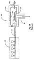
- Fig. 1B is a cross-section elevation view of station 106 of Fig. 1A, showing some additional typical features of such a processing station.
- Station 106 is based on a sealable process chamber interfacing to chamber 101 of Fig. 1A through flanged slit valve apparatus 102. It is through this interface that wafers are brought into chamber 107 for processing, and removed from chamber 107 after processing.
- Chamber 107 has a vacuum pumping port 109, through which the chamber is evacuated, and a heatable hearth 110 for supporting a wafer 111 during processing.
- Gases used in processing are introduced from a gas feed and control unit 115 through conduit(s) 114 via ring manifold 113 and showerhead manifold 112.
- chamber 101 is pumped by substantial vacuum pumps at all times to keep all of the volume in the chamber under high vacuum.
- the purpose is to avoid contamination by atmospheric gases between processing stations.
- Wafers to be processed are placed in load-lock chamber 104, typically in a carrier, and the load-lock is evacuated to a vacuum level on the order of the vacuum level in chamber 101.
- An inner valve is then opened, and wafers may then be retrieved from the load-lock by transfer apparatus 103 and transferred to any one of processing stations 1-4.
- vacuum pumping is throttled to control process chamber pressure without using excessive quantities of process gases.
- throttling may be accomplished in a number of ways, including valves having controllable openings.
- gases are valved off in unit 115 (Fig. 1B), and the throttling mechanism is opened to allow maximum pumping speed in the processing chamber.
- the purpose is to reduce the gas pressure in the processing chamber to a value close to that in transfer chamber 107.
- the slit valve in apparatus 102 is opened, and transfer apparatus 103 enters the processing chamber and retrieves the processed wafer (111).
- the retrieved wafer is typically transferred via apparatus 103 to another processing station, then a wafer from the load-lock or from another processing station is inserted and placed on hearth 111, after which the transfer apparatus withdraws.
- the slit valve associated with apparatus 102 is closed again, isolating the process chamber from transfer chamber 101. Then process gases are introduced from unit 115 through conduit(s) 114 and pumping speed is throttled.
- Fig. 2A is an isometric view of a multipurpose processing station 201 according to a preferred embodiment of the present invention, capable of performing a broad variety of processes
- Fig. 2B is an exploded view of the multipurpose processing station of Fig. 2A
- Fig. 2C is an isometric, cutaway elevation view of the multipurpose processing station shown in Figs. 2A and 2B, seen from a different perspective than that of Fig. 2A.
- Fig. 2D is an elevation section view of the multipurpose processing station of Fig. 2A, shown in processing mode
- Fig. 2E is an elevation section view of the apparatus of Fig. 2A, shown in transfer mode.
- the multipurpose station in its embodiments is a relatively complicated apparatus, several views and sections have been provided to better illustrate the features and elements of the station, and the descriptions which follow bearing on the multipurpose processing station are best understood by reference to all of the views provided.
- multipurpose processing station 201 is attached to a cluster tool by base chamber 203, which, when assembled with other elements provides vacuum integrity.
- Base chamber 203 has a side extending passage 205 ending in a flange 207 which is adapted to mount to a mating flange on a cluster tool transfer apparatus in the manner that station 104 mounts to system 100 (Fig. 1A).
- a slit valve is not shown, and in this embodiment is a part of the cluster tool apparatus to which flange 207 mounts.
- a cylindrical (in this embodiment) processing chamber 204 mounts to an upper end of base chamber 203 with vacuum seals providing vacuum integrity at the interface, and a lid assembly 261 seals to the upper end of the process chamber with vacuum seals.
- the lid assembly in this embodiment is hinged to the process chamber and also has apparatus for providing process gases into the process chamber.
- the lid assembly and associated apparatus are described more fully below. For the present portion of the description it is important to note (Figs. 2C and 2D) that the process chamber with the lid assembly and pedestal provides a closed processing volume.
- a drive assembly 209 mounts below to base chamber 203 by a horizontal flange with vacuum seals.
- the horizontal flange is a part of an upper cylindrical housing 211 which has a side outlet 213 for attachment to a vacuum pumping system not shown.
- Upper housing 211 by virtue of being rigidly mounted to base chamber 203, which is in turn rigidly mounted to the vacuum transfer chamber of a cluster tool, is a stationary element providing structural support for other elements, as will be clear from further description below.
- the purpose of the drive assembly is to raise and lower an internal pedestal apparatus 215 (Fig. 2B).
- the pedestal apparatus has a heated hearth for supporting and providing heat to a wafer to be processed.
- wafers may be inserted into the base chamber and released to lie upon the hearth, and after the transfer apparatus withdraws through extension 205 and the associated slit valve closes, the pedestal may be raised, moving the supported wafer up into a process chamber in position to be processed.
- Pedestal apparatus 215 has an upper portion 217 comprising a heater plate, an electrical insulator plate, and other elements which are described in more detail in sections below.
- the connection of the pedestal apparatus to the drive assembly is of primary interest.
- Fig. 2E shows pedestal apparatus 215 in its lowermost position having a wafer 219 supported on upper portion 217 of the pedestal apparatus.
- a transfer apparatus (103 of Fig. 1A) may enter the base chamber through extension 205 and pick and place wafers on the upper portion of the pedestal apparatus.
- wafer 219 has been placed on the pedestal apparatus.
- Pedestal apparatus 215 has an upper structure 224 and a lower extension 225 ending in a flange 227 to which an outer cylindrical member 223 is also mounted, creating an annular region therebetween.
- Outer cylindrical member 223 is lined with a bearing material and is adapted to fit closely around lower housing 221, forming thereby a vertical linear guide for raising and lowering pedestal apparatus 215 reliably with no eccentric loads.
- Vacuum integrity is maintained for the overall assembly while allowing vertical freedom of motion for the pedestal apparatus by a metal bellows 233 which seals between flange 227 at a lower end and a flange 229 affixed by its outer diameter to the lower end of lower cylindrical housing 221.
- Flange 229 is stationary, as it is a part of lower housing 221 attached to housing 211 which is mounted to base chamber 203.
- Flange 227 by virtue of being attached to lower extension 225 of pedestal apparatus 215, travels up and down with pedestal apparatus 215.
- bellows 233 extends, and as pedestal apparatus 215 is raised, bellows 233 retracts.
- the pedestal apparatus is restrained in its vertical path by the inside diameter of flange 229 and primarily by the internal bearing within cylinder 223.
- drive assembly 209 includes an electrically actuated and powered linear actuator 235 in this embodiment having an extensible shaft 237 within a guide housing 238, wherein the extensible shaft may be extended and retracted within housing 238 as initiated by control signals received from a control system not shown.
- One end of extensible shaft 237 is pivotally attached by a clevis 239 to upper housing 211 of the drive assembly.
- a yoke assembly 241 comprising a U-shaped track encircles the body of cylinder 223 (which is fixedly attached to pedestal assembly 215) and is pivotally attached at the ends of the U-shaped track to opposite ends of a clamp bar 243, and the clamp bar clamps on drive housing 238.
- yoke assembly 241 engages two bearings 245 which are mounted to opposite sides of cylinder 223.
- a clevis 249 at the center of the curved end of the U-shaped track of cam-track/yoke assembly 241, one end of an adjustable-length link 247 is pivotally fastened by a clevis 249. The opposite end of link 247 is fastened again to housing 211 by a clevis 251.
- the yoke assembly is moved as a lever having the attachment at clevis 249 as a fulcrum, such that cylinder 223 is lowered a distance about one-half the length that shaft 237 is extended, causing the entire pedestal assembly to be lowered relative to the process chamber and the base chamber.
- the pedestal assembly is similarly raised relative to the base and process chambers.
- vertical movement of the pedestal assembly which provides for a lower position for inserting and retrieving wafers through extension 205, and an upper position wherein a wafer on the pedestal is presented upward into the processing chamber for processing, also provides for a different pumping speed between the upper position and the lower. Also the elements that make this possible also allow for easy alteration of the actual pumping speed in the process position.
- a ring-shaped liner 253 is positioned at the point that base chamber 203 joins process chamber 204.
- the inside diameter of liner 253 determines area of an annular passage 255 (Fig. 2D) formed between liner 253 and the top edge of pedestal 215 when the pedestal is in the uppermost position.
- Liner 253 is also made of a material that has a relatively low coefficient of conductive heat transfer, and thereby provides protection for the parts of the process chamber and the base chamber that are closest to the heated pedestal while the pedestal is in the processing (uppermost) position.
- pedestal 215 In conjunction with liner 253, pedestal 215 is provided with an annular shroud 257 which is attached to the pedestal and forms a shaped pumping annulus.
- annulus 255 When pedestal 215 is in the uppermost position the upper annulus that shroud 257 forms with the body of pedestal 215 mates with annulus 255 by the upper rim of the shroud mating with liner 253.
- Fig. 2D it is clear that the passage for pumping from the process chamber through side outlet pumping port 213 is through the annular passage formed between shroud 257 and the body of pedestal 215.
- a lid assembly 261 comprising a lid ring 263, an insulator ring 265 and a gas diffuser assembly 267.
- Gas diffuser assembly 267 has ports not shown for introducing process gases, internal passages for conducting the process gases to the process chamber, and diffuser elements within the process region for distributing process gases evenly over a wafer on pedestal 215 in position in the process chamber to be processed. Such ports, passages and distribution elements are well-known in the art.
- Diffuser 267 is nested in an insulator ring 265 which provides electrical and thermal insulation for the diffuser assembly, and allows the diffuser assembly to be electrically biased relative to other elements as required in various process recipes. Such bias may be used to, for example, provide for exciting the process gases in the chamber to form a plasma, as known in plasma-enhanced CVD processes.
- Insulator ring 265 joins to lid ring 263 and to diffuser 267 in a manner with vacuum seals to provide vacuum integrity and to provide also a rigid lid assembly.
- lid assembly 261 is hinged to process chamber 204 with a removable vacuum seal, making access for cleaning and maintenance relatively facile and routine. In other embodiments the lid may be mounted differently and completely removed for access.
- Figs. 2D and 2E access to the inside of the process chamber may be made by releasing lid assembly 261 and moving it out of the way.
- easy access is provided to flange 227 where the lower portion 225 is fastened to flange 227.
- With the lid assembly open one may dismount pedestal assembly 215 from flange 227 and remove it from the processing station out the open top.
- FIG. 3 is a partial cross section through the top region of pedestal 215 at about the position of broken circle 269 in Fig. 2D.
- pedestal 215 is an assembly of an upper structure 224 and a lower extension 225.
- Upper structure 224 is closed at the top by a closure plate 226, and elements 225, 226, and 224 are assembled with vacuum seals providing an essentially hollow vacuum-tight structure.
- Upper closure plate 226 supports heater and electrode elements for supporting a wafer during processing as described more fully below with reference to Fig. 3.
- Closure plate 226 of pedestal assembly 215 is the base plate in Fig. 3, and is water-cooled to maintain operating temperature for vacuum seals, such as conventional o-rings and the like, and for other elements that might be damaged by high temperatures..
- closure plate 226 is penetrated in this embodiment in two places by a unique electrical feedthrough unit 301.
- a unique electrical feedthrough unit 301 is shown in Fig. 3, but in a preferred embodiment there are two such penetrations serving a unique heater plate to be described in detail below.
- Feedthrough unit 301 is adapted to closure plate 226 with vacuum seals to preserve vacuum integrity.
- Feedthrough unit 301 in one penetration of closure plate 226 provides electrical power to heating elements in a heater plate 303, which is spaced apart from closure plate 226 by in electrical insulator plate 305.
- the function of heater plate 303 is to provide heat to a susceptor 307 upon which a wafer rests during processing.
- Susceptor 307 is a mostly graphite structure which has a high coefficient of conductive heat transfer, and is spaced apart from heater plate 303 by a small distance D1. Heater plate 303 provides heat to susceptor 307 by convection and radiation across gap D1, helping to provide a relatively constant temperature across its upper surface, hence over the surface of a wafer, and also providing an efficient electrode for high frequency electrical biasing.
- the susceptor forms an electrical entity which, for those processes requiring it, is biased through an RF feedthrough, not shown in Fig. 3.
- Heater power wires connecting to two feedthroughs 301, to a second feedthrough for RF power, and miscellaneous other conduits and connectors are provided to the region of the lower surface of closure plate 226 by being guided up through the hollow interior of pedestal assembly 215 (See Figs. 2C, D, and E).
- Such wires and conduits for supplying power and other utilities to pedestal 215 subassemblies and elements are not shown in these views to promote simplicity, and extend generally from external power and utility supplies as known in the art.
- thermocouples with appropriate feedthroughs for sensing temperature of internal elements and at least one optical sensor for monitoring temperature of the susceptor.
- feedthroughs are generally known in the art.
- An air-cylinder -operated mechanism for translating a pattern of typically three ceramic pins is adapted to the heater/susceptor assembly as well, and is used to raise and lower a wafer from the surface of susceptor 307 to allow a transfer device to extend under a wafer for picking and placing wafers to and from the susceptor plate.
- a pneumatic cylinder is adapted to the underside of closure plate 226 such that the moving haft of the cylinder may be extended through an opening in the closure plate via a bellows seal.
- the pneumatic cylinder has a one-half inch stroke and operates a spider positioned below the heater that carries three ceramic pins that extend through small openings in the heater and the susceptor plate.
- a wafer on susceptor 307 may be lifted off the upper surface of the susceptor by the ceramic pins referred t above, actuated by the pneumatic cylinder described.
- a transfer arm (see Fig. 1A, item 103) may then extend into the process station beneath the a wafer on the pins but above the susceptor. Retracting the pins then places the wafer on the transfer arm, which may then be withdrawn along with the wafer. The process may be reversed for placing a new wafer to be processed on the susceptor.
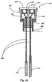
- Feedthrough 301 of Fig. 3 is shown isolated in Fig. 4A.
- a ceramic body portion 403 is joined by intermetallic bonding in this embodiment to a metal body portion 405 which has a seal grove 407 for a vacuum seal such as an o-ring, forming a unitary body sealable through an appropriate opening in closure plate 226 (Fig. 3).
- Solid nickel wires 409 are sealed through ceramic body portion 403 also by intermetallic bonding as known in the art, and are joined to conventional power wires 411 such as by soldering, at a distance great enough from the feedthrough that conducted heat will not be a problem.
- sockets 413 are constrained in the vertical direction by wires 409, which have considerable stiffness. Openings 415 are somewhat larger in diameter than the diameters of sockets 413, allowing sockets 413 lateral freedom of movement (wires 409 offer little resistance to lateral movement). This freedom of lateral movement allows for some movement and misalignment when assembling a heater plate having posts (as further described below) to a closure plate.
- Fig. 4C is a top view of feedthrough 301 of Fig. 4A
- Fig. 4B is a section view taken through the body assembly of feedthrough 301 along section line 4B-4B of Fig. 4C, which is substantially rotated ninety degrees from the section of Fig. 4A
- Section view 4B is along a groove 417 in ceramic body portion 403 below a circular declavity 419.
- Declavity 419 receives a circular portion of heater plate 303 from which connector posts extend, and groove 417 receives a baffle extension 311 of a ceramic insulator barrier 309 which serves to prevent line-of-sight electrical interaction between individual posts of the electrical feedthrough.
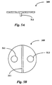
- Fig. 5A and B show a top view and a side view of ceramic insulator barrier 309, which has an overall diameter great enough to encompass the position of both sockets 413.
- Barrier 309 has circular openings 511 and 513 in this embodiment which are adapted to allow posts assembled to heater plate 303 to pass through in a manner that is described in more detail below.
- Baffle extension 311 of barrier 309 extends as a barrier wall across the diameter of barrier 309 at substantially ninety degrees to the flat body of the ceramic barrier, and is adapted to engage groove 417 when a heater plate is assembled to a pedestal in the embodiment described.
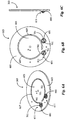
- Fig. 6A is an isometric view of heater plate 303 of Fig. 3.
- Fig. 6B is a plan view of the same heater plate, and
- Fig. 6C is a side view.
- Heater plate 303 in this embodiment is a unique two-zone heater having an inner region 603 and an outer region 605 separated by a dual channels 607 and 609 which pass through the thickness of the heater plate.
- Inner region 603 is adapted to be about the diameter of a wafer to be placed on a susceptor over the heater, and outer region 605 encompasses substantially the remainder of the area of the heater plate.
- Heater plate 303 in this embodiment is a ceramic assembly with thin-film heating elements.
- Two separate connector-post structures 611 are constructed on heater plate 303 in this embodiment, one to serve inner region 603 and the other to serve outer region 605.
- the provision of two separate regions capable of being powered independently allows tuning heat distribution to combat edge effects in heating a wafer on a susceptor overlying the two-zone heater, which allows a wafer to be heated evenly all the way to the outer diameter, a significant advance over prior art heaters.
- Figs. 7A, B, and C illustrate a unique connector post 701 used in the present embodiment in conjunction with the heater plate and socket assembly described above with reference primarily to Figs. 4A, B, and C.
- Fig. 7A is an isometric view of connector post 701
- Fig. 7B is an enlarged end view
- Fig. 7C is a section view taken along section line 7C-7C of Fig. 7B.
- Connector post 701 has a threaded portion 703, a flange 705 and a flexible-finger post extension 707.
- the overall length in the present embodiment is about one-half inch, with about one-quarter inch devoted to each of the threaded portion and the post extension, but larger and smaller posts may be used in other embodiments.
- the thread for the threaded portion is preferably a fine thread, but several different thread sizes may be used.
- connector post extension 707 of connector post 701 is divided into 12 equal flexible fingers such as fingers 709 illustrated.
- the connector post is typically made from a chemically-resistant material such as one of several types of stainless steel, and is heat treated in a manner known in the art to provide for appropriate spring tension of the fingers.
- each connector-post structure 611 has a raised land 601 with two threaded holes.
- An insulator barrier 309 is placed on each raised land, and connector posts 701 are threaded through openings 511 and 513 in the insulator barrier such that flanges 705 capture and hold the insulator barriers against the heater plate.
- Heater plate 303 is designed so that the threaded holes allow each heater post to mate with an appropriate heating element in the heater plate. It will be apparent to those with skill in the art that there are many alternative arrangements that might be made in heater design to utilize the unique structure described.
- feedthrough penetrations with feedthroughs 301 are provided in closure plate 226 in the pattern required to mate with connector-post structures 611 of a heater plate 303.
- the raised land 601 of each connector-post structure engages circular declavity 419 (see also Figs. 4A and 4B).
- baffle extension 311 of insulator baffle 309 engages groove 417, creating a no-line-of-sight connection.
- sockets 413 on wires 409 of feedthrough 301 allow some lateral movement, which, together with the flexible fingers of the posts ensures facile and positive engagement.
- drive assembly 209 described in detail above provides an efficient, smooth and extremely long-life drive for raising and lowering a pedestal assembly in various embodiments of the present invention.
- this drive There are many variations in this drive that might be used, though, and even completely different drives that might be incorporated in some embodiments while retaining a unique inventive difference over the existing art.
Landscapes
- Chemical & Material Sciences (AREA)
- Engineering & Computer Science (AREA)
- Metallurgy (AREA)
- Chemical Kinetics & Catalysis (AREA)
- Materials Engineering (AREA)
- Mechanical Engineering (AREA)
- General Chemical & Material Sciences (AREA)
- Organic Chemistry (AREA)
- Physics & Mathematics (AREA)
- Plasma & Fusion (AREA)
- Analytical Chemistry (AREA)
- Chemical Vapour Deposition (AREA)
- Container, Conveyance, Adherence, Positioning, Of Wafer (AREA)
Claims (10)
- Station de traitement pour un système d'outils en regroupement comprenant:dans laquelle, moyennant le socle de support de substrat (215) à la position de traitement, le diamètre externe du socle de support de substrat (215) et le premier diamètre interne plus grand forment un premier passage de pompage annulaire (255) qui présente une première aire annulaire déterminant une première vitesse de pompage limitée depuis la partie de chambre de traitement (204) au travers de l'orifice de pompage de vide (213) et moyennant le socle de support de substrat (215) à la position de transfert plus basse, le diamètre externe du socle de support de substrat (215) et le second diamètre interne plus grand forment un second passage de pompage annulaire (259) qui présente une seconde aire annulaire supérieure à la première aire annulaire, ce qui permet une seconde vitesse de pompage depuis la chambre de traitement (204) qui est supérieure à la première vitesse de pompage limitée.une partie de chambre de traitement (204) qui comporte une extrémité inférieure sensiblement circulaire présentant un premier diamètre interne;une partie de chambre de base (203) au-dessous de la partie de chambre de traitement (204), la partie de chambre de base (203) comportant un orifice de pompage de vide (213) et un orifice de transfert de substrat (205) et présentant un second diamètre interne, entre l'extrémité inférieure circulaire de la chambre de traitement (204) et l'orifice de pompage de vide (213), qui est supérieur au premier diamètre interne;un socle de support de substrat (215) qui comporte une surface de support supérieure sensiblement circulaire présentant un diamètre externe qui est inférieur au premier diamètre interne et qui est adapté sur la partie de chambre de base (203) au-dessous de l'orifice de transfert (205) au moyen d'une garniture d'étanchéité de vide dynamique (233) qui permet une translation verticale; etun système d'entraínement en translation verticale qui est adapté pour translater le socle de support de substrat (215) afin de placer la surface de support supérieure en une position de traitement à niveau avec l'extrémité inférieure sensiblement circulaire de la chambre de traitement (204) ou en une position de transfert plus basse dans la partie de chambre de base (203) au-dessus de l'orifice de pompage (213) et au-dessous de l'orifice de transfert (205),
- Station de traitement selon la revendication 1, dans laquelle le premier diamètre interne est formé par une bague remplaçable (253), ce qui permet que la première vitesse de pompage soit modifiée par incréments en interchangeant des bagues remplaçables présentant un diamètre externe constant et un diamètre interne variable.
- Station de traitement selon la revendication 1, comprenant en outre une enveloppe annulaire (257) qui entoure une partie du socle de substrat (215) en partant au niveau de la surface de support supérieure sensiblement circulaire et en s'étendant au-dessous de la surface de support supérieure sensiblement circulaire, où le diamètre de l'enveloppe annulaire (257) au niveau de la hauteur de la surface de support supérieure sensiblement circulaire est sensiblement égal au premier diamètre interne de telle sorte que, moyennant le socle de support de substrat (215) dans la position de traitement, l'enveloppe annulaire (257) se conjugue avec le premier diamètre interne en contraignant toute la circulation de gaz en provenance de la chambre de traitement (204) à circuler à l'intérieur de l'enveloppe annulaire (257) entre l'enveloppe annulaire et le socle de support de substrat (215).
- Station de traitement selon la revendication 1, comprenant en outre un couvercle démontable (261) qui ferme une extrémité supérieure de la chambre de traitement (204) et dans laquelle la garniture d'étanchéité de vide dynamique (233) constitue une garniture d'étanchéité démontable de telle sorte que le couvercle (261) et la garniture d'étanchéité de vide dynamique puissent être démontés, ce qui permet que le socle de support de substrat (215) soit retiré de l'intérieur de la région de chambre de base (203) vers le haut au travers de la région de chambre de traitement (204).
- Station de traitement selon la revendication 4, dans laquelle le couvercle démontable (261) comprend un système de distribution de gaz (267) pour appliquer des gaz de traitement de façon uniforme sur une surface exposée d'un substrat qui est supporté sur le socle de support de substrat (215), le socle de support de substrat étant dans la position de traitement.
- Station de traitement selon la revendication 1, dans laquelle le socle de support de substrat (215) comprend une plaque de fermeture (226) qui est parallèle à la surface de support supérieure et qui forme une frontière de vide pour la chambre de traitement (204), une plaque de moyen de chauffage (303) sur le côté de la chambre de traitement (204) isolée thermiquement de la plaque de fermeture (226) et un suscepteur isolé électriquement (307) espacé de la plaque de moyen de chauffage et au-dessus de celle-ci, le suscepteur formant la surface de support supérieure.
- Station de traitement selon la revendication 6, dans laquelle la plaque de moyen de chauffage (303) est une plaque de moyen de chauffage sensiblement circulaire qui comporte des régions de chauffage interne et externe alimentées séparément (603, 605), ce qui permet qu'un profil de température sur la plaque soit géré en gérant la puissance sur les régions de chauffage interne et externe alimentées séparément (603, 605).
- Station de traitement selon la revendication 7, dans laquelle la région de chauffage interne est séparée de la région de chauffage externe par au moins une gorge en arc circulaire (607, 609) au travers de la plaque de moyen de chauffage (303).
- Station de traitement selon la revendication 7, dans laquelle la région de chauffage interne (603) présente un diamètre qui est sensiblement égal au diamètre d'un substrat qui est destiné à être chauffé par la plaque de moyen de chauffage (303).
- Station de traitement selon la revendication 1, dans laquelle la garniture d'étanchéité de vide dynamique est constituée par un soufflet en acier inoxydable (233).
Applications Claiming Priority (3)
| Application Number | Priority Date | Filing Date | Title |
|---|---|---|---|
| US08/810,255 US5855675A (en) | 1997-03-03 | 1997-03-03 | Multipurpose processing chamber for chemical vapor deposition processes |
| US810255 | 1997-03-03 | ||
| PCT/US1998/004062 WO1998039495A1 (fr) | 1997-03-03 | 1998-03-02 | Chambre de traitement polyvalente pour depots chimiques en phase vapeur |
Publications (3)
| Publication Number | Publication Date |
|---|---|
| EP0972092A1 EP0972092A1 (fr) | 2000-01-19 |
| EP0972092A4 EP0972092A4 (fr) | 2002-04-10 |
| EP0972092B1 true EP0972092B1 (fr) | 2005-05-25 |
Family
ID=25203405
Family Applications (1)
| Application Number | Title | Priority Date | Filing Date |
|---|---|---|---|
| EP98908858A Expired - Lifetime EP0972092B1 (fr) | 1997-03-03 | 1998-03-02 | Chambre de traitement polyvalente pour depots chimiques en phase vapeur |
Country Status (5)
| Country | Link |
|---|---|
| US (1) | US5855675A (fr) |
| EP (1) | EP0972092B1 (fr) |
| JP (1) | JP3217798B2 (fr) |
| DE (1) | DE69830310T2 (fr) |
| WO (1) | WO1998039495A1 (fr) |
Cited By (1)
| Publication number | Priority date | Publication date | Assignee | Title |
|---|---|---|---|---|
| US10177050B2 (en) * | 2012-04-26 | 2019-01-08 | Applied Materials, Inc. | Methods and apparatus for controlling substrate uniformity |
Families Citing this family (109)
| Publication number | Priority date | Publication date | Assignee | Title |
|---|---|---|---|---|
| US6174377B1 (en) * | 1997-03-03 | 2001-01-16 | Genus, Inc. | Processing chamber for atomic layer deposition processes |
| US6482747B1 (en) * | 1997-12-26 | 2002-11-19 | Hitachi, Ltd. | Plasma treatment method and plasma treatment apparatus |
| US6190732B1 (en) | 1998-09-03 | 2001-02-20 | Cvc Products, Inc. | Method and system for dispensing process gas for fabricating a device on a substrate |
| US6364954B2 (en) * | 1998-12-14 | 2002-04-02 | Applied Materials, Inc. | High temperature chemical vapor deposition chamber |
| JP2000323487A (ja) * | 1999-05-14 | 2000-11-24 | Tokyo Electron Ltd | 枚葉式熱処理装置 |
| US6144013A (en) * | 1999-07-01 | 2000-11-07 | International Business Machines Corporation | Local humidity control system for low temperature electronic module |
| FI110311B (fi) * | 1999-07-20 | 2002-12-31 | Asm Microchemistry Oy | Menetelmä ja laitteisto aineiden poistamiseksi kaasuista |
| US6178660B1 (en) * | 1999-08-03 | 2001-01-30 | International Business Machines Corporation | Pass-through semiconductor wafer processing tool and process for gas treating a moving semiconductor wafer |
| US6472643B1 (en) * | 2000-03-07 | 2002-10-29 | Silicon Valley Group, Inc. | Substrate thermal management system |
| US6414276B1 (en) | 2000-03-07 | 2002-07-02 | Silicon Valley Group, Inc. | Method for substrate thermal management |
| US7060132B2 (en) * | 2000-04-14 | 2006-06-13 | Asm International N.V. | Method and apparatus of growing a thin film |
| TW496907B (en) * | 2000-04-14 | 2002-08-01 | Asm Microchemistry Oy | Method and apparatus of growing a thin film onto a substrate |
| JP2002035572A (ja) * | 2000-05-18 | 2002-02-05 | Ulvac Japan Ltd | 真空処理装置と多室型真空処理装置 |
| ATE280436T1 (de) * | 2000-06-22 | 2004-11-15 | Unaxis Balzers Ag | Beschichtungsanlage für scheibenförmige werkstücke |
| US6620723B1 (en) * | 2000-06-27 | 2003-09-16 | Applied Materials, Inc. | Formation of boride barrier layers using chemisorption techniques |
| US7732327B2 (en) | 2000-06-28 | 2010-06-08 | Applied Materials, Inc. | Vapor deposition of tungsten materials |
| US7964505B2 (en) * | 2005-01-19 | 2011-06-21 | Applied Materials, Inc. | Atomic layer deposition of tungsten materials |
| US6551929B1 (en) * | 2000-06-28 | 2003-04-22 | Applied Materials, Inc. | Bifurcated deposition process for depositing refractory metal layers employing atomic layer deposition and chemical vapor deposition techniques |
| US7101795B1 (en) | 2000-06-28 | 2006-09-05 | Applied Materials, Inc. | Method and apparatus for depositing refractory metal layers employing sequential deposition techniques to form a nucleation layer |
| US7405158B2 (en) | 2000-06-28 | 2008-07-29 | Applied Materials, Inc. | Methods for depositing tungsten layers employing atomic layer deposition techniques |
| US6235656B1 (en) | 2000-07-03 | 2001-05-22 | Andrew Peter Clarke | Dual degas/cool loadlock cluster tool |
| US6562141B2 (en) | 2000-07-03 | 2003-05-13 | Andrew Peter Clarke | Dual degas/cool loadlock cluster tool |
| US6692324B2 (en) * | 2000-08-29 | 2004-02-17 | Ut-Battelle, Llc | Single self-aligned carbon containing tips |
| US6428847B1 (en) * | 2000-10-16 | 2002-08-06 | Primaxx, Inc. | Vortex based CVD reactor |
| WO2002045871A1 (fr) * | 2000-12-06 | 2002-06-13 | Angstron Systems, Inc. | Systeme et procede de depot module d'une couche atomique induite par des ions |
| US7270724B2 (en) | 2000-12-13 | 2007-09-18 | Uvtech Systems, Inc. | Scanning plasma reactor |
| US6630201B2 (en) | 2001-04-05 | 2003-10-07 | Angstron Systems, Inc. | Adsorption process for atomic layer deposition |
| US6800173B2 (en) | 2000-12-15 | 2004-10-05 | Novellus Systems, Inc. | Variable gas conductance control for a process chamber |
| US20020083897A1 (en) * | 2000-12-29 | 2002-07-04 | Applied Materials, Inc. | Full glass substrate deposition in plasma enhanced chemical vapor deposition |
| US6825447B2 (en) * | 2000-12-29 | 2004-11-30 | Applied Materials, Inc. | Apparatus and method for uniform substrate heating and contaminate collection |
| US6998579B2 (en) | 2000-12-29 | 2006-02-14 | Applied Materials, Inc. | Chamber for uniform substrate heating |
| US6765178B2 (en) | 2000-12-29 | 2004-07-20 | Applied Materials, Inc. | Chamber for uniform substrate heating |
| US6773683B2 (en) * | 2001-01-08 | 2004-08-10 | Uvtech Systems, Inc. | Photocatalytic reactor system for treating flue effluents |
| US6951804B2 (en) | 2001-02-02 | 2005-10-04 | Applied Materials, Inc. | Formation of a tantalum-nitride layer |
| US6547876B2 (en) | 2001-02-07 | 2003-04-15 | Emcore Corporation | Apparatus for growing epitaxial layers on wafers by chemical vapor deposition |
| US6878206B2 (en) | 2001-07-16 | 2005-04-12 | Applied Materials, Inc. | Lid assembly for a processing system to facilitate sequential deposition techniques |
| US6660126B2 (en) | 2001-03-02 | 2003-12-09 | Applied Materials, Inc. | Lid assembly for a processing system to facilitate sequential deposition techniques |
| US6734020B2 (en) | 2001-03-07 | 2004-05-11 | Applied Materials, Inc. | Valve control system for atomic layer deposition chamber |
| US20020144786A1 (en) * | 2001-04-05 | 2002-10-10 | Angstron Systems, Inc. | Substrate temperature control in an ALD reactor |
| JP2002343786A (ja) * | 2001-05-21 | 2002-11-29 | Tokyo Electron Ltd | 半導体処理装置 |
| US20070009658A1 (en) * | 2001-07-13 | 2007-01-11 | Yoo Jong H | Pulse nucleation enhanced nucleation technique for improved step coverage and better gap fill for WCVD process |
| US7211144B2 (en) * | 2001-07-13 | 2007-05-01 | Applied Materials, Inc. | Pulsed nucleation deposition of tungsten layers |
| US7085616B2 (en) | 2001-07-27 | 2006-08-01 | Applied Materials, Inc. | Atomic layer deposition apparatus |
| US7049226B2 (en) * | 2001-09-26 | 2006-05-23 | Applied Materials, Inc. | Integration of ALD tantalum nitride for copper metallization |
| US20030059538A1 (en) * | 2001-09-26 | 2003-03-27 | Applied Materials, Inc. | Integration of barrier layer and seed layer |
| US6936906B2 (en) | 2001-09-26 | 2005-08-30 | Applied Materials, Inc. | Integration of barrier layer and seed layer |
| US6916398B2 (en) * | 2001-10-26 | 2005-07-12 | Applied Materials, Inc. | Gas delivery apparatus and method for atomic layer deposition |
| KR100443121B1 (ko) * | 2001-11-29 | 2004-08-04 | 삼성전자주식회사 | 반도체 공정의 수행 방법 및 반도체 공정 장치 |
| US6729824B2 (en) | 2001-12-14 | 2004-05-04 | Applied Materials, Inc. | Dual robot processing system |
| US6620670B2 (en) | 2002-01-18 | 2003-09-16 | Applied Materials, Inc. | Process conditions and precursors for atomic layer deposition (ALD) of AL2O3 |
| US6911391B2 (en) * | 2002-01-26 | 2005-06-28 | Applied Materials, Inc. | Integration of titanium and titanium nitride layers |
| US6998014B2 (en) | 2002-01-26 | 2006-02-14 | Applied Materials, Inc. | Apparatus and method for plasma assisted deposition |
| US6827978B2 (en) * | 2002-02-11 | 2004-12-07 | Applied Materials, Inc. | Deposition of tungsten films |
| US6833161B2 (en) * | 2002-02-26 | 2004-12-21 | Applied Materials, Inc. | Cyclical deposition of tungsten nitride for metal oxide gate electrode |
| US7439191B2 (en) * | 2002-04-05 | 2008-10-21 | Applied Materials, Inc. | Deposition of silicon layers for active matrix liquid crystal display (AMLCD) applications |
| US6720027B2 (en) | 2002-04-08 | 2004-04-13 | Applied Materials, Inc. | Cyclical deposition of a variable content titanium silicon nitride layer |
| US6846516B2 (en) * | 2002-04-08 | 2005-01-25 | Applied Materials, Inc. | Multiple precursor cyclical deposition system |
| US20030194825A1 (en) * | 2002-04-10 | 2003-10-16 | Kam Law | Deposition of gate metallization for active matrix liquid crystal display (AMLCD) applications |
| US6875271B2 (en) | 2002-04-09 | 2005-04-05 | Applied Materials, Inc. | Simultaneous cyclical deposition in different processing regions |
| US6869838B2 (en) * | 2002-04-09 | 2005-03-22 | Applied Materials, Inc. | Deposition of passivation layers for active matrix liquid crystal display (AMLCD) applications |
| US7279432B2 (en) | 2002-04-16 | 2007-10-09 | Applied Materials, Inc. | System and method for forming an integrated barrier layer |
| US20040036129A1 (en) * | 2002-08-22 | 2004-02-26 | Micron Technology, Inc. | Atomic layer deposition of CMOS gates with variable work functions |
| US6967154B2 (en) * | 2002-08-26 | 2005-11-22 | Micron Technology, Inc. | Enhanced atomic layer deposition |
| US20040065255A1 (en) * | 2002-10-02 | 2004-04-08 | Applied Materials, Inc. | Cyclical layer deposition system |
| US6821563B2 (en) | 2002-10-02 | 2004-11-23 | Applied Materials, Inc. | Gas distribution system for cyclical layer deposition |
| US6916374B2 (en) * | 2002-10-08 | 2005-07-12 | Micron Technology, Inc. | Atomic layer deposition methods and atomic layer deposition tools |
| US7427426B2 (en) * | 2002-11-06 | 2008-09-23 | Tokyo Electron Limited | CVD method for forming metal film by using metal carbonyl gas |
| US7262133B2 (en) | 2003-01-07 | 2007-08-28 | Applied Materials, Inc. | Enhancement of copper line reliability using thin ALD tan film to cap the copper line |
| US20040134427A1 (en) * | 2003-01-09 | 2004-07-15 | Derderian Garo J. | Deposition chamber surface enhancement and resulting deposition chambers |
| US7981473B2 (en) * | 2003-04-23 | 2011-07-19 | Aixtron, Inc. | Transient enhanced atomic layer deposition |
| US7211508B2 (en) | 2003-06-18 | 2007-05-01 | Applied Materials, Inc. | Atomic layer deposition of tantalum based barrier materials |
| US6899545B2 (en) * | 2003-10-16 | 2005-05-31 | Special Hermetic Products, Inc. | Coupling and method for producing a hermetic seal |
| US8202575B2 (en) * | 2004-06-28 | 2012-06-19 | Cambridge Nanotech, Inc. | Vapor deposition systems and methods |
| JP4820137B2 (ja) * | 2005-09-26 | 2011-11-24 | 株式会社日立国際電気 | 発熱体の保持構造体 |
| EP1957688A2 (fr) | 2005-11-22 | 2008-08-20 | Genus, Inc. | Appareil de depot de couche atomique (ald) a tranche unique et a ecoulement symetrique de petit volume |
| DE102005056323A1 (de) * | 2005-11-25 | 2007-05-31 | Aixtron Ag | Prozesskammermodul zum gleichzeitigen Abscheiden von Schichten auf mehreren Substraten |
| US20070240631A1 (en) * | 2006-04-14 | 2007-10-18 | Applied Materials, Inc. | Epitaxial growth of compound nitride semiconductor structures |
| US20070256635A1 (en) * | 2006-05-02 | 2007-11-08 | Applied Materials, Inc. A Delaware Corporation | UV activation of NH3 for III-N deposition |
| US8821637B2 (en) * | 2007-01-29 | 2014-09-02 | Applied Materials, Inc. | Temperature controlled lid assembly for tungsten nitride deposition |
| US20080314311A1 (en) * | 2007-06-24 | 2008-12-25 | Burrows Brian H | Hvpe showerhead design |
| US20090149008A1 (en) * | 2007-10-05 | 2009-06-11 | Applied Materials, Inc. | Method for depositing group iii/v compounds |
| US20100111650A1 (en) * | 2008-01-31 | 2010-05-06 | Applied Materials, Inc. | Automatic substrate loading station |
| US20090194026A1 (en) * | 2008-01-31 | 2009-08-06 | Burrows Brian H | Processing system for fabricating compound nitride semiconductor devices |
| US20110070370A1 (en) | 2008-05-28 | 2011-03-24 | Aixtron Ag | Thermal gradient enhanced chemical vapour deposition (tge-cvd) |
| JP2011525719A (ja) * | 2008-06-24 | 2011-09-22 | アプライド マテリアルズ インコーポレイテッド | 低温pecvd用途用のペデスタルヒータ |
| US8440048B2 (en) | 2009-01-28 | 2013-05-14 | Asm America, Inc. | Load lock having secondary isolation chamber |
| US8491720B2 (en) * | 2009-04-10 | 2013-07-23 | Applied Materials, Inc. | HVPE precursor source hardware |
| US8183132B2 (en) | 2009-04-10 | 2012-05-22 | Applied Materials, Inc. | Methods for fabricating group III nitride structures with a cluster tool |
| JP2012525013A (ja) * | 2009-04-24 | 2012-10-18 | アプライド マテリアルズ インコーポレイテッド | 後続の高温でのiii族堆積用の基板前処理 |
| US20100273291A1 (en) * | 2009-04-28 | 2010-10-28 | Applied Materials, Inc. | Decontamination of mocvd chamber using nh3 purge after in-situ cleaning |
| JP2012525718A (ja) * | 2009-04-29 | 2012-10-22 | アプライド マテリアルズ インコーポレイテッド | HVPEにおいてその場プレ−GaN堆積層を形成する方法 |
| US20110256692A1 (en) | 2010-04-14 | 2011-10-20 | Applied Materials, Inc. | Multiple precursor concentric delivery showerhead |
| US9443753B2 (en) * | 2010-07-30 | 2016-09-13 | Applied Materials, Inc. | Apparatus for controlling the flow of a gas in a process chamber |
| US9076827B2 (en) | 2010-09-14 | 2015-07-07 | Applied Materials, Inc. | Transfer chamber metrology for improved device yield |
| TWI534291B (zh) | 2011-03-18 | 2016-05-21 | 應用材料股份有限公司 | 噴淋頭組件 |
| WO2012134605A1 (fr) * | 2011-03-25 | 2012-10-04 | Applied Materials, Inc. | Procédé et appareil pour installation ou remplacement de thermocouple dans un support de substrat |
| JP5426618B2 (ja) * | 2011-07-19 | 2014-02-26 | 株式会社日立国際電気 | 絶縁構造体、加熱装置、基板処理装置および半導体装置の製造方法 |
| DE102012103295A1 (de) | 2012-01-09 | 2013-07-11 | Aixtron Se | Räumlich optimierte Anordnung zum Bearbeiten von Halbleitersubstraten |
| US9879684B2 (en) * | 2012-09-13 | 2018-01-30 | Kla-Tencor Corporation | Apparatus and method for shielding a controlled pressure environment |
| DE102013111790A1 (de) | 2013-10-25 | 2015-04-30 | Aixtron Se | Energie- und materialverbrauchsoptimierter CVD-Reaktor |
| DE102013113052A1 (de) | 2013-11-26 | 2015-05-28 | Aixtron Se | Heizeinrichtung für einen CVD-Reaktor |
| US9435031B2 (en) | 2014-01-07 | 2016-09-06 | International Business Machines Corporation | Microwave plasma and ultraviolet assisted deposition apparatus and method for material deposition using the same |
| CN105431924B (zh) * | 2014-04-09 | 2020-11-17 | 应用材料公司 | 用于解决具有改良的流动均匀性/气体传导性的可变的处理容积的对称腔室主体设计架构 |
| US10186450B2 (en) * | 2014-07-21 | 2019-01-22 | Asm Ip Holding B.V. | Apparatus and method for adjusting a pedestal assembly for a reactor |
| US10883168B2 (en) | 2014-09-11 | 2021-01-05 | Massachusetts Institute Of Technology | Processing system for small substrates |
| US10704142B2 (en) * | 2017-07-27 | 2020-07-07 | Applied Materials, Inc. | Quick disconnect resistance temperature detector assembly for rotating pedestal |
| US11270898B2 (en) | 2018-09-16 | 2022-03-08 | Applied Materials, Inc. | Apparatus for enhancing flow uniformity in a process chamber |
| JP2020147772A (ja) * | 2019-03-11 | 2020-09-17 | 東京エレクトロン株式会社 | 成膜装置及び成膜方法 |
| DE102020103947A1 (de) * | 2020-02-14 | 2021-08-19 | AIXTRON Ltd. | CVD-Reaktor und Verfahren zum Handhaben einer Prozesskammer-Deckenplatte |
Family Cites Families (7)
| Publication number | Priority date | Publication date | Assignee | Title |
|---|---|---|---|---|
| US5156820A (en) * | 1989-05-15 | 1992-10-20 | Rapro Technology, Inc. | Reaction chamber with controlled radiant energy heating and distributed reactant flow |
| US5078851A (en) * | 1989-07-26 | 1992-01-07 | Kouji Nishihata | Low-temperature plasma processor |
| US5294778A (en) * | 1991-09-11 | 1994-03-15 | Lam Research Corporation | CVD platen heater system utilizing concentric electric heating elements |
| JP2662365B2 (ja) * | 1993-01-28 | 1997-10-08 | アプライド マテリアルズ インコーポレイテッド | 改良された排出システムを有する単一基板式の真空処理装置 |
| JPH06275528A (ja) * | 1993-03-18 | 1994-09-30 | Hitachi Ltd | 真空処理装置の排気部構造 |
| US5772770A (en) * | 1995-01-27 | 1998-06-30 | Kokusai Electric Co, Ltd. | Substrate processing apparatus |
| JPH08260158A (ja) * | 1995-01-27 | 1996-10-08 | Kokusai Electric Co Ltd | 基板処理装置 |
-
1997
- 1997-03-03 US US08/810,255 patent/US5855675A/en not_active Expired - Lifetime
-
1998
- 1998-03-02 DE DE69830310T patent/DE69830310T2/de not_active Expired - Lifetime
- 1998-03-02 JP JP53866898A patent/JP3217798B2/ja not_active Expired - Lifetime
- 1998-03-02 WO PCT/US1998/004062 patent/WO1998039495A1/fr not_active Ceased
- 1998-03-02 EP EP98908858A patent/EP0972092B1/fr not_active Expired - Lifetime
Cited By (1)
| Publication number | Priority date | Publication date | Assignee | Title |
|---|---|---|---|---|
| US10177050B2 (en) * | 2012-04-26 | 2019-01-08 | Applied Materials, Inc. | Methods and apparatus for controlling substrate uniformity |
Also Published As
| Publication number | Publication date |
|---|---|
| WO1998039495A1 (fr) | 1998-09-11 |
| US5855675A (en) | 1999-01-05 |
| JP2000510652A (ja) | 2000-08-15 |
| JP3217798B2 (ja) | 2001-10-15 |
| DE69830310T2 (de) | 2006-01-26 |
| DE69830310D1 (de) | 2005-06-30 |
| EP0972092A4 (fr) | 2002-04-10 |
| EP0972092A1 (fr) | 2000-01-19 |
Similar Documents
| Publication | Publication Date | Title |
|---|---|---|
| EP0972092B1 (fr) | Chambre de traitement polyvalente pour depots chimiques en phase vapeur | |
| EP1159465B1 (fr) | Procedes de depot en couches atomiques | |
| TWI804537B (zh) | 低溫冷卻的可旋轉靜電卡盤 | |
| US9074284B2 (en) | Heat treatment apparatus | |
| US7682454B2 (en) | Perimeter partition-valve with protected seals and associated small size process chambers and multiple chamber systems | |
| US9484233B2 (en) | Carousel reactor for multi-station, sequential processing systems | |
| US5336324A (en) | Apparatus for depositing a coating on a substrate | |
| US9252037B2 (en) | Vacuum treatment apparatus and a method for manufacturing | |
| JP3178824B2 (ja) | 複合形単一ウエーハ用の高生産性形マルチステーシヨン方式処理装置 | |
| US20120009765A1 (en) | Compartmentalized chamber | |
| US6371712B1 (en) | Support frame for substrates | |
| US20030019428A1 (en) | Chemical vapor deposition chamber | |
| KR20000069146A (ko) | 화학 기상 증착 장치 | |
| US20260058096A1 (en) | Process module chamber providing symmetric rf return path | |
| US20150368830A1 (en) | One-piece injector assembly and one-piece exhaust liner | |
| TW202232648A (zh) | 用於提供對稱射頻返回路徑的預裝載碗機構 | |
| KR20230087601A (ko) | 더 높은 처리량 및 더 빠른 전이 시간을 위한 반도체 프로세싱 챔버 아키텍처 | |
| US11946140B2 (en) | Hot showerhead | |
| US12557254B2 (en) | Two-piece RF shield design | |
| KR20230084307A (ko) | 대칭 라디오 주파수 귀환 경로를 제공하기 위한 동적 인터페이스 | |
| KR20120077887A (ko) | 기판 처리 장치 |
Legal Events
| Date | Code | Title | Description |
|---|---|---|---|
| PUAI | Public reference made under article 153(3) epc to a published international application that has entered the european phase |
Free format text: ORIGINAL CODE: 0009012 |
|
| 17P | Request for examination filed |
Effective date: 19990915 |
|
| AK | Designated contracting states |
Kind code of ref document: A1 Designated state(s): DE FR GB IT NL |
|
| RIC1 | Information provided on ipc code assigned before grant |
Free format text: 7C 23C 16/00 A, 7C 23C 16/44 B |
|
| A4 | Supplementary search report drawn up and despatched |
Effective date: 20020225 |
|
| AK | Designated contracting states |
Kind code of ref document: A4 Designated state(s): DE FR GB IT NL |
|
| 17Q | First examination report despatched |
Effective date: 20031219 |
|
| GRAP | Despatch of communication of intention to grant a patent |
Free format text: ORIGINAL CODE: EPIDOSNIGR1 |
|
| GRAP | Despatch of communication of intention to grant a patent |
Free format text: ORIGINAL CODE: EPIDOSNIGR1 |
|
| GRAS | Grant fee paid |
Free format text: ORIGINAL CODE: EPIDOSNIGR3 |
|
| GRAA | (expected) grant |
Free format text: ORIGINAL CODE: 0009210 |
|
| AK | Designated contracting states |
Kind code of ref document: B1 Designated state(s): DE FR GB IT NL |
|
| PG25 | Lapsed in a contracting state [announced via postgrant information from national office to epo] |
Ref country code: NL Free format text: LAPSE BECAUSE OF FAILURE TO SUBMIT A TRANSLATION OF THE DESCRIPTION OR TO PAY THE FEE WITHIN THE PRESCRIBED TIME-LIMIT Effective date: 20050525 Ref country code: IT Free format text: LAPSE BECAUSE OF FAILURE TO SUBMIT A TRANSLATION OF THE DESCRIPTION OR TO PAY THE FEE WITHIN THE PRESCRIBED TIME-LIMIT;WARNING: LAPSES OF ITALIAN PATENTS WITH EFFECTIVE DATE BEFORE 2007 MAY HAVE OCCURRED AT ANY TIME BEFORE 2007. THE CORRECT EFFECTIVE DATE MAY BE DIFFERENT FROM THE ONE RECORDED. Effective date: 20050525 |
|
| REG | Reference to a national code |
Ref country code: GB Ref legal event code: FG4D |
|
| REF | Corresponds to: |
Ref document number: 69830310 Country of ref document: DE Date of ref document: 20050630 Kind code of ref document: P |
|
| NLV1 | Nl: lapsed or annulled due to failure to fulfill the requirements of art. 29p and 29m of the patents act | ||
| PLBE | No opposition filed within time limit |
Free format text: ORIGINAL CODE: 0009261 |
|
| STAA | Information on the status of an ep patent application or granted ep patent |
Free format text: STATUS: NO OPPOSITION FILED WITHIN TIME LIMIT |
|
| ET | Fr: translation filed | ||
| 26N | No opposition filed |
Effective date: 20060228 |
|
| PGFP | Annual fee paid to national office [announced via postgrant information from national office to epo] |
Ref country code: GB Payment date: 20070307 Year of fee payment: 10 |
|
| GBPC | Gb: european patent ceased through non-payment of renewal fee |
Effective date: 20080302 |
|
| PG25 | Lapsed in a contracting state [announced via postgrant information from national office to epo] |
Ref country code: GB Free format text: LAPSE BECAUSE OF NON-PAYMENT OF DUE FEES Effective date: 20080302 |
|
| PGFP | Annual fee paid to national office [announced via postgrant information from national office to epo] |
Ref country code: FR Payment date: 20120406 Year of fee payment: 15 |
|
| PGFP | Annual fee paid to national office [announced via postgrant information from national office to epo] |
Ref country code: DE Payment date: 20130410 Year of fee payment: 16 |
|
| REG | Reference to a national code |
Ref country code: FR Ref legal event code: ST Effective date: 20131129 |
|
| PG25 | Lapsed in a contracting state [announced via postgrant information from national office to epo] |
Ref country code: FR Free format text: LAPSE BECAUSE OF NON-PAYMENT OF DUE FEES Effective date: 20130402 |
|
| REG | Reference to a national code |
Ref country code: DE Ref legal event code: R119 Ref document number: 69830310 Country of ref document: DE |
|
| REG | Reference to a national code |
Ref country code: DE Ref legal event code: R119 Ref document number: 69830310 Country of ref document: DE Effective date: 20141001 |
|
| PG25 | Lapsed in a contracting state [announced via postgrant information from national office to epo] |
Ref country code: DE Free format text: LAPSE BECAUSE OF NON-PAYMENT OF DUE FEES Effective date: 20141001 |