EP0973074A1 - Dispositif de formation d'images et procede de formation d'images utilisant l'electrophotographie - Google Patents
Dispositif de formation d'images et procede de formation d'images utilisant l'electrophotographie Download PDFInfo
- Publication number
- EP0973074A1 EP0973074A1 EP98911015A EP98911015A EP0973074A1 EP 0973074 A1 EP0973074 A1 EP 0973074A1 EP 98911015 A EP98911015 A EP 98911015A EP 98911015 A EP98911015 A EP 98911015A EP 0973074 A1 EP0973074 A1 EP 0973074A1
- Authority
- EP
- European Patent Office
- Prior art keywords
- photosensitive member
- image
- electric field
- charge erasing
- alternating current
- Prior art date
- Legal status (The legal status is an assumption and is not a legal conclusion. Google has not performed a legal analysis and makes no representation as to the accuracy of the status listed.)
- Withdrawn
Links
Images


Classifications
-
- G—PHYSICS
- G03—PHOTOGRAPHY; CINEMATOGRAPHY; ANALOGOUS TECHNIQUES USING WAVES OTHER THAN OPTICAL WAVES; ELECTROGRAPHY; HOLOGRAPHY
- G03G—ELECTROGRAPHY; ELECTROPHOTOGRAPHY; MAGNETOGRAPHY
- G03G21/00—Arrangements not provided for by groups G03G13/00 - G03G19/00, e.g. cleaning, elimination of residual charge
- G03G21/06—Eliminating residual charges from a reusable imaging member
Definitions
- the present invention relates to an electrophotographic image-forming apparatus and an electrophotographic image-forming method utilizing an electrophotographic photosensitive member of high gamma, in particular, an electrophotographic photosensitive member for digital photo-input. More precisely, the present invention relates to an electrophotographic image-forming apparatus and an electrophotographic image-forming method utilizing a novel charge erasing method.
- conventional electrophotographic image-forming apparatuses have, for example, a structure comprising, around a rotatably maintained cylindrical photosensitive member 1, a main electrifier 2, light exposure means 3, image development means 4, image transfer means 5, cleaning means 6, and charge erasing (eliminating) light source 7 in this order, and charge erasing of the photosensitive member is attained by light-exposing the surface of the photosensitive member 1 by means of the charge erasing light source 7.
- Japanese Patent Publication (Kokoku) No. 5-19140 discloses an electrophotographic photosensitive member for digital photo-input having a gamma for latent image of 6 or more, which comprises a photosensitive layer consisting of intrinsic semiconductor fine powder contained in a binder having a high volume resistivity.
- Japanese Patent Unexamined Publication (Kokai) No. 8-286396 also discloses a photosensitive member having a gamma value of 2 to less than 6.
- sensitivity shift i.e., shift of the sensitivity curve of the photosensitive member in the higher sensitivity direction due to the residual charge in the photosensitive member caused by repetition of image formation.
- a larger light exposure amount for charge erasing may excite a deeper portion of the photosensitive member by its photocurrent, thereby providing uniform charge distribution.
- the light energy may accelerate yield of the binder of the photosensitive member, and hence dark decay may become faster. This may make sequential image-forming operations impossible.
- Japanese Patent Unexamined Publication (Kokai) No. 4-337762 proposes a method comprising controlling light exposure amounts for image formation and charge erasing to be in a particular relationship in order to solve the aforementioned problem of hysteresis.
- This method may achieve the desired effect for a photosensitive member of a gamma for latent image of less than 3.
- the gamma for latent image is 3 or higher, completely stable operation cannot be performed even with this technique, because of sensitivity variation due to ununiform electrification after repeated image formation and the like.
- the object of the present invention is to provide an image-forming apparatus and an image-forming method that can solve the aforementioned problems, specifically an apparatus and a method enabling effective uniform charge erasing (eliminating), hence not causing the so-called hysteresis or sensitivity shift even in continuous image formation, and capable of stably forming images of high quality and high resolution without residual images in electrophotographic image formation utilizing a high-gamma photosensitive member.
- the image-forming apparatus of the present invention comprises a photosensitive member having a gamma for latent image of 3 or more, electrification means, light exposure means, image development means, image transfer means, cleaning means, and a charge erasing (eliminating) light source, wherein the image-forming apparatus further comprises electric field applying means for applying an alternating current electric field at a frequency of 50 Hz to 1 kHz to a portion of the photosensitive member which is excited through light exposure by the charge erasing light source.
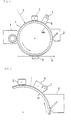
- One embodiment of the image-forming apparatus of the present invention is an image-forming apparatus comprising, around a rotatably maintained cylindrical photosensitive member 1 having a gamma for latent image of 3 or more, a main electrifier 2, a light exposure means 3, an image development means 4, an image transfer means 5, and a cleaning means 6 in this order, wherein the image-forming apparatus comprises a charge erasing light source 7 for light exposure of photosensitive member surface and the electric field applying means 9 for applying an alternating current electric field at a frequency of 50 Hz to 1 kHz to a portion of the photosensitive member which is excited through light exposure by the charge erasing light source between the cleaning means 6 and the main electrifier 2 (Fig. 1).
- an alternating current electrifier which is the electric field applying means 9 may be provided between the charge erasing light source 7 and the photosensitive member surface which is light-exposed by the charge erasing light source, and applies an alternating current electric field at a frequency of 50 Hz to 1 kHz to a portion of the photosensitive member excited through light exposure by the charge erasing light source (Fig. 1).
- an alternating current electrifier which is the electric field applying means 9 may be provided immediately after the charge erasing light source 7 with respect to the photosensitive member surface, and applies an alternating current electric field at a frequency of 50 Hz to 1 kHz to a portion of the photosensitive member which is excited through light exposure by the charge erasing light source (Fig. 2).
- the electric field applying means may be a contact electrifier 9a generating an alternating current electric field at a frequency of 50 Hz to 1 kHz, which is provided immediately after the charge erasing light source 7a with respect to the photosensitive member surface so that a portion of the photosensitive member which is excited through light exposure by the charge erasing light source 7a is contacted by the contact electrifier 9a, and applied with an alternating current electric field at a frequency of 50 Hz to 1 kHz (Fig. 3).
- the charge erasing light source 7 is provided with a filter which cuts light of a wavelength shorter than sensitization wavelength for the photosensitive member by 150 nm or more (Fig. 4).
- a direct current electric field is superimposed on the alternating current field generated by the alternating current electrifier, which is the electric field applying means, by using a direct current bias voltage from a power source 11 ranging from -1 kV to +1 kV, so that both of the fields are applied to the surface portion of the photosensitive member excited through the light exposure (Fig. 4).
- the present invention also provides a method for electrophotographic image formation comprising electrification of a photosensitive member having a gamma for latent image of 3 or more, light exposure of the member, image development, image transfer, and charge erasing of the photosensitive member, wherein the charge erasing of the photosensitive member is performed by light-exposing a surface portion of the photosensitive member with a charge erasing light source, and applying an alternating current electric field at a frequency of 50 Hz to 1 kHz to the portion of the photosensitive member while the portion is excited by the light exposure.
- the image-forming apparatus and the image-forming method of the present invention are characterized by, in such electrophotographic image-forming apparatus and method as mentioned above, applying an alternating current electric field to a photosensitive member in a state excited through light exposure by charge erasing light for charge erasing of the photosensitive member before the main electrification.
- the charge erasing light generates movable charge in the photosensitive member (the term "photosensitive member excited through light exposure" herein used means the member that is in such a state where freely movable charge is generated as mentioned above).
- the generated charge is alternately moved by the alternating current electric field in the photosensitive member, and thus localized residual charge is eliminated or uniformized to a certain level.
- High-gamma photosensitive members such as those having a gamma for latent image of 6 or more disclosed in, for example, Japanese Patent Publication (Kokoku) No. 5-19140 are composed of a material whose charge does not move when it is at a low level but is moved by the avalanche effect at a certain charge amount, that is, the material undergoes explosive charge movement when the charge reaches a certain level.
- This means that high gamma photosensitive members are more likely to be influenced by variation and unevenness of the residual charge in the members compared with low gamma photosensitive members where charge moves relatively slowly, and the high gamma photosensitive members are likely to suffer sensitivity shift due to the residual charge in the members, for example. Therefore, unless charge is sufficiently erased or uniformized, the sensitivity characteristic of the photosensitive members may be changed, and stable image formation can no longer be obtained.
- the internal charge state of the photosensitive member is maintained constant thanks to the aforementioned mechanism, and the sensitivity is maintained substantially constant. Likewise, dark decay and other sensitivity characteristics are also maintained constant. Furthermore, the problem of reverse polarity charge distribution observed in cases that the transfer electrifier is applied with a voltage of polarity reverse to that applied to the main electrifier is also eliminated. In addition, stability of the image formation is not influenced by characteristics of the image-receiving paper sheets, and absence or presence thereof.
- the light amount for charge erasing may be selected from a broader range compared with the cases where only the charge erasing light is used.
- charge erasing light in an amount of 5 times or more of that for image light exposure may cause residual images, and charge erasing light in an amount of 10 times or more of the same may make dark decay faster.
- residual images are not generated even with a charge erasing light amount comparable to that for the image light exposure, and the dark decay is maintained stable even with a charge erasing light in an amount of 50 times or more of that for image light exposure.
- the image-forming apparatus of the present invention is an image-forming apparatus comprising a photosensitive member having a gamma for latent image of 3 or more, electrification means, light exposure means, image development means, image transfer means, cleaning means, and a charge erasing light source, characterized by further comprising electric field applying means for applying an alternating current electric field at a frequency of 50 Hz to 1 kHz to a portion of the photosensitive member which is excited through light exposure by the charge erasing light source.
- the image-forming apparatus of the present invention is characterized by, before the main electrification, applying an alternating current electric field to the photosensitive member excited through the light exposure by the charge erasing light for charge erasing of the photosensitive member. Therefore, the temporal relationship between the light exposure of the photosensitive member by the charge erasing light and application of the alternating current electric field, and the spatial relationship between the means for charge erasing of the photosensitive member by charge erasing light and the means for applying an alternating current electric field with respect to the photosensitive member are not particularly limited so long as the alternating current electric field can be applied to the photosensitive member excited by the light exposure.
- the starting and finishing time points of the light exposure by charge erasing light and application of the alternating current electric field are not particularly limited so long as the alternating current electric field can be applied to the photosensitive member excited by the light exposure.
- the image-forming apparatus of the present invention may have, for example, a structure comprising, around a rotatably maintained cylindrical photosensitive member 1 having a gamma for latent images of 3 or more, a main electrifier 2, a light exposure means 3, an image development means 4, an image transfer means 5, and a cleaning means 6 in this order, and further comprises a charge erasing light source 7 for light exposure of photosensitive member surface and an electric field applying means 9 for applying an alternating current electric field at a frequency of 50 Hz to 1 kHz to a portion of the photosensitive member which is excited through light exposure by the charge erasing light source between the cleaning means 6 and the main electrifier 2.
- the image-forming apparatus shown in Fig. 1 is provided with the alternating current electrifier 9, which is the electric field applying means, between the charge erasing light source 7 and the photosensitive member surface to be light-exposed by it, thereby applying an alternating current electric field at a frequency of 50 Hz to 1 kHz to a portion of the photosensitive member which is excited through light exposure by the charge erasing light source.
- the alternating current electrifier 9 which is the electric field applying means, between the charge erasing light source 7 and the photosensitive member surface to be light-exposed by it, thereby applying an alternating current electric field at a frequency of 50 Hz to 1 kHz to a portion of the photosensitive member which is excited through light exposure by the charge erasing light source.
- electrophotographic image-forming apparatus comprising, around a rotatably maintained cylindrical photosensitive member 1, a main electrifier 2, a light exposure means 3, an image development means 4, an image transfer means 5, and a cleaning means 6 in this order is known, and each means or component may be a conventional one.
- the image-forming apparatus of the present invention is not limited to such a structure as mentioned above, and includes electrophotographic image-forming apparatuses utilizing a photosensitive member in the form of, for example, continuous belt or the like.
- the photosensitive member having a high gamma for latent image used for the present invention is also known.
- the photosensitive member disclosed in Japanese Patent Publication (Kokoku) No. 5-19140, for example, can be used as the high-gamma photosensitive member.
- the photosensitive member disclosed in Japanese Patent Publication (Kokoku) No. 5-19140 comprises a photosensitive layer having a thickness of 5-30 ⁇ m, which is formed from intrinsic semiconductor fine powder having a mean particle diameter of 0.01-0.5 ⁇ m contained in a binder having a volume specific resistivity of 10 13 ⁇ /cm or more.
- the intrinsic semiconductor fine powder include, for example, copper phthalocyanine microcrystals, non-metal phthalocyanine microcrystals, tytanyl phthalocyanine microcrystals, sensitized zinc oxide microcrystals, sensitized titanium oxide microcrystals, selenium fine powder and the like.
- binder there can be mentioned, for example, polyester resin, melamine resin, polyurethane resin, styrene/butadiene resin, polyvinyl butyral resin, silicone resin, acrylic resin, silicone-modified acrylic resin, mixtures thereof and the like.
- Gamma is a concept originally used for photosensitive materials for silver salt photographic materials, and represented by tangent of gradient degree of a straight portion in a photographic characteristic curve, which is obtained by plotting image blackening degree against light exposure amount.
- This parameter is also used for representing characteristics of an electrophotographic photosensitive member as a parameter representing one-on-one relationship between latent image intensity and density of the corresponding developed image.
- gamma is represented by tangent of gradient degree of a straight portion in a characteristic curve which is obtained by plotting surface potential (V) against light exposure amount (log[ ⁇ J/cm 2 ]). Because the gamma in the electrophotography is obtained from the relationship between latent image intensity and density of the corresponding developed image, it may be called "gamma for latent image", and this term is used regarding the present invention.
- the present invention contemplates use of a high-gamma electrophotographic photosensitive member, in particular, an electrophotographic photosensitive member having a gamma for latent image of 3 or more. More preferably, a photosensitive member having a gamma for latent image of 6 or more is used.
- the electric field applying means for generating an alternating current electric field and applying it to a portion of the photosensitive member which is excited through light exposure by the charge erasing light source may be selected from any means known to be capable of achieving such an object.
- an alternating current electrifier can preferably be used.
- Such an alternating current electrifier may be a conventionally known one, for example, a corona electrifier or a contact electrifier as explained hereinafter.
- the charge erasing light generates movable charge in a light exposed portion of the photosensitive member, and the generated charge is alternately moved by the alternating current electric field applied to the portion.
- the charge may be effectively erased or uniformized by using an alternating current electric field at a frequency of 50 Hz to 1 kHz.
- the specific frequency may be determined depending on the operation speed of the image-forming apparatus, desired charge erasing degree and the like.
- a field at a frequency of less than 50 Hz is not practical in view of the operation speed of actual image-forming apparatuses, whereas the desired charge moving effect is difficult to obtain by a field at a frequency exceeding 1 kHz.
- an alternating current electric field is generated by applying a voltage of generally about 3 to 10 kV, preferably about 3.5 to 6 kV, to the electrifier, and the desired charge moving effect is obtained by providing a field intensity of generally 1 ⁇ 10 4 V/cm or more, preferably 1 ⁇ 10 5 V/cm or more.
- the alternating current electrifier 9 which is the electric field applying means, is placed before the charge erasing light source 7 on the photosensitive member surface side, and it generates an alternating current electric field at a frequency of 50 Hz to 1 kHz over the portion of the photosensitive member light-exposed by the charge erasing light source 7, so that the alternating current electric field is applied to the portion of the photosensitive member excited by the light exposure.
- the image formation is carried out in the same manner as in conventional electrophotographic image formation, except that the alternating current electric field at a frequency of 50 Hz to 1 kHz is applied to the portion of the photosensitive member light-exposed by the charge erasing light source 7 so that the alternate electric field is superimposed on the light exposure. That is, the photosensitive member 1 is electrified by the main electrifier 2, and light-exposed imagewise by the light exposure means 3, the formed latent image is developed by the image development means 4 with toner or the like, and the developed image is transferred to a recording material 8 such as paper sheet by the image transfer means 5.
- a recording material 8 such as paper sheet by the image transfer means 5.
- the surface of the photosensitive member is scraped with the cleaning means 6 having, for example, a blade-like shape to remove toner and the like not transferred, and the charge is erased through the light exposure by the charge erasing light source.
- the alternating current electric field generated by the alternating current electrifier is simultaneously applied for charge erasing to uniformize the charge according to the present invention.
- the alternating current electrifier 9, which is the electric field applying means may also be provided immediately after the charge erasing light source 7 with respect to the photosensitive member surface, as shown in Fig. 2, to generate an alternating current electric field at a frequency of 50 Hz to 1 kHz over a portion of the photosensitive member excited through the light exposure by the charge erasing light source.
- the alternating current electrifier which is the electric field applying means, may be a contact electrifier.
- a contact electrifier 9a generating an alternating current electric field of 50 Hz to 1 kHz can be provided immediately after the charge erasing light source 7a in contact with the photosensitive member 1 as shown in Fig. 3, and the photosensitive member surface immediately before the contact with the contact electrifier 9a can be light-exposed by the charge erasing light source 7a, so that an alternating current electric field of 50 Hz to 1 kHz is applied to a portion of the photosensitive member excited by the light exposure.
- the alternating current electrifier of contact type may also be a conventionally known one, and those of rubber roller type, brush type and the like may be used.
- a brush type alternating current electrifier is schematically indicated.
- the charge erasing light source As for the charge erasing light source, light of a wavelength somewhat shorter than the sensitization wavelength used for the image light exposure is unlikely to show a charge erasing effect with respect to the inside of the photosensitive member, and adversely affects the excited state of the photosensitive member surface. Therefore, such light is preferably cut with a filter or the like. More specifically, the problem concerning shorter wavelength light may be eliminated by cutting light having a wavelength shorter by about 150 nm than the sensitization wavelength used for the image light exposure of the photosensitive member.
- the charge erasing light source 7 of the image-forming apparatus of the present invention is preferably provided with a filter 10 which cuts light of a wavelength shorter by 150 nm or more than the sensitization wavelength for the photosensitive member used as the light exposure means, as shown in Figs. 3 and 4.
- a filter 10 which cuts light of a wavelength shorter by 150 nm or more than the sensitization wavelength for the photosensitive member used as the light exposure means, as shown in Figs. 3 and 4.
- a filter that cuts light with a wavelength of about 630 nm or less is used.
- a direct current electric field may be superimposed on the aforementioned alternating current electric field in order to adjust the intensity of the internal electric field of the photosensitive member.
- a direct current electric field can be superimposed on the alternating current electric field by applying a direct current bias voltage to the alternating current electrifier from a power source 11 comprising a direct current bias power source in addition to an alternating current high voltage power source, as shown in Fig. 4.
- the charge transfer by the alternating current electric field can be enhanced by superimposing a direct current electric field.
- a negative direct current bias voltage can be applied to the alternating current electrifier when the charge is positive, and a positive direct current bias voltage can be applied when the charge is negative.
- the charge transfer by the alternating current electric field can be reduced by superimposing a direct current electric field on the alternating current electric field.
- a positive direct current bias voltage can be applied to the alternating current electrifier when the charge is positive, and a negative direct current bias voltage can be applied when the charge is negative.
- the direct current bias voltage for adjusting the electric field intensity may be generally about -1 kV to about +1 kV, and it may be suitably determined according to the desired electric field adjusting effect.
- X-type non-metal phthalocyanine microcrystals were dispersed in three parts by weight of a mixed binder composed of polyester resin and melamine resin by mixing them, and applied to an aluminum cylinder having an undercoat layer of casein so that the coated layer had a thickness of 15 ⁇ m.
- silicone modified acrylic resin (Acrydic 9530, produced by Dainippon Ink & Chemicals, Inc.) was applied on the coated layer in a thickness of 2 ⁇ m as a protective overcoat to obtain a photosensitive member having a gamma for latent image of 10.
- This photosensitive member was used in an image-forming apparatus having the structure shown in Fig.
- Appropriate light exposure amount for charge erasing and voltage applied for generating the alternating current electric field were empirically determined by performing image formation as values not causing hysteresis (the phenomenon where an image is influenced by previous image formation).
- the light exposure amount for charge erasing was decided to be 200 ⁇ J/cm 2 for conventional operation utilizing only the charge erasing light, and 30 ⁇ J/cm 2 of the light exposure amount for charge erasing, 3.5 kV of the voltage applied to an alternating current corona electrifier, and a direct current bias voltage of +150 V were used for the image formation according to the present invention.
- a filter cutting light of a wavelength of 600 nm or less (Popil Type Red, produced by Kimoto Co., Ltd.) was used in both cases, i.e., the case utilizing only the charge erasing light exposure and the case additionally utilizing an alternating current electric field.
- the corona electrifier used for transferring the developed toner images to image receiving materials was applied with a voltage of -6.3 kV.
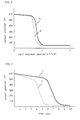
- Characteristics of the photosensitive member were determined by measuring surface potential by means of a surface potentiometer provided at the location of the image development means to detect the repetition of dark parts and light parts, while the light exposure amount by the laser ray was varied. The results are shown in Fig. 6.
- the initial characteristic is represented by the curve A
- the characteristic after 10,000 times of image formation according to the present invention is represented by the curve B
- the characteristic after 10,000 times of image formation according to the conventional method is represented by the curve C.
- Fig. 7 the initial characteristic of dark decay is represented by the curve A
- the dark decay of the photosensitive member after 10,000 times of image formation according to the present invention is represented by the curve B
- the dark decay of the photosensitive member after 10,000 times of image formation according to the conventional method is represented by the curve C.
- the surface potential decay was small even after 3 to 5 minutes in the photosensitive member after 10,000 times of image formation according to the present invention (B), whereas it fell within about 30 seconds in the photosensitive member after 10,000 times of image formation according to the conventional method (C). This suggests that the image-forming apparatus of the present invention can cope with a slower electric signal processing speed to be employed to obtain higher resolution.
- Image formation was further repeated 50,000 times according to the method of the present invention, and sensitivity characteristic and dark decay of the photosensitive member were measured. As a result, while shift of about 0.2 ⁇ J/cm 2 was observed for the sensitivity characteristic, image quality was not substantially affected because of the high gamma for latent image of the photosensitive member. The dark decay gradually became faster, and was around 2 seconds after 50,000 times of image formation, but it did not change but stayed constant thereafter.
- Example 2 The same photosensitive member as used in Example 1 was used in an image-forming apparatus provided with a contact electrifier and light exposure means for charge erasing as shown in Fig. 3, and image formation was performed using a semiconductor laser having a wavelength of 780 nm at 1200 DPI to examine the sensitivity characteristic of the photosensitive member and image stability.
- the contact electrifier was provided with a rayon brush subjected to conducting treatment (pile length: 5.0 mm, fiber density: 56,000 F/25 mm 2 , resistivity: 1.2 ⁇ 10 8 ⁇ cm), and it was installed so that brush length pressed onto the photosensitive member would be 1.0 mm.
- the contact electrifier generated an alternating current electric field of 500 Hz (applied voltage: 1.5 kV).
- the charge erasing light source was installed in such a manner that the light exposure was performed at a location immediately before the contact electrifier, and the light exposure was performed while cutting light of a wavelength of 600 nm or less by the filter 10.
- Sensitivity characteristic of the photosensitive member was determined by measuring surface potential by means of a surface potentiometer provided at the location of the image development means to detect the repetition of dark parts and light parts, while the light exposure amount by the laser ray was varied. The results are shown in Fig. 8. In Fig. 8, the initial characteristic is represented by the curve A, and the characteristic after 10,000 times of image formation in this example is represented by the curve B.
- the image-forming apparatus and the image-forming method of the present invention effective and uniform charge erasing can be realized in electrophotographic image formation utilizing a high-gamma photosensitive member. Accordingly, they can prevent so-called hysteresis and sensitivity shift even in continuous image formation, and can provide stable image formation with high quality and high resolution without residual images.
Landscapes
- Physics & Mathematics (AREA)
- General Physics & Mathematics (AREA)
- Discharging, Photosensitive Material Shape In Electrophotography (AREA)
- Photoreceptors In Electrophotography (AREA)
Applications Claiming Priority (3)
| Application Number | Priority Date | Filing Date | Title |
|---|---|---|---|
| JP8046397 | 1997-03-31 | ||
| JP8046397 | 1997-03-31 | ||
| PCT/JP1998/001345 WO1998044393A1 (fr) | 1997-03-31 | 1998-03-26 | Dispositif de formation d'images et procede de formation d'images utilisant l'electrophotographie |
Publications (2)
| Publication Number | Publication Date |
|---|---|
| EP0973074A1 true EP0973074A1 (fr) | 2000-01-19 |
| EP0973074A4 EP0973074A4 (fr) | 2002-04-17 |
Family
ID=13718964
Family Applications (1)
| Application Number | Title | Priority Date | Filing Date |
|---|---|---|---|
| EP98911015A Withdrawn EP0973074A4 (fr) | 1997-03-31 | 1998-03-26 | Dispositif de formation d'images et procede de formation d'images utilisant l'electrophotographie |
Country Status (3)
| Country | Link |
|---|---|
| US (1) | US6233416B1 (fr) |
| EP (1) | EP0973074A4 (fr) |
| WO (1) | WO1998044393A1 (fr) |
Families Citing this family (9)
| Publication number | Priority date | Publication date | Assignee | Title |
|---|---|---|---|---|
| JP2003215891A (ja) * | 2002-01-25 | 2003-07-30 | Sharp Corp | 帯電装置 |
| JP4118103B2 (ja) * | 2002-08-27 | 2008-07-16 | 株式会社沖データ | 画像形成装置 |
| JP2005189799A (ja) * | 2003-12-05 | 2005-07-14 | Ricoh Co Ltd | 画像形成装置、画像形成方法及びプロセスカートリッジ |
| US7424250B2 (en) * | 2005-12-28 | 2008-09-09 | Xerox Corporation | Methods and devices for removing latent image ghosts photoreceptors |
| US7848679B2 (en) * | 2007-12-26 | 2010-12-07 | Canon Kabushiki Kaisha | Image forming apparatus |
| JP6402989B2 (ja) * | 2014-07-25 | 2018-10-10 | 株式会社リコー | 画像形成装置 |
| JP6511361B2 (ja) * | 2015-08-03 | 2019-05-15 | シャープ株式会社 | 画像形成装置及び画像形成方法 |
| JP6724805B2 (ja) * | 2016-03-31 | 2020-07-15 | 京セラドキュメントソリューションズ株式会社 | 画像形成装置、除電部材 |
| JP2018180425A (ja) * | 2017-04-20 | 2018-11-15 | 富士ゼロックス株式会社 | 画像形成装置 |
Family Cites Families (13)
| Publication number | Priority date | Publication date | Assignee | Title |
|---|---|---|---|---|
| JPS5264936A (en) * | 1975-11-25 | 1977-05-28 | Canon Inc | Apparatus for electronic photography |
| JPS5593186A (en) * | 1979-01-08 | 1980-07-15 | Matsushita Electric Ind Co Ltd | Electrostatic transfer type copying machine |
| US4413897A (en) * | 1979-10-31 | 1983-11-08 | Tokyo Shibaura Denki Kabushiki Kaisha | Electrostatic copying apparatus |
| JPS56102882A (en) * | 1980-01-18 | 1981-08-17 | Toshiba Corp | Electrophotographic copier |
| DE3536836A1 (de) * | 1984-10-17 | 1986-04-17 | Sharp K.K., Osaka | Entladevorrichtung fuer ein kopiergeraet |
| JPS61165764A (ja) * | 1985-01-17 | 1986-07-26 | Sharp Corp | 電子写真プロセス |
| JP3125192B2 (ja) * | 1990-05-21 | 2001-01-15 | コニカ株式会社 | 画像形成方法 |
| JPH04337735A (ja) * | 1991-05-15 | 1992-11-25 | Seiko Epson Corp | 画像形成装置 |
| JPH06348111A (ja) * | 1993-06-08 | 1994-12-22 | Mitsubishi Petrochem Co Ltd | 画像形成方法 |
| JP3133565B2 (ja) * | 1993-07-08 | 2001-02-13 | キヤノン株式会社 | 画像形成装置 |
| US5652649A (en) * | 1994-11-08 | 1997-07-29 | Minolta Co., Ltd | Charging device and image forming apparatus |
| JPH09179386A (ja) * | 1995-12-27 | 1997-07-11 | Fuji Xerox Co Ltd | 画像形成装置 |
| JPH09222779A (ja) * | 1996-02-16 | 1997-08-26 | Fuji Xerox Co Ltd | 画像形成装置 |
-
1998
- 1998-03-26 US US09/381,854 patent/US6233416B1/en not_active Expired - Fee Related
- 1998-03-26 EP EP98911015A patent/EP0973074A4/fr not_active Withdrawn
- 1998-03-26 WO PCT/JP1998/001345 patent/WO1998044393A1/fr not_active Ceased
Also Published As
| Publication number | Publication date |
|---|---|
| WO1998044393A1 (fr) | 1998-10-08 |
| EP0973074A4 (fr) | 2002-04-17 |
| US6233416B1 (en) | 2001-05-15 |
Similar Documents
| Publication | Publication Date | Title |
|---|---|---|
| US3866574A (en) | Xerographic developing apparatus | |
| US4545669A (en) | Low voltage electrophotography with simultaneous photoreceptor charging, exposure and development | |
| DE3851278T2 (de) | Bilderzeugungsgerät. | |
| US6233416B1 (en) | Electrophotography with AC erasing of latent image | |
| US4391502A (en) | Electrophotographic apparatus having means for adjusting the reproduction properties of subsequent copies after a first copy has been produced | |
| JPS61277977A (ja) | 画像形成装置 | |
| EP0240888A2 (fr) | Méthode et appareil d'électrophotographie en couleurs | |
| JP2608308B2 (ja) | コロナ帯電装置におけるペパー・トラッキングを防止する方法 | |
| JP3131353B2 (ja) | 感光体寿命検知装置およびこれを備えた画像形成装置 | |
| EP0216374B1 (fr) | Appareil électrophotographique à couleurs | |
| US6035162A (en) | Charging device and image forming apparatus | |
| JPH02264278A (ja) | 画像形成装置 | |
| JPS60249166A (ja) | 電子写真の画像濃度調整方法 | |
| JP2005062737A (ja) | 画像形成装置 | |
| DE69011248T2 (de) | Elektrostatografisches Gerät. | |
| JP3155793B2 (ja) | 現像装置 | |
| JPH0727297B2 (ja) | 表面電位測定装置 | |
| JP3146272B2 (ja) | 画像形成方法 | |
| JP3249325B2 (ja) | 画像形成装置 | |
| JPS6013174B2 (ja) | 複数枚複写方法 | |
| US4329414A (en) | Electrophotographic process | |
| JP2801230B2 (ja) | 画像形成装置 | |
| JPWO1998044393A1 (ja) | 電子写真法を用いた画像形成装置及び画像形成方法 | |
| JPH0511306B2 (fr) | ||
| JPH08190325A (ja) | 画像形成装置 |
Legal Events
| Date | Code | Title | Description |
|---|---|---|---|
| PUAI | Public reference made under article 153(3) epc to a published international application that has entered the european phase |
Free format text: ORIGINAL CODE: 0009012 |
|
| 17P | Request for examination filed |
Effective date: 19991027 |
|
| AK | Designated contracting states |
Kind code of ref document: A1 Designated state(s): GB |
|
| A4 | Supplementary search report drawn up and despatched |
Effective date: 20020307 |
|
| AK | Designated contracting states |
Kind code of ref document: A4 Designated state(s): GB |
|
| RIC1 | Information provided on ipc code assigned before grant |
Free format text: 7G 03G 21/00 A, 7G 03G 15/00 B, 7G 03G 21/06 B |
|
| 17Q | First examination report despatched |
Effective date: 20040423 |
|
| STAA | Information on the status of an ep patent application or granted ep patent |
Free format text: STATUS: THE APPLICATION IS DEEMED TO BE WITHDRAWN |
|
| 18D | Application deemed to be withdrawn |
Effective date: 20040905 |