EP0973229B1 - Antenne für dritte Resonanz - Google Patents
Antenne für dritte Resonanz Download PDFInfo
- Publication number
- EP0973229B1 EP0973229B1 EP98111290A EP98111290A EP0973229B1 EP 0973229 B1 EP0973229 B1 EP 0973229B1 EP 98111290 A EP98111290 A EP 98111290A EP 98111290 A EP98111290 A EP 98111290A EP 0973229 B1 EP0973229 B1 EP 0973229B1
- Authority
- EP
- European Patent Office
- Prior art keywords
- antenna
- antenna element
- oblong
- distance
- antenna according
- Prior art date
- Legal status (The legal status is an assumption and is not a legal conclusion. Google has not performed a legal analysis and makes no representation as to the accuracy of the status listed.)
- Expired - Lifetime
Links
- 239000000758 substrate Substances 0.000 claims description 29
- 239000000126 substance Substances 0.000 claims description 19
- 239000002184 metal Substances 0.000 claims description 15
- 230000005540 biological transmission Effects 0.000 claims description 14
- 239000006260 foam Substances 0.000 claims description 2
- 238000010586 diagram Methods 0.000 description 11
- 239000000463 material Substances 0.000 description 9
- 229920005830 Polyurethane Foam Polymers 0.000 description 5
- 239000011496 polyurethane foam Substances 0.000 description 5
- 238000003491 array Methods 0.000 description 3
- 230000005404 monopole Effects 0.000 description 3
- 239000007769 metal material Substances 0.000 description 2
- 230000003044 adaptive effect Effects 0.000 description 1
- 239000000470 constituent Substances 0.000 description 1
- 230000003071 parasitic effect Effects 0.000 description 1
- 230000005855 radiation Effects 0.000 description 1
Images


Classifications
-
- H—ELECTRICITY
- H01—ELECTRIC ELEMENTS
- H01Q—ANTENNAS, i.e. RADIO AERIALS
- H01Q21/00—Antenna arrays or systems
- H01Q21/06—Arrays of individually energised antenna units similarly polarised and spaced apart
- H01Q21/08—Arrays of individually energised antenna units similarly polarised and spaced apart the units being spaced along or adjacent to a rectilinear path
- H01Q21/12—Parallel arrangements of substantially straight elongated conductive units
-
- H—ELECTRICITY
- H01—ELECTRIC ELEMENTS
- H01Q—ANTENNAS, i.e. RADIO AERIALS
- H01Q1/00—Details of, or arrangements associated with, antennas
- H01Q1/36—Structural form of radiating elements, e.g. cone, spiral, umbrella; Particular materials used therewith
- H01Q1/38—Structural form of radiating elements, e.g. cone, spiral, umbrella; Particular materials used therewith formed by a conductive layer on an insulating support
-
- H—ELECTRICITY
- H01—ELECTRIC ELEMENTS
- H01Q—ANTENNAS, i.e. RADIO AERIALS
- H01Q21/00—Antenna arrays or systems
- H01Q21/06—Arrays of individually energised antenna units similarly polarised and spaced apart
- H01Q21/08—Arrays of individually energised antenna units similarly polarised and spaced apart the units being spaced along or adjacent to a rectilinear path
-
- H—ELECTRICITY
- H01—ELECTRIC ELEMENTS
- H01Q—ANTENNAS, i.e. RADIO AERIALS
- H01Q21/00—Antenna arrays or systems
- H01Q21/06—Arrays of individually energised antenna units similarly polarised and spaced apart
- H01Q21/20—Arrays of individually energised antenna units similarly polarised and spaced apart the units being spaced along or adjacent to a curvilinear path
- H01Q21/205—Arrays of individually energised antenna units similarly polarised and spaced apart the units being spaced along or adjacent to a curvilinear path providing an omnidirectional coverage
-
- H—ELECTRICITY
- H01—ELECTRIC ELEMENTS
- H01Q—ANTENNAS, i.e. RADIO AERIALS
- H01Q9/00—Electrically-short antennas having dimensions not more than twice the operating wavelength and consisting of conductive active radiating elements
- H01Q9/04—Resonant antennas
- H01Q9/06—Details
-
- H—ELECTRICITY
- H01—ELECTRIC ELEMENTS
- H01Q—ANTENNAS, i.e. RADIO AERIALS
- H01Q9/00—Electrically-short antennas having dimensions not more than twice the operating wavelength and consisting of conductive active radiating elements
- H01Q9/04—Resonant antennas
- H01Q9/16—Resonant antennas with feed intermediate between the extremities of the antenna, e.g. centre-fed dipole
- H01Q9/28—Conical, cylindrical, cage, strip, gauze, or like elements having an extended radiating surface; Elements comprising two conical surfaces having collinear axes and adjacent apices and fed by two-conductor transmission lines
Definitions
- the present invention relates to an antenna which is particularly adapted for radiating near or at the third resonance.
- the antenna comprises a reflector means, e.g. a reflector plate.
- Printed dipole antennas with reflector plates are e.g. described in the US-patent no. 3587110, which discloses the idea of printed antenna structures over a reflector plane.
- the described dipoles radiate in first resonance.
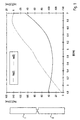
- Fig. 1 an example for a known dipole antenna comprising two antenna elements is shown on the left side of the figure whereas the real and the imaginary part of the impedance of this dipole antenna is shown on the right side of the figure.
- the two dipole elements 1, 2 have an oblong shape and are arranged opposite to each other. In other words, the two antenna elements 1 and 2 are positioned on the same longitudinal axis in the same plane. The antenna elements 1 and 2 are fed at their respective ends, which are close to each other.
- Dipole antennas printed on a dielectric substrate with a reflection plate being arranged at a certain distance to said dielectric substrate have a number of advantages over conventional microstrip patch antennas. The main advantages are the wider bandwidth, lower loss and less parasitic radiation of the feeding or transmission lines.
- the distance between the reflection plate and the dielectric substrate is advantageously set to ⁇ /4, whereby ⁇ is the electric wave length of the central frequency within the material between the reflector plate and the dielectric substrate.
- dipole antennas radiating at the first resonance with an impedance near 50 Ohms have been used, as well as dipole antennas radiating at the second resonance, the impedances of which are of a magnitude of several hundred Ohms for a parallel connection in antenna arrays.
- the gain of dipole antennas radiating at the first resonance with a reflector plate arranged at a distance of ⁇ /4 is about 7.5 dB and the gain of dipole antennas radiating at the second resonance is about 8 dB.
- dipole antennas radiating on the third resonance due to their comparatively high electrical wavelength, have a gain of around 10 dB.
- VSWR high voltage standing wave ratio
- the imaginary part Im[Z] of the impedance Z has a negative value, i.e. it has a capacitance character. It becomes clear from Fig. 1 that in this case the input impedance is not ideal.
- WO 88/09065 discloses a device for receiving and/or transmitting electromagnetic signals in a broad frequency range from 33 MHz to 1042 MHz which is formed by a planar element having an array of constituent planar plates arranged in a configuration such that the planar element is symmetrical about at least one axis with each of the plate members being connected either indirectly or directly to, or continuous with, the other plate members.
- One significant feature of the respective planar antenna element is an enlarged capture and transmission area for electromagnetic waves on the front and rear faces of the plates.
- the object of the present invention is therefore to provide an antenna radiating at the third resonance, the impedance of which can be matched easily to the impedance of the feeding system.
- an antenna according to claim 1 with a first antenna element comprising a first and a second oblong portion arranged parallel and with a distance to each other, a transverse portion connecting said first and said second oblong portion at a distance from a feeding side end of said first and second oblong portion and a feeding portion extending parallel to and between said first and said second oblong portion for connecting said transverse portion with a transmission line, and a reflector means spaced to and parallel with a common plane of said first and said second oblong portion.
- the antenna according to the present invention is adopted to radiate at the third resonance, which means a larger gain compared to conventional antennas radiating at at the first and the second resonance is provided. Simultaneously, the antenna according to the present invention has good matching capabilities. In other words, the antenna according to the present invention can easily be shaped to have an impedance close to the impedance of the feeding system, e. g. 50 Ohms. A further advantage of the antenna according to the present invention is the measured working band width of 10 % for a VSWR smaller than 2.
- the antenna according to the present invention when used as a dipole antenna, can be readily adapted for being arranged in antenna arrays, when a band width of 40-50 degrees in the E-plane is needed as well as in phase scanned arrays and smart antennas.
- a second antenna element is arranged opposite to said first antenna element and comprises a first and a second oblong portion arranged parallel and with a distance to each other.
- said second antenna element is positioned on the same longitudinal axis and in the same plane as said first antenna element.
- a transverse portion connects said first and second oblong portion at a distance from a feeding side end of said first and second oblong portion and a feeding portion extends parallel to and between said first and said second oblong portion for connecting said transverse portion with a transmission line.
- Said reflector means is commonly used for said first and said second antenna element and is spaced to and parallel with a common plane of said first and said second oblong portion of said second antenna element.
- the first antenna element and the second antenna element arranged opposite to each other operate as a dipole antenna.
- the reflector means advantageously is a reflector plate consisting of a metal material.
- the distance L2 is smaller than L/2 whereby L is the length of the first and the second oblong portion. This means that the transverse portion is located closer to the feeding side end of the first and/or second antenna element than to the end opposite to said feeding side end.
- a distance S between said feeding portion at said first and said second oblong portion is smaller than W2/2, respectively.
- said low loss substance is air. This means that no material is located between the first and/or second antenna element and the reflector means.
- said low loss substance can be a synthetic foam, e.g. polyurethane foam.
- said first and/or said second antenna element consist(s) of thin metal plates, e.g. if the low loss substance is air.
- said first and/or said second antenna element consist(s) of thin metal films printed on a dielectric substrate.
- the antenna is a dipole antenna comprising a first and a second antenna element
- the first and the second antenna element can be printed on the same face of said dielectric substrate.
- said first and said second antenna element can be printed onto opposite faces of said dielectric substrate.
- the antenna according to the present invention is a dipole antenna comprising a first and a second antenna element
- the transmission lines can be balanced microstrip lines. In this case.
- the balanced microstrip lines can be coplanar to said first and to said second antenna element, respectively.
- said balanced microstrip lines can be essentially orthogonal to said first and said second antenna element.
- a plurality of antennas comprising a first and a second antenna element can be arranged in an antenna array to be used as a diversity antenna, a phase scanned array or a smart antenna.
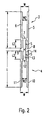
- Fig. 2 shows an example for an antenna according to the present invention.
- the shown antenna comprises a first antenna element 3 and a second antenna element 4 arranged opposite to each other on the same longitudinal axis and extending in a common plane.
- the shown antenna operates as a dipole antenna.
- the first antenna element comprises a first and a second oblong portion 5, 6.
- the first and the second oblong portion 5, 6 are arranged parallel and with a distance W2 to each other.
- the first and the second oblong portion 5, 6 thereby have the same length and the same width.
- a transverse portion 7 connects said first and said second oblong portion 5, 6 at a distance L2 from a feeding side and 9 of said first and said second oblong portion 5, 6.
- the feeding side end 9 of the first antenna element is the end of the antenna element on which the antenna element is fed.
- the first antenna element 3 further comprises a feeding portion 8 extending parallel to and between said first and said second oblong portion 5, 6.
- the feeding portion 8 is connected to said transverse portion 7 and extends parallel to and in a common plane with said first and said second oblong portion, whereby a respective slot is formed between said feeding portion 8 and said first and said second oblong portion 5, 6, respectively.
- the width of said slot or the distance between said feeding portion and said first and said second oblong portion 5, 6, respectively, has a value S.
- the value S is set to be smaller than W/2, whereby W is the entire width of the first antenna element.
- the distance L2 between said transverse portion 7 and said feeding side end 9 is smaller than L/2 whereby L is the overall length of the first and the second oblong portion 5, 6.
- the second antenna element 4 arranged opposite to said first antenna element 3 has exactly the same shape and measures as the first antenna element 3.
- the second antenna element 4 comprises a first and a second oblong portion 10, 11 arranged parallel and with a distance W2 to each other.
- the first and the second oblong portion 10, 11 have the same length L.
- a transverse portion 12 connects said first and said second oblong portion 10, 11, at a distance L2 from a feeding side end 14 of said first and said second oblong portion 10, 11.
- a feeding portion 13 extends parallel to and between said first and said second oblong portion 10, 11.
- the width S of the slots between the feeding portion 13 and said first and said second oblong portion 10, 11, respectively, is smaller than W/2, whereby W is the width of said second antenna element.
- L2 is smaller than L/2 whereby L is the overall length of said first and said second oblong portion 10, 11.
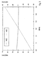
- the real part Re[Z] of the input impedance Z of the antenna can be minimized so that a very good matching with the feeding system impedance can be achieved, which is shown in Fig. 3.
- the dimensions of the first and/or the second antenna element 3, 4 it is possible to perform a fine tuning of the antenna impedance to the desired value.
- a frequency diagram of the real part Re[Z] and the imaginary part Im[Z] of the input impedance Z of the antenna is shown for the dipole antenna shown in Fig. 2.
- the basic shape and measures of the shown antenna elements 3, 4 is essentially the same as the shape of the antenna elements 3, 4 shown in Fig. 2.
- Fig. 4 another example of a dipole antenna comprising a first antenna element 3 and a second antenna element 4 arranged opposite to each other is shown.
- the two antenna elements are printed onto the same side of a dielectric substrate 17.
- the dielectric substrate 17 is mounted onto a low loss material 16, which e.g. is a polyurethane foam.
- a reflector plate 15 is located on the other side of the low loss material 16.
- the distance H between the reflector plate 15 and the dielectric substrate 17 on which the antenna elements 3, 4 are printed, is ⁇ /4, whereby ⁇ is the electric wavelength of the center frequency within the low loss material 16.
- Low loss means that the material 16 has a dielectric constant of about 1.
- the first and the second antenna element 3, 4 are connected to and fed by microstrip lines 18.
- the microstrip lines 18 are printed onto a support plate 19.
- the microstrip lines 18 extend orthogonal to the common plane of the first and the second antenna element 3.
- the feeding side ends 9, 14, which are the ends of the first and the second antenna element 3, 4, which are close to each other, are connected to the microstrip lines 18.
- the microstrip lines 18 are balanced microstrips, which change into unbalanced microstrips in direction to the SMA connector 20.
- the microstrip lines 18 extend in the same plane as the first and the second antenna element 3, 4, whereby the first antenna element 3 and the second antenna element 4 are printed on opposite faces of the dielectric substrate 17.
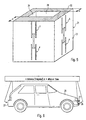
- an antenna 21 comprising a plurality of dipole antennas, each comprising a first and a second antenna element 3, 4 is shown.
- the shown antenna comprises four dipole antennas.
- Each dipole antenna comprises a first and a second antenna element 3, 4 and is arranged on a side face of a cube.
- the first and second antenna elements 3, 4 are printed onto a dielectric substrate 23 which is located on a low loss substance 22.
- Inside the antenna a square hole is formed, the side walls of which are formed by respective reflector plates 24.
- the distance H between each reflector plate on the inside of the cube and the corresponding dipole antenna is ⁇ /4, whereby ⁇ is the electric wavelength of the center frequency in the low loss substance 22.
- the longitudinal axis of the first and the second antenna element 3, 4 of each dipole antenna shown in Fig. 5 are parallel to each other and parallel to the middle axis of the through hole formed by the four reflector plates 24.
- the antenna 21 shown in Fig. 5 operates as a diversity antenna or as a smart antenna.
- Fig. 6 the use of a dipole antennas according to the present invention in a car 25 is shown.
- Four dipole antennas 26 each comprising a first and a second dipole element 3, 4 are integrated in the four corners of a car 25.
- the antenna 26 at the right front corner of the car 25 in Fig. 6 the four antennas can be integrated into the bumpers 27 of the car.
- the longitudinal axis of the antenna 26 extends normally to the ground.
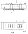
- Fig. 7 an example of an antenna array 28 comprising a plurality, e.g. 8 dipole antennas according to the present invention is shown.
- all dipole antennas each comprising a first and a second element 3, 4 are printed on the same face of a dielectric substrate 29 and are fed by balanced microstrip lines 33 extending orthogonally to the common plane of the dipole antennas.
- a reflector plate 30 At a distance H from the dielectric substrate 29, a reflector plate 30 is located. Between the dielectric substrate and the reflector plate 30, a low loss substance 35 is arranged.
- the low loss substance 35 can be air or a low loss support material, e.g. polyurethane foam.
- the distance H is chosen to be ⁇ /4 whereby ⁇ is the electrical wavelength at the center frequency and the low loss substance.
- the microstrip feeding or transmission lines 34 are balanced within the low loss substance. Between the reflector plate and the SMA connectors 32 for connecting the antenna feeding lines 33 with further transmission means, a transmission from balanced to unbalanced microstrip lines takes place within the transmission lines 34.
- the SMA connectors 32 can be fixed to a support plate 31.
- a top view of the antenna 28 shown in Fig. 7 is shown.
- Each of the 8 dipole antennas comprises a first and a second antenna element 3, 4. All the first and the second antenna elements 3, 4 are printed onto the same face of the dielectric substrate 29. All dipole antennas are arranged parallel and spaced to each other.
- the antenna array shown in Fig. 7 and 8 can be used as smart antenna, fixed phase antenna or adaptive phase antenna.
- the antenna elements consist of thin metal films which are printed onto a dielectric substrate.
- an antenna according to the present invention is shown, which consists of thin metal plates which are not printed onto any substrate and extend freely.
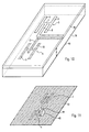
- the antenna shown in Fig. 9 is realized as a monopole antenna comprising only one antenna element 3.
- a reflector plate 36 is located at a distance H and parallel to the antenna element 3.
- the low loss substance is air.
- the antenna element 3 is mounted onto a support plane 37 extending orthogonal to the reflector plate 36.
- the antenna element 3 of the monopole antenna shown in Fig. 9 can also be printed onto a dielectric substrate, whereby the electric substrate can either be mounted onto a low loss substance, e.g. polyurethane foam, or extend freely.
- a dipole antenna comprising a first and a second antenna element 3, 4
- the first antenna element 3 is printed as a thin metal film onto an upper face of a dielectric substrate 38
- the second antenna element 4 is printed as thin metal film onto the lower face of the dielectric substrate 38.
- the dielectric substrate is located on a low loss substance 39, which can e.g. be polyurethane foam or air.
- the first and the second antenna element 3, 4 are fed by balanced microstrip lines, which extend in the same plane as the respective antenna element 3, 4.
- a dipole antenna comprising a first and a second antenna element 3, 4
- the first and the second element consist of thin metal plates with a finite thickness, which extend freely.
- the low loss material located between the first and the second element 3, 4 and the reflector plate 43 is air.
- the first and the second antenna element are fed by balanced metal strip lines 44, 45 extending orthogonal to the common plane of the first and the second antenna element 3, 4.
- the metal strip lines 44, 45 consist of metal with a finite thickness.
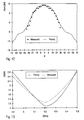
- Fig. 12 shows the measured and the predicted antenna gain for the embodiment shown in Fig. 4. From the diagram it can be seen, that the maximum antenna gain is about 9.5 dBi, which means that the antenna according to the present invention radiating at the third resonance provides a much higher antenna gain than known antennas radiating at the first and the second resonance.
- Fig. 13 the calculated and measured values of the VSWR for one dipole antenna of the antenna array shown in Fig. 7 and 8 is shown. It can be seen, that one dipole antenna in the antenna array of Fig. 7 and 8 has an operation bandwidth of 8 % for a VSWR less than two.
- the reflector plane or reflector plate consists of a metal material.
- the reflector plate can either be printed as a thin metal film onto a corresponding substrate, or the reflector plate can consist of a metal film with a finite thickness.
Landscapes
- Variable-Direction Aerials And Aerial Arrays (AREA)
- Details Of Aerials (AREA)
- Aerials With Secondary Devices (AREA)
Claims (14)
- Antenne, mit:dadurch gekennzeichnet, dasseinem ersten Antennenelement (3), welches einen ersten und einen zweiten länglichen Bereich (5, 6) aufweist, die parallel und mit einem Abstand W2 zueinander angeordnet sind, einen Querbereich (7), der den ersten und den zweiten länglichen Bereich (5, 6) in einem Abstand L2 von dem speiseseitigen Ende (9) des ersten und des zweiten länglichen Bereichs (5, 6) verbindet, und einen Speisebereich, der sich parallel zu und zwischen dem ersten und dem zweiten langgestreckten Bereich (5, 6) erstreckt, um den Querbereich (7) mit einer Übertragungsleitung zu verbinden, und einer Reflektoreinrichtung (15, 24, 31, 36, 40, 43), die parallel beabstandet zu einer gemeinsamen Ebene des ersten und des zweiten langgestreckten Bereichs ist,
L2 kleiner ist als L/2, wobei L die Länge des ersten und des zweiten langgestreckten Bereichs (5, 6; 10, 11) ist. - Antenne nach Anspruch 1,
gekennzeichnet durch
ein zweites Antennenelement (4), welches gegenüber dem ersten Antennenelement (3) angeordnet ist und einen ersten und zweiten langgestreckten Bereich (10, 11) aufweist, die parallel und mit einem Abstand W2 zueinander angeordnet sind, einen Querbereich (12), der den ersten und den zweiten langgestreckten Bereich (10, 11) in einem Abstand L2 von dem speiseseitigen Ende (14) des ersten und des zweiten langgestreckten Bereichs (10, 11) verbindet, und einen Speisebereich (13), der sich parallel zu und zwischen dem ersten und dem zweiten langgestreckten Bereich (10, 11) erstreckt, um den Querbereich (12) mit einer Übertragungsleitung zu verbinden, wobei die Reflektoreinrichtung (15) beabstandet zu und parallel mit einer gemeinsamen Ebene des ersten und des zweiten langgestreckten Bereichs (10, 11) des zweiten Antennenelements (4) ist. - Antenne nach Anspruch 1 oder 2,
dadurch gekennzeichnet, dass
ein Abstand S zwischen dem Speisebereich und dem ersten bzw. dem zweiten langgestreckten Bereich (5, 6, 10, 11) kleiner ist als W/2. - Antenne nach Anspruch 1 , 2 oder 3,
dadurch gekennzeichnet, dass
eine Substanz (16, 22, 35, 39), das einen niedrigen Verlust hat, zwischen dem ersten und/oder zweiten Antennenelement (3, 4) und der Reflektoreinrichtung angeordnet ist und der Abstand H zwischen dem ersten und/oder dem zweiten Antennenelement und der Reflektoreinrichtung im Wesentlichen H = λ/4 beträgt, wobei λ die elektrische Wellenlänge der Mittenfrequenz innerhalb der Substanz, die niedrigen Verlust hat, ist. - Antenne nach einem der vorhergehenden Ansprüche,
dadurch gekennzeichnet, dass
die Substanz (35), die niedrigen Verlust hat, Luft ist. - Antenne nach einem der Ansprüche 1 bis 5,
dadurch gekennzeichnet, dass
die Substanz (16, 22, 39), die niedrigen Verlust hat, ein synthetischer Schaum ist. - Antenne nach einem der vorhergehenden Ansprüche,
dadurch gekennzeichnet, dass
das erste und/oder zweite Antennenelement (5, 6, 10, 11) aus dünnen Metallplatten besteht. - Antenne nach einem der Ansprüche 1 bis 7,
dadurch gekennzeichnet, dass
das erste und/oder zweite Antennenelement (5, 6; 10, 11) aus dünnen Metallfilmen besteht, die auf ein dielektrisches Substrat (17, 23, 29, 38) gedruckt sind. - Antenne nach Anspruch 8, wenn zurückbezogen auf Anspruch 2,
dadurch gekennzeichnet, dass
das erste und das zweite Antennenelement (5, 6; 10, 11) auf die gleiche Fläche des dielektrischen Substrats gedruckt sind. - Antenne nach Anspruch 8, wenn zurückbezogen auf Anspruch 2,
dadurch gekennzeichnet, dass
das erste und das zweite Antennenelement (5, 6; 10, 11) auf gegenüberliegenden Flächen des dielektrischen Substrats gedruckt sind. - Antenne nach einem der Ansprüche 3 bis 10, wenn zurückbezogen auf Anspruch 2,
dadurch gekennzeichnet, dass
die Übertragungsleitungen symmetrische Mikrostrip-Leitungen sind. - Antenne nach Anspruch 11,
dadurch gekennzeichnet, dass
die symmetrischen Mikrostrip-Leitungen zum ersten bzw. zweiten Antennenelement (5, 6; 10, 11) koplanar sind. - Antenne nach Anspruch 11,
dadurch gekennzeichnet, dass
die symmetrischen Mikrostrip-Leitungen im Wesentlichen orthogonal zum ersten und zweiten Antennenelement sind. - Antennenbaugruppe, die mehrere Antennen aufweist, wie in einem der Ansprüche 3 bis 13 definiert, wenn zurückbezogen auf Anspruch 2.
Priority Applications (2)
| Application Number | Priority Date | Filing Date | Title |
|---|---|---|---|
| DE69830236T DE69830236T2 (de) | 1998-06-18 | 1998-06-18 | Antenne für dritte Resonanz |
| EP98111290A EP0973229B1 (de) | 1998-06-18 | 1998-06-18 | Antenne für dritte Resonanz |
Applications Claiming Priority (1)
| Application Number | Priority Date | Filing Date | Title |
|---|---|---|---|
| EP98111290A EP0973229B1 (de) | 1998-06-18 | 1998-06-18 | Antenne für dritte Resonanz |
Publications (2)
| Publication Number | Publication Date |
|---|---|
| EP0973229A1 EP0973229A1 (de) | 2000-01-19 |
| EP0973229B1 true EP0973229B1 (de) | 2005-05-18 |
Family
ID=8232143
Family Applications (1)
| Application Number | Title | Priority Date | Filing Date |
|---|---|---|---|
| EP98111290A Expired - Lifetime EP0973229B1 (de) | 1998-06-18 | 1998-06-18 | Antenne für dritte Resonanz |
Country Status (2)
| Country | Link |
|---|---|
| EP (1) | EP0973229B1 (de) |
| DE (1) | DE69830236T2 (de) |
Citations (2)
| Publication number | Priority date | Publication date | Assignee | Title |
|---|---|---|---|---|
| US4719470A (en) * | 1985-05-13 | 1988-01-12 | Ball Corporation | Broadband printed circuit antenna with direct feed |
| WO1988009065A1 (en) * | 1987-05-08 | 1988-11-17 | Darrell Coleman | Broad frequency range aerial |
Family Cites Families (5)
| Publication number | Priority date | Publication date | Assignee | Title |
|---|---|---|---|---|
| US3369245A (en) * | 1964-12-10 | 1968-02-13 | Technical Appliance Corp | Wing type dipole with end mounted stubs |
| US3587110A (en) * | 1969-07-01 | 1971-06-22 | Rca Corp | Corporate-network printed antenna system |
| US3747114A (en) * | 1972-02-18 | 1973-07-17 | Textron Inc | Planar dipole array mounted on dielectric substrate |
| US4074270A (en) * | 1976-08-09 | 1978-02-14 | The United States Of America As Represented By The Secretary Of The Navy | Multiple frequency microstrip antenna assembly |
| NL9401429A (nl) * | 1994-09-02 | 1996-04-01 | Hollandse Signaalapparaten Bv | Striplijn antenne. |
-
1998
- 1998-06-18 DE DE69830236T patent/DE69830236T2/de not_active Expired - Lifetime
- 1998-06-18 EP EP98111290A patent/EP0973229B1/de not_active Expired - Lifetime
Patent Citations (2)
| Publication number | Priority date | Publication date | Assignee | Title |
|---|---|---|---|---|
| US4719470A (en) * | 1985-05-13 | 1988-01-12 | Ball Corporation | Broadband printed circuit antenna with direct feed |
| WO1988009065A1 (en) * | 1987-05-08 | 1988-11-17 | Darrell Coleman | Broad frequency range aerial |
Also Published As
| Publication number | Publication date |
|---|---|
| EP0973229A1 (de) | 2000-01-19 |
| DE69830236T2 (de) | 2006-01-26 |
| DE69830236D1 (de) | 2005-06-23 |
Similar Documents
| Publication | Publication Date | Title |
|---|---|---|
| US6281843B1 (en) | Planar broadband dipole antenna for linearly polarized waves | |
| US7099686B2 (en) | Microstrip patch antenna having high gain and wideband | |
| US10854994B2 (en) | Broadband phased array antenna system with hybrid radiating elements | |
| US5070340A (en) | Broadband microstrip-fed antenna | |
| US6759990B2 (en) | Compact antenna with circular polarization | |
| US5828340A (en) | Wideband sub-wavelength antenna | |
| US7541997B2 (en) | Loaded antenna | |
| US6054953A (en) | Dual band antenna | |
| US8149171B2 (en) | Miniature antenna having a volumetric structure | |
| US6326927B1 (en) | Capacitively-tuned broadband antenna structure | |
| KR100526585B1 (ko) | 이중 편파 특성을 갖는 평판형 안테나 | |
| EP2908380B1 (de) | Breitbandige doppelt polarisierte Patch-Antennenanordnung und Verfahren in Verbindung damit | |
| US9755314B2 (en) | Loaded antenna | |
| US20190305415A1 (en) | Integrated multi-standard antenna system with dual function connected array | |
| EP1038332B1 (de) | Zweibandantenne | |
| JP2862265B2 (ja) | 平面アンテナ | |
| JP4169696B2 (ja) | 高バンド幅マルチバンド・アンテナ | |
| CA2182334C (en) | Mini-cap radiating element | |
| US20080024366A1 (en) | Dual band flat antenna | |
| US6646619B2 (en) | Broadband antenna assembly of matching circuitry and ground plane conductive radiating element | |
| JP3469834B2 (ja) | 広帯域アレーアンテナ | |
| JPH0955621A (ja) | アレーアンテナ | |
| CN111600120B (zh) | 一种紧凑的低交叉极化微带天线 | |
| EP0542447B1 (de) | Ebene Plattenantenne | |
| EP0487053A1 (de) | Antenne |
Legal Events
| Date | Code | Title | Description |
|---|---|---|---|
| PUAI | Public reference made under article 153(3) epc to a published international application that has entered the european phase |
Free format text: ORIGINAL CODE: 0009012 |
|
| AK | Designated contracting states |
Kind code of ref document: A1 Designated state(s): DE FR GB |
|
| AX | Request for extension of the european patent |
Free format text: AL;LT;LV;MK;RO;SI |
|
| 17P | Request for examination filed |
Effective date: 20000522 |
|
| AKX | Designation fees paid |
Free format text: DE FR GB |
|
| RAP1 | Party data changed (applicant data changed or rights of an application transferred) |
Owner name: SONY INTERNATIONAL (EUROPE) GMBH |
|
| 17Q | First examination report despatched |
Effective date: 20040507 |
|
| GRAP | Despatch of communication of intention to grant a patent |
Free format text: ORIGINAL CODE: EPIDOSNIGR1 |
|
| GRAS | Grant fee paid |
Free format text: ORIGINAL CODE: EPIDOSNIGR3 |
|
| GRAA | (expected) grant |
Free format text: ORIGINAL CODE: 0009210 |
|
| AK | Designated contracting states |
Kind code of ref document: B1 Designated state(s): DE FR GB |
|
| REG | Reference to a national code |
Ref country code: GB Ref legal event code: FG4D |
|
| REF | Corresponds to: |
Ref document number: 69830236 Country of ref document: DE Date of ref document: 20050623 Kind code of ref document: P |
|
| RAP2 | Party data changed (patent owner data changed or rights of a patent transferred) |
Owner name: SONY DEUTSCHLAND GMBH |
|
| RAP2 | Party data changed (patent owner data changed or rights of a patent transferred) |
Owner name: SONY DEUTSCHLAND GMBH |
|
| RAP2 | Party data changed (patent owner data changed or rights of a patent transferred) |
Owner name: SONY DEUTSCHLAND GMBH |
|
| ET | Fr: translation filed | ||
| PLBE | No opposition filed within time limit |
Free format text: ORIGINAL CODE: 0009261 |
|
| STAA | Information on the status of an ep patent application or granted ep patent |
Free format text: STATUS: NO OPPOSITION FILED WITHIN TIME LIMIT |
|
| REG | Reference to a national code |
Ref country code: FR Ref legal event code: TP Ref country code: FR Ref legal event code: CA |
|
| 26N | No opposition filed |
Effective date: 20060221 |
|
| REG | Reference to a national code |
Ref country code: FR Ref legal event code: CA |
|
| REG | Reference to a national code |
Ref country code: GB Ref legal event code: 732E |
|
| PGFP | Annual fee paid to national office [announced via postgrant information from national office to epo] |
Ref country code: FR Payment date: 20110630 Year of fee payment: 14 |
|
| PGFP | Annual fee paid to national office [announced via postgrant information from national office to epo] |
Ref country code: GB Payment date: 20110620 Year of fee payment: 14 |
|
| PGFP | Annual fee paid to national office [announced via postgrant information from national office to epo] |
Ref country code: DE Payment date: 20110622 Year of fee payment: 14 |
|
| GBPC | Gb: european patent ceased through non-payment of renewal fee |
Effective date: 20120618 |
|
| REG | Reference to a national code |
Ref country code: FR Ref legal event code: ST Effective date: 20130228 |
|
| REG | Reference to a national code |
Ref country code: DE Ref legal event code: R119 Ref document number: 69830236 Country of ref document: DE Effective date: 20130101 |
|
| PG25 | Lapsed in a contracting state [announced via postgrant information from national office to epo] |
Ref country code: DE Free format text: LAPSE BECAUSE OF NON-PAYMENT OF DUE FEES Effective date: 20130101 Ref country code: GB Free format text: LAPSE BECAUSE OF NON-PAYMENT OF DUE FEES Effective date: 20120618 Ref country code: FR Free format text: LAPSE BECAUSE OF NON-PAYMENT OF DUE FEES Effective date: 20120702 |