EP0973257A2 - Filtre adapté aux ondes acoustiques de surface - Google Patents
Filtre adapté aux ondes acoustiques de surface Download PDFInfo
- Publication number
- EP0973257A2 EP0973257A2 EP19990305596 EP99305596A EP0973257A2 EP 0973257 A2 EP0973257 A2 EP 0973257A2 EP 19990305596 EP19990305596 EP 19990305596 EP 99305596 A EP99305596 A EP 99305596A EP 0973257 A2 EP0973257 A2 EP 0973257A2
- Authority
- EP
- European Patent Office
- Prior art keywords
- acoustic wave
- surface acoustic
- matched filter
- substrate
- thin film
- Prior art date
- Legal status (The legal status is an assumption and is not a legal conclusion. Google has not performed a legal analysis and makes no representation as to the accuracy of the status listed.)
- Withdrawn
Links
- 238000010897 surface acoustic wave method Methods 0.000 title claims abstract description 84
- 239000000758 substrate Substances 0.000 claims abstract description 50
- 238000001228 spectrum Methods 0.000 claims abstract description 21
- PMHQVHHXPFUNSP-UHFFFAOYSA-M copper(1+);methylsulfanylmethane;bromide Chemical compound Br[Cu].CSC PMHQVHHXPFUNSP-UHFFFAOYSA-M 0.000 claims abstract description 8
- 239000010409 thin film Substances 0.000 claims description 30
- 229910003460 diamond Inorganic materials 0.000 claims description 11
- 239000010432 diamond Substances 0.000 claims description 11
- 239000000463 material Substances 0.000 claims description 10
- XLOMVQKBTHCTTD-UHFFFAOYSA-N Zinc monoxide Chemical compound [Zn]=O XLOMVQKBTHCTTD-UHFFFAOYSA-N 0.000 claims description 8
- XUIMIQQOPSSXEZ-UHFFFAOYSA-N Silicon Chemical compound [Si] XUIMIQQOPSSXEZ-UHFFFAOYSA-N 0.000 claims description 6
- 229910052710 silicon Inorganic materials 0.000 claims description 6
- 239000010703 silicon Substances 0.000 claims description 6
- PIGFYZPCRLYGLF-UHFFFAOYSA-N Aluminum nitride Chemical compound [Al]#N PIGFYZPCRLYGLF-UHFFFAOYSA-N 0.000 claims description 3
- 230000000644 propagated effect Effects 0.000 claims description 3
- 239000011787 zinc oxide Substances 0.000 claims description 3
- TWNQGVIAIRXVLR-UHFFFAOYSA-N oxo(oxoalumanyloxy)alumane Chemical compound O=[Al]O[Al]=O TWNQGVIAIRXVLR-UHFFFAOYSA-N 0.000 claims description 2
- 229910052594 sapphire Inorganic materials 0.000 abstract description 8
- 239000010980 sapphire Substances 0.000 abstract description 8
- 238000004891 communication Methods 0.000 abstract description 7
- 238000000034 method Methods 0.000 abstract 1
- 230000003247 decreasing effect Effects 0.000 description 8
- 239000010408 film Substances 0.000 description 5
- 238000004458 analytical method Methods 0.000 description 2
- 239000013078 crystal Substances 0.000 description 2
- 238000013461 design Methods 0.000 description 2
- 238000002474 experimental method Methods 0.000 description 2
- 238000012545 processing Methods 0.000 description 2
- 230000001360 synchronised effect Effects 0.000 description 2
- 230000005540 biological transmission Effects 0.000 description 1
- 238000012986 modification Methods 0.000 description 1
- 230000004048 modification Effects 0.000 description 1
- 230000001902 propagating effect Effects 0.000 description 1
Images



Classifications
-
- H—ELECTRICITY
- H03—ELECTRONIC CIRCUITRY
- H03H—IMPEDANCE NETWORKS, e.g. RESONANT CIRCUITS; RESONATORS
- H03H9/00—Networks comprising electromechanical or electro-acoustic elements; Electromechanical resonators
- H03H9/46—Filters
- H03H9/64—Filters using surface acoustic waves
- H03H9/6406—Filters characterised by a particular frequency characteristic
- H03H9/6416—SAW matched filters, e.g. surface acoustic wave compressors, chirped or coded surface acoustic wave filters
Definitions
- Figs. 1A-1E are schematic views for explaining the general operation of such a spread spectrum communication.
- Fig. 1A illustrates a base band signal to be transmitted, and a data rate of the base band signal is denoted by f 2 (bits/sec).
- a code "1" is denoted by "11001” and a code "0" by "00110” as depicted in Fig. 1B.
- the PN code has a chip rate of f 1 .
- a spread spectrum signal shown in Fig. 1C can be obtained. Therefore, the spread spectrum signal has a center frequency of f 0 .
- the thus obtained spread spectrum signal is transmitted over a transmission path, and is supplied to an input side electrode 2 of a surface acoustic wave matched filter 1 as shown in Fig. 1D.
- the input side electrode 2 converts the received spread spectrum signal into a surface acoustic wave.
- the surface acoustic wave matched filter 1 further comprises an output side electrode 3 from which a demodulated signal may be obtained.
- the output side electrode 3 constituting the tapped delay line is designed such that the tap distance L is equal to v/f 1 .
- the velocity v of the surface acoustic wave is a phase velocity.
- the phase velocity may be defined as a velocity at which a sinusoidal wave having a single frequency propagates along the surface of the substrate 1.
- the synchronization between the output side electrode 3 and the input spread spectrum signal could not be sometimes attained and a correlation peak level of the output signal might be decreased.
- the inventors have conducted various experiments and analyses for the above mentioned decrease in the correlation peak level, and have found that the tap distance of the matched filter is designed on the basis of the phase velocity of the surface acoustic wave.
- the substrate of the surface acoustic wave matched filter has been made of various materials.
- a laminated type substrate has been developed.
- the substrate is composed of a main body made of a material such as sapphire and diamond having a higher velocity for the surface acoustic wave, and a thin film applied on the main body and made of a piezoelectric material such as aluminum nitride and zinc oxide.
- a decrease in the correlation peak level has been remarkably observed.
- the inventors have further investigated such a phenomenon, and has found that the above mentioned decrease in the correlation peak level occurs by the following reason.
- the known substrate made of a single crystal is substantially non-dispersive, but the thin film laminated type substrate has a dispersive characteristic which depends on the film thickness.
- the surface acoustic wave propagates along the surface of the substrate predominantly at the group velocity, instead of the phase velocity. Therefore, when the surface acoustic wave matched filter having the thin film laminated type substrate is designed under the phase velocity, the spread spectrum signal could not be detected in a synchronous manner by the output side electrode, and thus the correlation peak level is decreased.
- the present invention has for its object to provide a novel and useful surface acoustic wave matched filter, in which the above mentioned problems of the known filters can be removed or mitigated, and the undesired decrease in the correlation peak level of the output demodulated signal due to the dispersity of the piezoelectric substrate can be effectively removed without using the complicated and expensive signal processing circuit which requires a large power consumption.
- a surface acoustic wave filter comprising a substrate including a piezoelectric material and having a surface, an input side electrode provided on the surface of said substrate for converting a received input spread spectrum signal into a surface acoustic wave, and an output side electrode provided on the surface of the substrate for receiving said surface acoustic wave propagated from the input side electrode, said output side electrode being constructed to constitute a tapped delay line for producing a demodulated output signal, wherein said output side electrode is designed in accordance with a group velocity of the surface acoustic wave.
- the tap distance L of the output side electrode is designed to satisfy the following condition; v g /f 1 ⁇ 0.97 ⁇ L ⁇ v g /f 1 ⁇ 1.02 wherein f 1 is a chip rate of a PN code and v g is the group velocity of the surface acoustic wave.
- the substrate is composed of a thin film type substrate including a main body made of sapphire (Al 2 O 3 ) or diamond (C) and a piezoelectric thin film applied on the main body and made of a piezoelectric material such as aluminum nitride (AlN) and zinc oxide (ZnO).
- a thin film type substrate is particularly applicable to the high frequency communication system, because the sapphire and diamond have a very high surface acoustic velocity.
- Fig. 3 is a graph showing a relationship between a thickness h of the aluminum nitride 11b provided on the sapphire main body 11a and the phase and group velocities v s and v g at a temperature of 25°C, the thickness h being normalized by the wavelength ⁇ (h/ ⁇ ).
- Curves A and B denote the phase velocity v s and group velocity v g in a short-circuit structure, in which a whole surface of the substrate is assumed to be covered with an electrically conductive film having a zero thickness.
- Curves C and D represent the phase velocity v s and group velocity v g in an open-circuit structure, in which a whole surface of the substrate is not covered with such an electrically conductive film.
- phase velocity v s and group velocity v g in the open-circuit structure should be adopted.
- the phase velocity v s is 5854 m/sec
- the group velocity v g is 5575 m/sec.
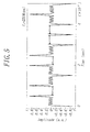
- S/N of the output signal obtained from the ideal SAW matched filter designed on the basis of the group velocity v g is denoted as 0 dB.
- Fig. 6 there is shown a deviation ⁇ V s in the velocity from the group velocity v g in the known SAW matched filter in which the tap distance L is designed in accordance with the phase velocity v s .
- the tap distance L is preferably set to a value within a range from -3 % to +2 % of the ideal value.
- the substrate is formed by the sapphire main body and the thin film of aluminum nitride applied on the main body.
- the sapphire main body may be replaced by a diamond main body
- the thin film of aluminum nitride may be replaced by a piezoelectric zinc oxide thin film.
- the substrate may be composed of a silicon base, a diamond film applied on the silicon base and a piezoelectric thin film applied on the diamond film. It should be noted that the design concept according to the invention may be applied to any type of substrates revealing the dispersity.
- the surface acoustic wave matched filter since the tap distance of the output side electrode is designed not on the basis of the phase velocity, but on the basis of the group velocity, the correlation peak level of the output demodulated signal is improved and S/N of the output demodulated signal is high. Therefore, the output demodulated signal can be processed by a rather simple circuit and a power consumption can be decreased. Due to such merits, the surface acoustic wave matched filter may be particularly advantageously used in a small portable type communication system.
Landscapes
- Physics & Mathematics (AREA)
- Acoustics & Sound (AREA)
- Surface Acoustic Wave Elements And Circuit Networks Thereof (AREA)
Applications Claiming Priority (2)
| Application Number | Priority Date | Filing Date | Title |
|---|---|---|---|
| JP20164898A JP3291248B2 (ja) | 1998-07-16 | 1998-07-16 | 弾性表面波マッチトフィルタ |
| JP20164898 | 1998-07-16 |
Publications (2)
| Publication Number | Publication Date |
|---|---|
| EP0973257A2 true EP0973257A2 (fr) | 2000-01-19 |
| EP0973257A3 EP0973257A3 (fr) | 2001-01-24 |
Family
ID=16444578
Family Applications (1)
| Application Number | Title | Priority Date | Filing Date |
|---|---|---|---|
| EP19990305596 Withdrawn EP0973257A3 (fr) | 1998-07-16 | 1999-07-14 | Filtre adapté aux ondes acoustiques de surface |
Country Status (3)
| Country | Link |
|---|---|
| US (1) | US6275123B1 (fr) |
| EP (1) | EP0973257A3 (fr) |
| JP (1) | JP3291248B2 (fr) |
Cited By (1)
| Publication number | Priority date | Publication date | Assignee | Title |
|---|---|---|---|---|
| EP1211632A3 (fr) * | 2000-12-01 | 2003-09-17 | Fujitsu Limited | Ecran tactile |
Families Citing this family (8)
| Publication number | Priority date | Publication date | Assignee | Title |
|---|---|---|---|---|
| JP2000174663A (ja) * | 1998-12-09 | 2000-06-23 | Kazuo Tsubouchi | 符号分割多重通信方式 |
| US6659161B1 (en) | 2000-10-13 | 2003-12-09 | Chien-Min Sung | Molding process for making diamond tools |
| US7132309B2 (en) | 2003-04-22 | 2006-11-07 | Chien-Min Sung | Semiconductor-on-diamond devices and methods of forming |
| US6814130B2 (en) * | 2000-10-13 | 2004-11-09 | Chien-Min Sung | Methods of making diamond tools using reverse casting of chemical vapor deposition |
| JP4502553B2 (ja) * | 2000-12-05 | 2010-07-14 | 日本碍子株式会社 | 弾性表面波デバイス用基板の製造方法 |
| US20050135759A1 (en) * | 2003-12-22 | 2005-06-23 | Xingwu Wang | Optical fiber assembly |
| EP2123622B1 (fr) | 2007-02-23 | 2011-05-18 | Mitsui Chemicals, Inc. | Procédé de production d'un composé aromatique alkylé |
| US7846767B1 (en) | 2007-09-06 | 2010-12-07 | Chien-Min Sung | Semiconductor-on-diamond devices and associated methods |
Citations (1)
| Publication number | Priority date | Publication date | Assignee | Title |
|---|---|---|---|---|
| JPH05235629A (ja) * | 1992-02-19 | 1993-09-10 | Mitsubishi Electric Corp | マイクロストリップアンテナ |
Family Cites Families (9)
| Publication number | Priority date | Publication date | Assignee | Title |
|---|---|---|---|---|
| GB2181918B (en) | 1982-03-11 | 1987-11-18 | Nobuo Mikoshiba | Surface acoustic wave device |
| US4506239A (en) * | 1982-10-25 | 1985-03-19 | Motorola, Inc. | Compound surface acoustic wave matched filters |
| JPH05235691A (ja) * | 1992-02-24 | 1993-09-10 | Clarion Co Ltd | 弾性表面波装置 |
| EP0569007A2 (fr) * | 1992-05-08 | 1993-11-10 | Canon Kabushiki Kaisha | Dispositif à ondes acoustiques de surface, démodulateur et système de communication utilisant ce dispositif à ondes de surface |
| GB2303265B (en) * | 1995-07-10 | 1998-07-08 | Matsushita Electric Industrial Co Ltd | Spread spectrum communication apparatus,and demodulator,surface acoustic wave element and surface acoustic wave parts for spread spectrum communication |
| JPH0998061A (ja) * | 1995-07-24 | 1997-04-08 | Canon Inc | Sawマッチドフィルタ及びこれを用いた受信装置及び通信システム |
| JP3712291B2 (ja) * | 1996-03-12 | 2005-11-02 | 和夫 坪内 | 表面弾性波デバイスを用いた無線スイッチ装置 |
| JPH09261121A (ja) * | 1996-03-22 | 1997-10-03 | Kazuo Tsubouchi | 符号分割多重通信装置 |
| JP3338628B2 (ja) | 1997-04-25 | 2002-10-28 | 和夫 坪内 | 弾性表面波マッチトフィルタ |
-
1998
- 1998-07-16 JP JP20164898A patent/JP3291248B2/ja not_active Expired - Fee Related
-
1999
- 1999-07-12 US US09/351,944 patent/US6275123B1/en not_active Expired - Lifetime
- 1999-07-14 EP EP19990305596 patent/EP0973257A3/fr not_active Withdrawn
Patent Citations (1)
| Publication number | Priority date | Publication date | Assignee | Title |
|---|---|---|---|---|
| JPH05235629A (ja) * | 1992-02-19 | 1993-09-10 | Mitsubishi Electric Corp | マイクロストリップアンテナ |
Non-Patent Citations (1)
| Title |
|---|
| PATENT ABSTRACTS OF JAPAN vol. 017, no. 691 (E - 1479) 17 December 1993 (1993-12-17) * |
Cited By (2)
| Publication number | Priority date | Publication date | Assignee | Title |
|---|---|---|---|---|
| EP1211632A3 (fr) * | 2000-12-01 | 2003-09-17 | Fujitsu Limited | Ecran tactile |
| US6762753B2 (en) | 2000-12-01 | 2004-07-13 | Fujitsu Limited | Touch panel device |
Also Published As
| Publication number | Publication date |
|---|---|
| EP0973257A3 (fr) | 2001-01-24 |
| JP2000031784A (ja) | 2000-01-28 |
| US6275123B1 (en) | 2001-08-14 |
| JP3291248B2 (ja) | 2002-06-10 |
Similar Documents
| Publication | Publication Date | Title |
|---|---|---|
| US6587016B2 (en) | Surface acoustic wave filter with angled reflection by piezoelectric substrate reflection edges, duplexer, and communication device | |
| EP0435189B1 (fr) | Dispositif à ondes acoustiques de surface | |
| US7692515B2 (en) | Low-loss electro-acoustic component | |
| US10886893B2 (en) | Reduced-size guided-surface acoustic wave (SAW) devices | |
| US6476691B1 (en) | Surface acoustic wave filter | |
| EP0973257A2 (fr) | Filtre adapté aux ondes acoustiques de surface | |
| KR100339719B1 (ko) | 고주파표면탄성파(saw)장치,그형성방법및이에사용되는랑거사이트기판 | |
| EP1160974B1 (fr) | Système de communication sans fil utilisant des techniques de transducteurs unidirectionnels monophases à ondes acoustiques de surface | |
| WO2022103405A1 (fr) | Agencements de couches piézoélectriques dans des dispositifs à ondes acoustiques et procédés associés | |
| CN112655150A (zh) | 弹性波装置、高频前端电路以及通信装置 | |
| US12255611B2 (en) | Thin-film saw device with multilayer waveguide | |
| EP0602660A2 (fr) | Dispositif à ondes acoustiques de surface et système de communication utilisant ce dispositif | |
| EP0641072B1 (fr) | Dispositif à ondes acoustiques de surface | |
| US6906602B2 (en) | Surface acoustic wave filter utilizing two parallel acoustic channels with one having a narrower bandwidth | |
| EP0569007A2 (fr) | Dispositif à ondes acoustiques de surface, démodulateur et système de communication utilisant ce dispositif à ondes de surface | |
| US20230208391A1 (en) | Acoustic wave device | |
| US7187101B2 (en) | Surface acoustic wave filter | |
| US4393321A (en) | Surface acoustic wave transducer | |
| EP0744830B1 (fr) | Dispositif a ondes acoustiques de surface et procede de production | |
| Kadota et al. | Small and low-loss IF SAW filters using zinc oxide film on quartz substrate | |
| JPH09219632A (ja) | 表面弾性波素子 | |
| US6407650B1 (en) | Surface acoustic wave shaping system | |
| US6268680B1 (en) | Surface acoustic wave transducer | |
| Lever et al. | Surface acoustic wave matched filters for communications systems | |
| JP2006157557A (ja) | 弾性表面波装置 |
Legal Events
| Date | Code | Title | Description |
|---|---|---|---|
| PUAI | Public reference made under article 153(3) epc to a published international application that has entered the european phase |
Free format text: ORIGINAL CODE: 0009012 |
|
| AK | Designated contracting states |
Kind code of ref document: A2 Designated state(s): DE FR GB |
|
| AX | Request for extension of the european patent |
Free format text: AL;LT;LV;MK;RO;SI |
|
| PUAL | Search report despatched |
Free format text: ORIGINAL CODE: 0009013 |
|
| AK | Designated contracting states |
Kind code of ref document: A3 Designated state(s): AT BE CH CY DE DK ES FI FR GB GR IE IT LI LU MC NL PT SE |
|
| AX | Request for extension of the european patent |
Free format text: AL;LT;LV;MK;RO;SI |
|
| RIC1 | Information provided on ipc code assigned before grant |
Free format text: 7H 03H 9/64 A, 7H 04B 1/707 B |
|
| 17P | Request for examination filed |
Effective date: 20010123 |
|
| AKX | Designation fees paid |
Free format text: DE FR GB |
|
| 17Q | First examination report despatched |
Effective date: 20020320 |
|
| STAA | Information on the status of an ep patent application or granted ep patent |
Free format text: STATUS: THE APPLICATION IS DEEMED TO BE WITHDRAWN |
|
| 18D | Application deemed to be withdrawn |
Effective date: 20041130 |