EP0973264B1 - Chipströmedekodierung - Google Patents
Chipströmedekodierung Download PDFInfo
- Publication number
- EP0973264B1 EP0973264B1 EP98305567A EP98305567A EP0973264B1 EP 0973264 B1 EP0973264 B1 EP 0973264B1 EP 98305567 A EP98305567 A EP 98305567A EP 98305567 A EP98305567 A EP 98305567A EP 0973264 B1 EP0973264 B1 EP 0973264B1
- Authority
- EP
- European Patent Office
- Prior art keywords
- chip
- oversamples
- dec
- clock
- signal
- Prior art date
- Legal status (The legal status is an assumption and is not a legal conclusion. Google has not performed a legal analysis and makes no representation as to the accuracy of the status listed.)
- Expired - Lifetime
Links
- 238000000034 method Methods 0.000 claims description 22
- 238000005070 sampling Methods 0.000 claims description 6
- 230000004044 response Effects 0.000 claims description 2
- 239000000284 extract Substances 0.000 description 13
- 238000004891 communication Methods 0.000 description 5
- 230000008859 change Effects 0.000 description 4
- 238000010586 diagram Methods 0.000 description 4
- 230000003111 delayed effect Effects 0.000 description 3
- 230000009471 action Effects 0.000 description 2
- 238000013459 approach Methods 0.000 description 2
- 238000004519 manufacturing process Methods 0.000 description 2
- 230000008569 process Effects 0.000 description 2
- 230000001360 synchronised effect Effects 0.000 description 2
- 239000000872 buffer Substances 0.000 description 1
- 230000003247 decreasing effect Effects 0.000 description 1
- 230000001934 delay Effects 0.000 description 1
- 238000011161 development Methods 0.000 description 1
- 230000018109 developmental process Effects 0.000 description 1
- 238000013507 mapping Methods 0.000 description 1
- 238000012986 modification Methods 0.000 description 1
- 230000004048 modification Effects 0.000 description 1
- 230000000630 rising effect Effects 0.000 description 1
- 238000001228 spectrum Methods 0.000 description 1
Images


Classifications
-
- H—ELECTRICITY
- H04—ELECTRIC COMMUNICATION TECHNIQUE
- H04L—TRANSMISSION OF DIGITAL INFORMATION, e.g. TELEGRAPHIC COMMUNICATION
- H04L7/00—Arrangements for synchronising receiver with transmitter
- H04L7/02—Speed or phase control by the received code signals, the signals containing no special synchronisation information
- H04L7/033—Speed or phase control by the received code signals, the signals containing no special synchronisation information using the transitions of the received signal to control the phase of the synchronising-signal-generating means, e.g. using a phase-locked loop
- H04L7/0334—Processing of samples having at least three levels, e.g. soft decisions
-
- H—ELECTRICITY
- H04—ELECTRIC COMMUNICATION TECHNIQUE
- H04B—TRANSMISSION
- H04B1/00—Details of transmission systems, not covered by a single one of groups H04B3/00 - H04B13/00; Details of transmission systems not characterised by the medium used for transmission
- H04B1/69—Spread spectrum techniques
- H04B1/707—Spread spectrum techniques using direct sequence modulation
Definitions
- This invention is concerned with streams of data which have been encoded into a chip stream so that a chip rate and phase of the chip stream can be derived from the encoded data, and in particular the invention relates to a method of and an apparatus for decoding such chip streams.
- a traditional digital PLL oversamples the received chip stream using a clock having a frequency which is an integer multiple of the transmitted chip rate.
- the chip rate is increased (to provide faster communication) and/or as the multiplier of the oversampling clock is increased (to provide better the operation of the PLL), the frequency of the oversampling clock can become unmanageably high.
- an analogue, rather than digital, PLL might be used.
- such an analogue PLL would either need to be integrated with the receiver (or transceiver) section, occupy a special analogue support IC, or be integrated into a mixed signal controller. All of these options are more costly than integrating the PLL into the digital controller.
- United States patent US-A-5077753 relates to a spread spectrum radio communication system that correlates a demodulated signal with a pseudorandom chipping sequence and extracts clock and data signals.
- the chipping sequence is normally selected from a set of codes including an eleven bit Basker code.
- the present invention is concerned with the above problems and in particular with recovering data and timing information in such a way that it can be performed in a digital controller without the need for an oversampling clock, i.e. a clock having a clock rate which is many times faster than the chip rate.
- a method of decoding a stream of data which has been encoded into a chip stream so that a chip rate and phase of the chip stream can be derived from the encoded data comprising decoding steps of: generating a clock signal (clk) having a clock rate which is approximately equal to the chip rate or an integer multiple thereof; characterised in that the method further comprises: passing the chip stream along a multi-stage delay line having a delay per stage that is less than the period of the clock signal; for each clock cycle, sampling data of the chip stream at a plurality of the stages of the delay line to produce a set of oversamples (oversamples, Q0-Q6) for each chip period; for each clock cycle, producing an estimate (edgepos) of a position in a respective set of the oversamples of a chip edge in the chip stream; for at least some of the clock cycles, selecting at least one of the oversamples (dec_chip(0), dec_chip
- the PLL operates to adjust the clock frequency, and therefore a variable frequency oscillator is required.
- a PLL action may be obtained in the present invention by adjusting the estimate of the position in the oversamples of the chip edge, thus obviating the need for a variable frequency oscillator.
- the clock rate is preferably fixed.
- each selected oversample preferably has a predetermined position with respect to the estimated chip edge position.
- the method preferably further includes the calibration steps of: passing a signal having a known period (for example the above-mentioned clock signal) into the delay line; sampling data of the known period signal at a plurality of stages of the delay line to produce a set of calibration oversamples; estimating from the sampled data an indication of the delay per stage of the delay line; and storing the delay per stage indication.
- the calibration steps are preferably performed intermittently and while the decoding steps are not being performed.
- the calibration steps may be performed at power-on, when the apparatus is transmitting, and when the communications link is being turned around.
- the step of selecting at least one of the oversamples preferably comprises the steps of: for each clock cycle, making a first selection of some of the oversamples in dependence upon the stored delay indication; for at least some of the clock cycles, making a second selection, from the first selection of the oversamples, of said at least one of the oversamples having a predetermined position with respect to the estimated chip edge position.
- a PLL action may be obtained in the present invention by adjusting the estimate of the position in the oversamples of the chip edge.
- the step of producing the chip edge position estimate preferably comprises the steps of: storing a chip edge position estimate; for at least some of the clock cycles, detecting any deviation of the chip edge position from the stored chip edge position estimate; and in response to such a detected deviation, adjusting the stored chip edge position estimate.
- the stored chip edge position estimate may be limited to having a predetermined range of values. In this case, special steps may be taken if the chip edge position estimate is about to be adjusted so that it is outside the range.
- the value of the stored chip edge position estimate needs to be adjusted past one end of its range, it is instead adjusted to the other end of its range and none of the oversamples is selected for output; and if, for a clock cycle, the value of the stored chip edge position estimate needs to be adjusted past said other end of its range, it is instead adjusted to said one end of its range and two of the oversamples are selected for output.
- an apparatus for decoding a stream of data which has been encoded into a chip stream so that a chip rate and phase of the chip stream can be derived from the encoded data comprising: a clock (10) for generating a clock signal (clk) having a clock rate which is approximately equal to the chip rate or an integer multiple thereof characterised in that the apparatus further comprises; a multi-stage delay line (14, 26(0)-(6)) for receiving the chip stream having a delay per stage that is less than the period of the clock signal; means clocked by the clock signal for sampling data of the chip stream at each stage of the delay line to produce a set of oversamples ( oversamples, Q0-Q6) for each chip period; means (20,22) clocked by the clock signal for producing an estimate (edgepos) of a position in a respective set of the oversamples of a chip edge in the chip stream; means (20,22,24) responsive to the clock signal for selecting, for
- This apparatus is preferably operable to perform any one or more of the preferred features of the method of the first aspect of the invention.
- the apparatus has two modes of operation: “decoding” and “calibration”.
- the calibration mode is employed repeatedly when the apparatus is not receiving, for example at power-on, when the apparatus is transmitting, and when the communications link is being turned around.
- a square-wave clock signal clk from a clock generator 10 (or some other signal of known period) is passed by a switch 12, under control of a calibration control circuit 16, as a signal dl_input to a multi-stage sampled delay line circuit 14.
- the clk signal is also supplied as a clock input to the delay line circuit 14 .
- Each stage of the delay line circuit 14 provides a delay which is shorter than the period of the clk signal, which can vary as between one circuit and another due to manufacturing tolerances, and which can drift with time, voltage and temperature.
- Each stage of the delay line circuit 14 is tapped to provide a respective element of an oversamples signal.
- the oversamples signal is fed to the calibration control circuit 16, which determines the number of stages of the delay line circuit 14 which together produce a delay generally equal to the period of the clk signal, and this number is stored as a signal ffs_per_cycle .
- the decoding mode of the apparatus is employed when the apparatus is receiving.
- the apparatus receives a chip stream signal rxchip which has a chip rate approximately equal to the frequency of the clk signal.
- the chip stream signal rxchip is passed by the switch 12, under control of the calibration control circuit 16, as the dl_input signal to the delay line circuit 14.
- the delay line circuit 14 produces, with each cycle of the clk signal, an oversamples signal having a number of samples equal to the number of stages in the delay line circuit 14, and the oversamples signal is passed to a phase pick circuit 18, which also receives the previously calculated ffs_per_cycle signal from the calibration control circuit 16.
- the phase pick circuit 18 selects a predetermined number of samples of the oversamples signal spread as regularly as possible over the first ffs_per_cycle samples, beginning with the least delayed sample.
- the selected samples are passed as a signal picked_samples to an edge extract circuit 20, which stores that signal as current_picked_samples and also stores the immediately preceding signal as previous_picked_samples.
- the edge extract circuit 20 operates in cooperation with an edge position circuit 22 as a phase-locked loop.
- the edge position circuit 22 maintains a signal edgepos which is an estimate of the position within current_picked_samples and previous_picked_samples of a chip edge of the chip stream, and the edgepos signal is supplied to the edge extract circuit 20.
- the edge extract circuit 20 generates an estimate of whether the edge of the incoming chip occurs earlier or later than expected, as a function of current_picked_samples, previous_picked_samples and edgepos, and produces a corresponding up_or_down signal which is supplied to the edge position circuit 22.
- the edge position circuit 22 modifies the value of the edgepos signal in dependence upon the up_or_down signal.
- the edge extract circuit 20 selects two of the samples from the set current_picked_samples and previous_picked_samples and supplies them as dec_chip(0), dec_chip(1) to a rebuild circuit 24, the two selected samples dec_chip(0), dec_chip(1) being equally spaced by a predetermined amount to either side of the edgepos position within current_picked_samples and previous_picked_samples.
- the edge position circuit 22 produces a signal n_dec_chips indicating whether or not each of the selected samples dec_chip(0), dec_chip_(1) is to be used in decoding the chip stream, and supplies the signal n_dec_chips to the rebuild circuit 24. Furthermore, with each cycle of the clk signal, the rebuild circuit 24 selects none, one, the other, or both of the samples dec_chip(0), dec_chip(1) in dependence upon the value of n_dec_chips and includes it/them in an output signal decoded_stream, or serial-to-parallel converts the bits to produce a parallel output signal.
- the chip rate of the rxchip signal were exactly equal to the frequency of the clk signal (and if the delay of each stage in the delay line 14 never varied), then in one reception session the value of the edgepos signal would remain constant, and with each cycle of the clk signal a sample at a constant position in the set current_picked_samples and previous_picked_samples would be selected for the output.
- the clk signal is not synchronised with the rxchip signal.
- the apparatus modifies the value of the edgepos signal so that, if the frequency of the clk signal is slightly higher than the chip rate of the rxchip signal, the estimated position of the chip edge as defined by the edgepos signal moves in one direction through the set current_picked_samples and previous_picked_samples, and if the frequency of the clk signal is slightly lower than the chip rate of the rxchip signal, the estimated position of the chip edge as defined by the edgepos signal moves in the opposite direction through the set current_picked_samples and previous_picked_samples.
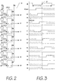
- the dl_input signal is fed to the delay line circuit 14 formed by a series of gates 26(0)-(6), typically non-inverting buffers. Only seven gates 26(0)-(6) are shown in Figure 2 for simplicity; in practice more would probably be provided. Taps are taken from the outputs of the gates 26(0)-(6) to provide signals D0-D6 respectively, which are supplied as the data inputs to a series of flip-flops 28(0)-(6) which are clocked by the clk signal. The outputs Q0-Q6 from the flip-flops 28(0)-(6) form the oversamples signal.
- the n th flip-flop 26 ( n-1 ) will contain a sample of rxchip at time t - n.T g , where t is the current time.
- the delay line circuit 14 must have sufficient stages to provide a sufficient number of samples under slowest gate conditions and to cover a whole chip period under fastest gate conditions.
- FIG. 3 is a timing diagram for the delay line circuit 14 when operating in the decoding mode.
- the clk signal of period T c is shown in the top section of the drawing.
- the flip-flops 28(0)-(6) latch on the rising edge 30 of the clk signal.
- the next section of Figure 3 shows in continuous line a portion of the dl_input signal.
- the remaining sections of Figure 3 show in pairs the input signals D0-D6 to, and corresponding output signals Q0-Q6 from, the flip-flops 28(0)-(6).
- each signal D n from a particular gate 26( n ) is delayed by T g with respect to the signal D( n -1) from the preceding gate 26( n -1) in the delay line circuit 14.
- an oversamples signal of (Q0,..., Q6) (1,1,1,0,0,0,0) is produced.
- the selection of the samples in oversamples for various values of ffs_per_cycle may be as given in the following table. Mapping of oversamples onto picked _samples for various ffs_per_cycle , where number of samples in picked _samples equals six.
- phase pick circuit 18 may be implemented by an array of logic gates or in other ways.
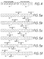
- the selected samples in picked_samples are passed with each cycle of the clk signal to the edge extract circuit 20, which stores the received signal as current_picked_samples, in a register 32 as shown in Figure 4, and also stores the immediately preceding signal as previous_picked_samples (containing samples pP0,..., pP5) in a register 34.
- the edge extract circuit 20 receives an edgepos signal from the edge position circuit 22.
- the edgepos signal can take the same number of values as the number of samples in picked_samples, i.e. six in the example given such as 0 ⁇ edgepos ⁇ 5.
- the edge extract circuit 20 outputs two of the samples dec_chip(0), dec_chip(1) which are equally spaced by a predetermined amount to either side of the edgepos position.
- edgepos edgepos points to dec_chip (0) dec_chip (1) between and 0 P2 P3 P5 P0 1 P3 P4 pP0 P1 2 P4 P5 pP1 P2 3 P5 pP0 pP2 P3 4 pP0 pP1 pP3 P4 5 pP1 pP2 pP4 P5
- Figures 5a-f show examples of the samples P0-P5,pP0-pP5 of the chip stream with edgepos being correctly aligned with a chip edge in the chipstream.
- the edge extract circuit 20 determines whether edgepos appears to have drifted from such a chip edge. For example, if the two samples to the left and the two samples to the right of edgepos are (reading from left to right) 1,0,0,0 or 0,1,1,1, then edgepos needs to be increased, and this is indicated to the edge position circuit 22 by the up_or_down signal.
- edgepos needs to be decreased, and this is indicated to the edge position circuit 22 by the up_or_down signal. If, however, the two samples to the left and the right of edgepos are 1,1,0,0 or 0,0,1,1, this indicates that edgepos is correctly positioned. If the two samples to the left and the right of edgepos are 0,0,0,0, it is taken that it is not possible to determine whether edgepos is correctly positioned. If the two samples to the left and the right of edgepos are 1,1,1,1, the third sample to the left is tested.
- edgepos is initially given an arbitrary value such as zero.
- edgepos is initially given an arbitrary value such as zero.
- four samples are normally used to assess the correctness of edgepos, but other numbers of samples, for example six samples could normally be used.
- the edge extract circuit 20 may be implemented by an array of logic gates or in other ways.
- the edge position circuit 22 receives the up_or_down signal and produces the edgepos signal and the n_dec_chips signal. In determining whether to change the edgepos signal, the edge position circuit 22 may be arranged to respond, if appropriate, to each up_or_down signal independently for each cycle of the clk signal, or it may be arranged, for example, to average the up_or_down signals for two or more successive cycles of the clk signal. In most cases, the n_dec_chips signal produced by the edge position circuit 22 indicates that only one of the samples dec_chip(0), dec_chip(1) output by the edge extract circuit 20 is to be used by the rebuild circuit 24, for example dec_chip(0).
- edgepos does not change, or it is incremented or decremented by one between its minimum and maximum values (0 and 5 in the example), the value of n_dec_chips does not change.
- n_dec_chips does not change.
- n_dec_chips is set so that neither dec_chip(0) nor dec_chip(1) is used.
- edgepos is set to 5, and the dec_chip(0) sample is used. Accordingly, with the values of the samples shown in Figures 6a-c, the output obtained is:
- edge position circuit 22 and rebuild circuit 24 may be implemented by an array of logic gates or in other ways.
- the edge extract circuit uses current_picked_samples and previous_picked_samples.
- the delay-line circuit 14 could include twice as many stages, and the phase pick circuit 18 could pick twice as many samples spread over the first 2 x ffs_per_cycle samples, so that, in the example given, the number of samples in picked_samples would be twelve.
Landscapes
- Engineering & Computer Science (AREA)
- Computer Networks & Wireless Communication (AREA)
- Signal Processing (AREA)
- Synchronisation In Digital Transmission Systems (AREA)
- Stabilization Of Oscillater, Synchronisation, Frequency Synthesizers (AREA)
Claims (11)
- Ein Verfahren zum Decodieren eines Datenstroms, der in einen Chipstrom codiert wurde, so dass eine Chiprate und eine Phase des Chipstroms aus den codierten Daten abgeleitet werden können, wobei das Verfahren folgende Decodierschritte aufweist:Erzeugen eines Taktsignals (clk), das eine Taktrate aufweist, die näherungsweise gleich der Chiprate oder ein ganzzahliges Vielfaches derselben ist; dadurch gekennzeichnet, dass das Verfahren ferner folgende Schritte aufweist:Leiten des Chipstroms entlag einer mehrstufigen Verzögerungsleitung (14, 26(0)-(6)), die eine Verzögerung pro Stufe aufweist, die geringer als die Periode des Taktsignals ist;Abtasten von Daten des Chipstroms für jeden Taktzyklus bei einer Mehrzahl der Stufen der Verzögerungsleitung, um einen Satz von Überabtastungen (Überabtastungen, Q0-Q6) für jede Chipperiode zu erzeugen;Erzeugen eines Schätzwerts (Kantenpos) einer Position einer Chipkante in dem Chipstrom in einem jeweiligen Satz der Überabtastungen für jeden Taktzyklus;Auswählen zumindest einer der Überabtastungen (dec_chip (0), dec_chip (1)), die eine Position innerhalb eines eingegrenzten Bereichs mit Bezug auf die geschätzte Chipkantenposition aufweist, für zumindest einige der Taktzyklen; undAusgeben der ausgewählten Überabtastungen.
- Ein Verfahren gemäß Anspruch 1, bei dem die Taktrate fest ist.
- Ein Verfahren gemäß Anspruch 1 oder 2, bei dem die ausgewählte Überabtastung eine vorbestimmte Position mit Bezug auf die geschätzte Chipkantenposition aufweist.
- Ein Verfahren gemäß einem der vorhergehenden Ansprüche, bei dem die Verzögerung pro Stufe (T g ) der Verzögerungsleitung unstabilisiert ist.
- Ein Verfahren gemäß einem der vorhergehenden Ansprüche, das ferner Kalibrierungsschritte umfasst, die folgende Schritte aufweisen:Leiten eines Signals (clk), das eine bekannte Periode aufweist, in die Verzögerungsleitung;Abtasten von Daten des Signals mit bekannter Periode an einer Mehrzahl von Stufen der Verzögerungsleitung, um einen Satz von Kalibrierungsüberabtastungen (Überabtastungen, Q0-Q6) zu erzeugen;Schätzen einer Angabe (ffs_pro_Zyklus) der Verzögerung pro Stufe der Verzögerungsleitung aus den abgetasteten Daten; undSpeichern der Angabe einer Verzögerung pro Stufe.
- Ein Verfahren gemäß Anspruch 5, bei dem das Signal mit bekannter Periode das Taktsignal (clk) ist.
- Ein Verfahren gemäß Anspruch 5 oder 6, bei dem die Kalibrierungsschritte intermittierend durchgeführt werden, während die Decodierschritte nicht durchgeführt werden.
- Ein Verfahren gemäß einem der Ansprüche 5 bis 7, bei dem bei den Decodierschritten der Schritt des Auswählens zumindest einer der Überabtastungen (dec_chip(0), dec_chip (1)) folgende Schritte aufweist:Vornehmen einer ersten Auswahl einiger der Überabtastungen (ausgewählte_Abtastwerte) für jeden Taktzyklus in Abhängigkeit von der gespeicherten Verzögerungsangabe (ffs_pro_Zyklus);Vornehmen einer zweiten Auswahl von zumindest einer der Überabtastungen (dec_chip (0), dec_chip(1)), die eine vorbestimmte Position mit Bezug auf die geschätzte Chipkantenposition aufweist, aus der ersten Auswahl der Überabtastungen für zumindest einige der Taktzyklen.
- Ein Verfahren gemäß einem der vorhergehenden Ansprüche, bei dem bei den Decodierschritten der Schritt des Erzeugens des Chipkantenpositionsschätzwerts (Kantenpos) folgende Schritte aufweist:Speichern eines Chipkantenpositionsschätzwerts;Erfassen irgendeiner Abweichung der Chipkantenposition von dem gespeicherten Chipkantenpositionsschätzwert für zumindest einige der Taktzyklen; undEinstellen des gespeicherten Chipkantenpositionsschätzwerts ansprechend auf eine derartige erfasste Abweichung.
- Ein Verfahren gemäß Anspruch 9, bei dem:der gespeicherte Chipkantenpositionsschätzwert einen vorbestimmten Bereich von Werten aufweist;falls für einen Taktzyklus der Wert des gespeicherten Chipkantenpositionsschätzwerts über ein Ende des Bereichs desselben hinaus eingestellt werden muss, derselbe anstelle dessen auf das andere Ende des Bereichs desselben eingestellt wird und keine der Überabtastungen (dec_chip (0), dec_chip (1)) für eine Ausgabe ausgewählt wird; undfalls für einen Taktzyklus der Wert des gespeicherten Chipkantenpositionsschätzwert über das andere Ende des Bereichs desselben hinaus eingestellt werden muss, derselbe anstelle dessen auf das eine Ende des Bereichs desselben eingestellt wird und zwei der Überabtastungen (dec_chip (0), dec_chip (1)) für eine Ausgabe ausgewählt werden.
- Eine Vorrichtung zum Decodieren eines Datenstroms, der in einen Chipstrom codiert wurde, so dass eine Chiprate und eine Phase des Chipstroms aus den codierten Daten abgeleitet werden können, wobei die Vorrichtung folgende Merkmale aufweist:einen Takt (10) zum Erzeugen eines Taktsignals (clk), das eine Taktrate aufweist, die näherungsweise gleich der Chiprate oder ein ganzzahliges Vielfaches derselben ist, dadurch gekennzeichnet, dass die Vorrichtung ferner folgende Merkmale aufweist:eine mehrstufige Verzögerungsleitung (14, 26(0)-(6)) zum Empfangen des Chipstroms, die eine Verzögerung pro Stufe aufweist, die geringer als die Periode des Taktsignals ist;eine Einrichtung (14, 28 (0) - (6)), die durch das Taktsignal getaktet ist, zum Abtasten von Daten des Chipstroms bei jeder Stufe der Verzögerungsleitung, um einen Satz von Überabtastungen (Überabtastungen, Q0-Q6) für jede Chipperiode zu erzeugen;eine Einrichtung (20, 22) die durch das Taktsignal getaktet ist, zum Erzeugen eines Schätzwerts (Kantenpos) einer Position einer Chipkante in dem Chipstrom in einem jeweiligen Satz der Überabtastungen;eine Einrichtung (20, 22, 24), die auf das Taktsignal anspricht, zum Auswählen zumindest einer der Überabtastungen (dec_chip (0), dec_chip (1)), die eine Position innerhalb eines eingegrenzten Bereichs mit Bezug auf die geschätzte Chipkantenposition aufweist, für zumindest einige der Taktzyklen; undeine Einrichtung (24) zum Ausgeben der ausgewählten Überabtastungen.
Priority Applications (4)
| Application Number | Priority Date | Filing Date | Title |
|---|---|---|---|
| EP98305567A EP0973264B1 (de) | 1998-07-13 | 1998-07-13 | Chipströmedekodierung |
| DE69835874T DE69835874T2 (de) | 1998-07-13 | 1998-07-13 | Chipströmedekodierung |
| JP19897999A JP2000059350A (ja) | 1998-07-13 | 1999-07-13 | チップ・ストリ―ムの復号化 |
| US09/352,826 US6438155B1 (en) | 1998-07-13 | 1999-07-13 | Decoding chip streams |
Applications Claiming Priority (1)
| Application Number | Priority Date | Filing Date | Title |
|---|---|---|---|
| EP98305567A EP0973264B1 (de) | 1998-07-13 | 1998-07-13 | Chipströmedekodierung |
Publications (2)
| Publication Number | Publication Date |
|---|---|
| EP0973264A1 EP0973264A1 (de) | 2000-01-19 |
| EP0973264B1 true EP0973264B1 (de) | 2006-09-13 |
Family
ID=8234933
Family Applications (1)
| Application Number | Title | Priority Date | Filing Date |
|---|---|---|---|
| EP98305567A Expired - Lifetime EP0973264B1 (de) | 1998-07-13 | 1998-07-13 | Chipströmedekodierung |
Country Status (4)
| Country | Link |
|---|---|
| US (1) | US6438155B1 (de) |
| EP (1) | EP0973264B1 (de) |
| JP (1) | JP2000059350A (de) |
| DE (1) | DE69835874T2 (de) |
Families Citing this family (6)
| Publication number | Priority date | Publication date | Assignee | Title |
|---|---|---|---|---|
| US6950484B1 (en) * | 2000-05-12 | 2005-09-27 | Cypress Semiconductor Corp. | Linearized digital phase-locked loop method |
| GB2396275B (en) * | 2002-12-09 | 2006-03-15 | Ipwireless Inc | Support of plural chip rates in a CDMA system |
| US7826581B1 (en) | 2004-10-05 | 2010-11-02 | Cypress Semiconductor Corporation | Linearized digital phase-locked loop method for maintaining end of packet time linearity |
| US7298299B1 (en) * | 2004-10-21 | 2007-11-20 | Altera Corporation | Efficient data recovery algorithm for serial data |
| JP4904596B2 (ja) | 2004-12-03 | 2012-03-28 | エスティー‐エリクソン、ソシエテ、アノニム | ディジタル遅延線中のタップ位置の管理 |
| CA2682103A1 (en) | 2009-10-27 | 2010-01-05 | Avalon Microelectronics, Inc. | Method and apparatus for deskewing data transmissions |
Family Cites Families (8)
| Publication number | Priority date | Publication date | Assignee | Title |
|---|---|---|---|---|
| US4930139A (en) * | 1989-05-31 | 1990-05-29 | O'neill Communications, Inc. | Spread spectrum communication system |
| US5093841A (en) * | 1990-01-30 | 1992-03-03 | Nynex Corporation | Clock acquisition in a spread spectrum system |
| US5077753A (en) * | 1990-04-09 | 1991-12-31 | Proxim, Inc. | Radio communication system using spread spectrum techniques |
| US5319735A (en) * | 1991-12-17 | 1994-06-07 | Bolt Beranek And Newman Inc. | Embedded signalling |
| US5920555A (en) * | 1994-07-28 | 1999-07-06 | Roke Manor Research Limited | Pilot assisted direct sequence spread spectrum synchronization apparatus |
| US5692006A (en) * | 1995-07-31 | 1997-11-25 | Qualcomm Incorporated | Adaptive despreader |
| US6356555B1 (en) * | 1995-08-25 | 2002-03-12 | Terayon Communications Systems, Inc. | Apparatus and method for digital data transmission using orthogonal codes |
| US6014405A (en) * | 1997-10-24 | 2000-01-11 | Golden Bridge Technology, Inc. | Spread spectrum multipath receiver without a tracking loop |
-
1998
- 1998-07-13 DE DE69835874T patent/DE69835874T2/de not_active Expired - Lifetime
- 1998-07-13 EP EP98305567A patent/EP0973264B1/de not_active Expired - Lifetime
-
1999
- 1999-07-13 JP JP19897999A patent/JP2000059350A/ja active Pending
- 1999-07-13 US US09/352,826 patent/US6438155B1/en not_active Expired - Fee Related
Also Published As
| Publication number | Publication date |
|---|---|
| JP2000059350A (ja) | 2000-02-25 |
| US6438155B1 (en) | 2002-08-20 |
| DE69835874D1 (de) | 2006-10-26 |
| EP0973264A1 (de) | 2000-01-19 |
| DE69835874T2 (de) | 2007-04-12 |
Similar Documents
| Publication | Publication Date | Title |
|---|---|---|
| US7577226B2 (en) | Clock recovery circuitry | |
| EP0688103B1 (de) | Einrichtung zum Ableiten eines Taktsignals | |
| US4506372A (en) | Method and apparatus for recognizing in a receiver the start of a telegram signal consisting of a bit impulse sequence | |
| EP0378417A2 (de) | Kodedivisionsmultiplexsystem | |
| EP0651926B1 (de) | Verfahren und anordnung fur die ubertragung, den empfang, die kodierung und dekodierung punktierter faltungskoden | |
| US4964138A (en) | Differential correlator for spread spectrum communication system | |
| EP0124319B1 (de) | Funktelefone | |
| EP0317159B1 (de) | Taktwiedergewinnungsanordnung | |
| EP0425302B1 (de) | Digitaler Phasenregelschleifendekoder, insbesondere für Manchester Kode | |
| EP0383557B1 (de) | Netzwerktakt-Synchronisation | |
| CA2017394C (en) | Data alignment method and apparatus | |
| US9118392B2 (en) | Isolated serializer-deserializer | |
| JPH08163117A (ja) | ビット位相同期回路 | |
| US8259886B2 (en) | Communication apparatus | |
| US5889820A (en) | SPDIF-AES/EBU digital audio data recovery | |
| EP1016233A1 (de) | Kreuzschienenschaltung mit konstanter phase | |
| EP0973264B1 (de) | Chipströmedekodierung | |
| US5168511A (en) | Manchester data recorder with synchronously adjustable clock | |
| US6002731A (en) | Received-data bit synchronization circuit | |
| US5321727A (en) | Signal phasing arrangement in a system for doubling the digital channel | |
| US20010053188A1 (en) | Transmitting circuit and method thereof, receiving circuit and method thereof, and data communication apparatus | |
| US6476738B1 (en) | Block interleave circuit | |
| EP0448045B1 (de) | System zur Unterdrückung der durch differentielle Kodierung verursachten Fehlerverbreitung | |
| JPH06507769A (ja) | クロック同期方法および回路 | |
| US6160822A (en) | ATM cell synchronization circuit |
Legal Events
| Date | Code | Title | Description |
|---|---|---|---|
| PUAI | Public reference made under article 153(3) epc to a published international application that has entered the european phase |
Free format text: ORIGINAL CODE: 0009012 |
|
| AK | Designated contracting states |
Kind code of ref document: A1 Designated state(s): DE FR GB |
|
| AX | Request for extension of the european patent |
Free format text: AL;LT;LV;MK;RO;SI |
|
| 17P | Request for examination filed |
Effective date: 20000525 |
|
| AKX | Designation fees paid |
Free format text: DE FR GB |
|
| RAP1 | Party data changed (applicant data changed or rights of an application transferred) |
Owner name: HEWLETT-PACKARD COMPANY, A DELAWARE CORPORATION |
|
| 17Q | First examination report despatched |
Effective date: 20050614 |
|
| GRAP | Despatch of communication of intention to grant a patent |
Free format text: ORIGINAL CODE: EPIDOSNIGR1 |
|
| GRAS | Grant fee paid |
Free format text: ORIGINAL CODE: EPIDOSNIGR3 |
|
| GRAA | (expected) grant |
Free format text: ORIGINAL CODE: 0009210 |
|
| AK | Designated contracting states |
Kind code of ref document: B1 Designated state(s): DE FR GB |
|
| REG | Reference to a national code |
Ref country code: GB Ref legal event code: FG4D |
|
| REF | Corresponds to: |
Ref document number: 69835874 Country of ref document: DE Date of ref document: 20061026 Kind code of ref document: P |
|
| EN | Fr: translation not filed | ||
| PLBE | No opposition filed within time limit |
Free format text: ORIGINAL CODE: 0009261 |
|
| STAA | Information on the status of an ep patent application or granted ep patent |
Free format text: STATUS: NO OPPOSITION FILED WITHIN TIME LIMIT |
|
| 26N | No opposition filed |
Effective date: 20070614 |
|
| PG25 | Lapsed in a contracting state [announced via postgrant information from national office to epo] |
Ref country code: FR Free format text: LAPSE BECAUSE OF FAILURE TO SUBMIT A TRANSLATION OF THE DESCRIPTION OR TO PAY THE FEE WITHIN THE PRESCRIBED TIME-LIMIT Effective date: 20070518 |
|
| PG25 | Lapsed in a contracting state [announced via postgrant information from national office to epo] |
Ref country code: FR Free format text: LAPSE BECAUSE OF FAILURE TO SUBMIT A TRANSLATION OF THE DESCRIPTION OR TO PAY THE FEE WITHIN THE PRESCRIBED TIME-LIMIT Effective date: 20060913 |
|
| REG | Reference to a national code |
Ref country code: GB Ref legal event code: 732E Free format text: REGISTERED BETWEEN 20120329 AND 20120404 |
|
| PGFP | Annual fee paid to national office [announced via postgrant information from national office to epo] |
Ref country code: GB Payment date: 20130626 Year of fee payment: 16 |
|
| PGFP | Annual fee paid to national office [announced via postgrant information from national office to epo] |
Ref country code: DE Payment date: 20130621 Year of fee payment: 16 |
|
| REG | Reference to a national code |
Ref country code: DE Ref legal event code: R119 Ref document number: 69835874 Country of ref document: DE |
|
| GBPC | Gb: european patent ceased through non-payment of renewal fee |
Effective date: 20140713 |
|
| PG25 | Lapsed in a contracting state [announced via postgrant information from national office to epo] |
Ref country code: DE Free format text: LAPSE BECAUSE OF NON-PAYMENT OF DUE FEES Effective date: 20150203 |
|
| REG | Reference to a national code |
Ref country code: DE Ref legal event code: R119 Ref document number: 69835874 Country of ref document: DE Effective date: 20150203 |
|
| PG25 | Lapsed in a contracting state [announced via postgrant information from national office to epo] |
Ref country code: GB Free format text: LAPSE BECAUSE OF NON-PAYMENT OF DUE FEES Effective date: 20140713 |