EP0974810A2 - Miroir de courant non-linéaire pour le réglage de gain de boucle - Google Patents
Miroir de courant non-linéaire pour le réglage de gain de boucle Download PDFInfo
- Publication number
- EP0974810A2 EP0974810A2 EP99401825A EP99401825A EP0974810A2 EP 0974810 A2 EP0974810 A2 EP 0974810A2 EP 99401825 A EP99401825 A EP 99401825A EP 99401825 A EP99401825 A EP 99401825A EP 0974810 A2 EP0974810 A2 EP 0974810A2
- Authority
- EP
- European Patent Office
- Prior art keywords
- transistor
- electrical communication
- current mirror
- signal electrode
- probe
- Prior art date
- Legal status (The legal status is an assumption and is not a legal conclusion. Google has not performed a legal analysis and makes no representation as to the accuracy of the status listed.)
- Withdrawn
Links
Images


Classifications
-
- G—PHYSICS
- G01—MEASURING; TESTING
- G01B—MEASURING LENGTH, THICKNESS OR SIMILAR LINEAR DIMENSIONS; MEASURING ANGLES; MEASURING AREAS; MEASURING IRREGULARITIES OF SURFACES OR CONTOURS
- G01B7/00—Measuring arrangements characterised by the use of electric or magnetic techniques
- G01B7/02—Measuring arrangements characterised by the use of electric or magnetic techniques for measuring length, width or thickness
- G01B7/023—Measuring arrangements characterised by the use of electric or magnetic techniques for measuring length, width or thickness for measuring distance between sensor and object
-
- G—PHYSICS
- G01—MEASURING; TESTING
- G01D—MEASURING NOT SPECIALLY ADAPTED FOR A SPECIFIC VARIABLE; ARRANGEMENTS FOR MEASURING TWO OR MORE VARIABLES NOT COVERED IN A SINGLE OTHER SUBCLASS; TARIFF METERING APPARATUS; MEASURING OR TESTING NOT OTHERWISE PROVIDED FOR
- G01D5/00—Mechanical means for transferring the output of a sensing member; Means for converting the output of a sensing member to another variable where the form or nature of the sensing member does not constrain the means for converting; Transducers not specially adapted for a specific variable
- G01D5/12—Mechanical means for transferring the output of a sensing member; Means for converting the output of a sensing member to another variable where the form or nature of the sensing member does not constrain the means for converting; Transducers not specially adapted for a specific variable using electric or magnetic means
- G01D5/14—Mechanical means for transferring the output of a sensing member; Means for converting the output of a sensing member to another variable where the form or nature of the sensing member does not constrain the means for converting; Transducers not specially adapted for a specific variable using electric or magnetic means influencing the magnitude of a current or voltage
- G01D5/24—Mechanical means for transferring the output of a sensing member; Means for converting the output of a sensing member to another variable where the form or nature of the sensing member does not constrain the means for converting; Transducers not specially adapted for a specific variable using electric or magnetic means influencing the magnitude of a current or voltage by varying capacitance
- G01D5/241—Mechanical means for transferring the output of a sensing member; Means for converting the output of a sensing member to another variable where the form or nature of the sensing member does not constrain the means for converting; Transducers not specially adapted for a specific variable using electric or magnetic means influencing the magnitude of a current or voltage by varying capacitance by relative movement of capacitor electrodes
- G01D5/2417—Mechanical means for transferring the output of a sensing member; Means for converting the output of a sensing member to another variable where the form or nature of the sensing member does not constrain the means for converting; Transducers not specially adapted for a specific variable using electric or magnetic means influencing the magnitude of a current or voltage by varying capacitance by relative movement of capacitor electrodes by varying separation
Definitions
- Capacitive displacement gauges are known in the art. For most uses of such equipment, a probe of the capacitive displacement gauge is placed in close proximity to a target so that the area of the probe is parallel to the target. Changes in capacitance between the probe and target that result from any change in distance between the probe and the target are converted into an electrical signal that is utilized in order to accurately measure the change in distance between the probe and the target. It is most convenient to drive a capacitive displacement sensor with a constant current so that the sensor's output (in this case, the capacitor voltage) is a linear function of the distance between the probe and the target being measured by the gauge.
- the open-loop gain of the capacitive displacement gauge is directly proportional to the probe capacitance, C ⁇ . Since the probe operates over some distance range the loop gain of the gauge will change as the probe-to-target distance changes. The distance ratio will produce a capacitance ratio of the same magnitude.
- the changing loop gain of the gauge causes an undesirable change in the frequency response of the loop.
- the crossover frequency (or gain-bandwidth product) of the loop defined as the frequency at which the magnitude of the loop gain equals 1
- the slope of the loop gain's rolloff must be less than 40 dB/decade.
- a loop with a 20 dB/decade rolloff would exhibit a 4:1 change in frequency response; for a loop with a 40 dB/decade rolloff, the frequency would change by 2:1. This change in frequency is undesirable.
- a nonlinear current mirror for loop-gain control incorporates a resistor in one section of a current mirror which produces a nonlinear transfer function for the current mirror.
- the gain of the gauge varies as a function of the input to the gauge, which compensates for the change in gain caused by the probe capacitance. Accordingly, the distance range and/or the frequency response of the capacitive displacement gauge is increased.
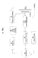
- FIG. 1 a block diagram is shown which illustrates a prior art capacitive displacement sensor 1.
- the "voltage drive to probe” 70 develops an A.C. voltage (excitation voltage) across the probe and target.
- the block 20 labeled “probe output-current sensor” represents the means by which the current through the probe is measured.
- the block 40 labeled " AC to DC converter” represents a circuit operative to change the A.C. probe output signal to a proportional D.C. value.
- Such circuits could include, but are not limited to, synchronous demodulators or diode rectification circuits.
- the block 50 labeled “comparator” compares the output of the AC to DC converter to a reference signal and provides an output indicative of the difference between the output of the AC to DC converter and the reference signal.
- the block 60 labeled “gain block” provides appropriate gain and phase characteristics for the loop formed by connecting the output of the gain block 60 to control the voltage-drive block 70.
- the loop functions to make the value at the output of the rectifier block 40 equal to the reference value 30.
- the probe's output current is held constant.
- the voltage across the probe is then measured. This measured voltage varies linearly with the spacing between the probe 10 and the target 15.
- the circuit of Fig. 1 by no means represents the only way to accomplish the goal of driving a capacitive probe at constant current. Additional gain blocks could be used or the gain could be applied at a different place in the loop; the output-current sensor and rectifier could be one in the same device; the rectifier could be eliminated and the whole circuit could work at the excitation frequency of the probe. Other differences are also possible.
- the open-loop gain of the capacitive displacement gauge is directly proportional to the probe capacitance, C p . Since the probe operates over some distance range the loop gain of the gauge will change as the probe-to-target distance changes. The distance ratio will produce a capacitance ratio of the same magnitude. The changing loop gain of the gauge causes an undesirable change in the frequency response of the loop, thus limiting the range of the capacitive displacement gauge.
- the circuitry of the capacitive displacement gauge can be slightly modified by the addition of a current mirror.
- a current mirror is designed to have an output current that is a fixed percentage of its input current.
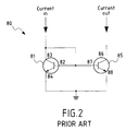
- a classic 1:1 current mirror circuit 80 is shown in Fig. 2.
- Two transistors 81 and 85 are shown and are configured such that the base 82 of the first transistor 81 is in electrical communication with the base 87 of second transistor 85.
- the base 82 of the first transistor 81 is also in electrical communication with the collector 83 of first transistor 81 and functions as the input to the current mirror 80.
- the emitter 84 of first transistor 81 and the emitter 88 of second transistor 85 are connected to ground.
- the collector 86 of second transistor 85 functions as the output of the current mirror 80. As long as the two transistors 81 and 85 are matched and thermally bonded, the output current will equal the input current.
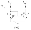
- a nonlinear current mirror is shown.
- the current mirror shown in Fig. 2 has been modified by the insertion of a resistor 90 between the emitter 84 of first transistor 81 and ground. This addition of the resistor into the current mirror causes a nonlinear response.
- the nonlinearity is directly related to the relationship between the current through an ideal transistor and its base-emitter voltage (v be ). Equation 8 shows the incremental relationship between v be and i c .
- V be1 - V be2 (Kk/q)ln(i c1/ i c2 )
- Equation 8 is modified to form Equation 9 wherein the voltage drop across the resistor 90 is included which is the v be that the output transistor sees.
- V be1 - V be2 (Kk/q)ln(i c1 /i c2 ) + r(i c1 - i c2 )
- Equation 9 the assumption has been made that the h fe of the transistors 81 and 85 is high enough to allow the collector currents and emitter currents to be considered equal. Equations 8 and 9 are combined to form the following equation which defines the relationship between the input and output currents of the nonlinear current mirror 100.
- the nonlinear current mirror 100 is placed between the output of the gain block 60 and the input to the voltage-drive block 70.
- the nonlinear current mirror could be placed in more than one place in the feedback loop. Because matched, monolithic transistors are readily and cheaply available, and because the component count is so low, the nonlinear current mirror circuit can be conveniently and cheaply built, requiring a minimum amount of board space.
- the feedback loop functions to keep i p constant, and the gain stages represented by the variable A are constant. Therefore, the loop gain is constant when di o /(di c i o ) is made constant.
Landscapes
- Physics & Mathematics (AREA)
- General Physics & Mathematics (AREA)
- Engineering & Computer Science (AREA)
- Power Engineering (AREA)
- Measurement Of Length, Angles, Or The Like Using Electric Or Magnetic Means (AREA)
- Length Measuring Devices With Unspecified Measuring Means (AREA)
- Control Of Electrical Variables (AREA)
- Amplifiers (AREA)
Applications Claiming Priority (2)
| Application Number | Priority Date | Filing Date | Title |
|---|---|---|---|
| US119803 | 1998-07-21 | ||
| US09/119,803 US6181142B1 (en) | 1998-07-21 | 1998-07-21 | Nonlinear current mirror for loop-gain control |
Publications (2)
| Publication Number | Publication Date |
|---|---|
| EP0974810A2 true EP0974810A2 (fr) | 2000-01-26 |
| EP0974810A3 EP0974810A3 (fr) | 2000-12-13 |
Family
ID=22386517
Family Applications (1)
| Application Number | Title | Priority Date | Filing Date |
|---|---|---|---|
| EP99401825A Withdrawn EP0974810A3 (fr) | 1998-07-21 | 1999-07-20 | Miroir de courant non-linéaire pour le réglage de gain de boucle |
Country Status (3)
| Country | Link |
|---|---|
| US (1) | US6181142B1 (fr) |
| EP (1) | EP0974810A3 (fr) |
| JP (1) | JP3522596B2 (fr) |
Cited By (2)
| Publication number | Priority date | Publication date | Assignee | Title |
|---|---|---|---|---|
| EP1944674A1 (fr) * | 2006-12-18 | 2008-07-16 | ATMEL Germany GmbH | Circuit destiné à la production d'une valeur de référence de tension ou de courant compensée par température |
| CN100412928C (zh) * | 2003-02-28 | 2008-08-20 | 精工爱普生株式会社 | 电流生成电路、电光学装置及电子机器 |
Families Citing this family (3)
| Publication number | Priority date | Publication date | Assignee | Title |
|---|---|---|---|---|
| US6457022B1 (en) * | 2000-06-05 | 2002-09-24 | International Business Machines Corporation | Methods, systems and computer program products for mirrored file access through forced permissions |
| JP6149953B1 (ja) | 2016-02-01 | 2017-06-21 | オンキヨー株式会社 | 保護回路、及び、スイッチング電源 |
| US11014194B2 (en) * | 2017-11-02 | 2021-05-25 | Coherent, Inc. | Laser material processing distance gauge |
Family Cites Families (19)
| Publication number | Priority date | Publication date | Assignee | Title |
|---|---|---|---|---|
| JPS5537958A (en) * | 1978-09-11 | 1980-03-17 | Hiromi Ogasawara | Rotation angle detector |
| US4234841A (en) * | 1979-02-05 | 1980-11-18 | Rca Corporation | Self-balancing bridge network |
| US4302718A (en) * | 1980-05-27 | 1981-11-24 | Rca Corporation | Reference potential generating circuits |
| US4521727A (en) * | 1983-05-23 | 1985-06-04 | Honeywell Inc. | Hall effect circuit with temperature compensation |
| GB8322002D0 (en) * | 1983-08-16 | 1983-09-21 | Atomic Energy Authority Uk | Gauging apparatus |
| US4649336A (en) * | 1985-01-29 | 1987-03-10 | Atomic Energy Of Canada Limited | Automatic, self sustaining probe for measuring the work function |
| JPS61283219A (ja) * | 1985-06-10 | 1986-12-13 | Omron Tateisi Electronics Co | 近接センサ発振回路 |
| US4814691A (en) * | 1985-08-09 | 1989-03-21 | Washington Research Foundation | Fringe field capacitive sensor for measuring profile of a surface |
| US5327030A (en) * | 1987-11-13 | 1994-07-05 | Analog Devices, Inc. | Decoder and monolithic integrated circuit incorporating same |
| US4843343A (en) * | 1988-01-04 | 1989-06-27 | Motorola, Inc. | Enhanced Q current mode active filter |
| US5070302A (en) * | 1989-09-05 | 1991-12-03 | Eastman Kodak Company | Capacitance probe for measuring a width of a clearance between parts |
| US5059916A (en) * | 1990-01-08 | 1991-10-22 | National Semiconductor Corporation | Gauge driver for use with a remote sensor and having reduced offset potential response |
| US5122755A (en) * | 1990-05-11 | 1992-06-16 | New Sd, Inc. | Capacitive position detector |
| US5432478A (en) * | 1994-01-21 | 1995-07-11 | Analog Devices, Inc. | Linear interpolation circuit |
| US5570060A (en) * | 1995-03-28 | 1996-10-29 | Sgs-Thomson Microelectronics, Inc. | Circuit for limiting the current in a power transistor |
| KR19990008200A (ko) * | 1996-02-28 | 1999-01-25 | 요트.게.아. 롤페즈 | 온도 보상이 가능한 기준 전압원 |
| US5708368A (en) * | 1996-03-07 | 1998-01-13 | Ade Corporation | Method and apparatus for emulation of a linear variable differential transducer by a capacitive gaging system |
| JP3719800B2 (ja) * | 1996-12-26 | 2005-11-24 | 沖電気工業株式会社 | 光通信装置および光通信システム |
| JP3119215B2 (ja) * | 1997-10-14 | 2000-12-18 | 日本電気株式会社 | 差動アンプ |
-
1998
- 1998-07-21 US US09/119,803 patent/US6181142B1/en not_active Expired - Fee Related
-
1999
- 1999-07-15 JP JP20194399A patent/JP3522596B2/ja not_active Expired - Fee Related
- 1999-07-20 EP EP99401825A patent/EP0974810A3/fr not_active Withdrawn
Cited By (2)
| Publication number | Priority date | Publication date | Assignee | Title |
|---|---|---|---|---|
| CN100412928C (zh) * | 2003-02-28 | 2008-08-20 | 精工爱普生株式会社 | 电流生成电路、电光学装置及电子机器 |
| EP1944674A1 (fr) * | 2006-12-18 | 2008-07-16 | ATMEL Germany GmbH | Circuit destiné à la production d'une valeur de référence de tension ou de courant compensée par température |
Also Published As
| Publication number | Publication date |
|---|---|
| JP2000136903A (ja) | 2000-05-16 |
| JP3522596B2 (ja) | 2004-04-26 |
| EP0974810A3 (fr) | 2000-12-13 |
| US6181142B1 (en) | 2001-01-30 |
Similar Documents
| Publication | Publication Date | Title |
|---|---|---|
| US4001718A (en) | Linear oscillator for proximity sensor | |
| US4667166A (en) | Differential amplifier system | |
| US6172555B1 (en) | Bandgap voltage reference circuit | |
| JPS6237440B1 (fr) | ||
| KR940005376B1 (ko) | 이득가변증폭기 | |
| JPH06188657A (ja) | 自動利得制御回路に指数関数段を接続する回路,自動利得制御回路及び温度補償回路 | |
| US4109214A (en) | Unbalanced-to-balanced signal converter circuit | |
| NL8401647A (nl) | Werkwijze en schakeling voor het compenseren van een temperatuurgevoelig element. | |
| US3435375A (en) | Controller having fet bridge circuit | |
| US5079454A (en) | Temperature compensated FET power detector | |
| US6181142B1 (en) | Nonlinear current mirror for loop-gain control | |
| US7015621B2 (en) | Piezoelectric actuator device | |
| JPH07141039A (ja) | 温度補償電圧発生回路 | |
| US3947706A (en) | Voltage and temperature compensated linear rectifier | |
| US4051446A (en) | Temperature compensating circuit for use with a crystal oscillator | |
| US5945873A (en) | Current mirror circuit with improved correction circuitry | |
| US4492932A (en) | Amplifier circuit having a high-impedance input and a low-impedance output | |
| US4719432A (en) | Oscillator for measuring temperature | |
| US20140062346A1 (en) | Switched capacitor charge pump driver for piezoelectric actuator | |
| JP2002185298A (ja) | 物理量検出回路 | |
| JPH0671190B2 (ja) | 集積可変容量性リアクタンス回路 | |
| JPH0528334B2 (fr) | ||
| EP0663584A1 (fr) | Dispositif de commande des vibrations pour la vibration d'un gyroscope | |
| JPH07111421A (ja) | ダイオード検波回路 | |
| US3466560A (en) | Stable amplifier having a stable quiescent point |
Legal Events
| Date | Code | Title | Description |
|---|---|---|---|
| PUAI | Public reference made under article 153(3) epc to a published international application that has entered the european phase |
Free format text: ORIGINAL CODE: 0009012 |
|
| AK | Designated contracting states |
Kind code of ref document: A2 Designated state(s): DE FR GB IT |
|
| AX | Request for extension of the european patent |
Free format text: AL;LT;LV;MK;RO;SI |
|
| RIC1 | Information provided on ipc code assigned before grant |
Free format text: 7G 01B 7/00 A, 7G 01D 5/00 B, 7G 05F 3/26 B |
|
| PUAL | Search report despatched |
Free format text: ORIGINAL CODE: 0009013 |
|
| AK | Designated contracting states |
Kind code of ref document: A3 Designated state(s): AT BE CH CY DE DK ES FI FR GB GR IE IT LI LU MC NL PT SE |
|
| AX | Request for extension of the european patent |
Free format text: AL;LT;LV;MK;RO;SI |
|
| 17P | Request for examination filed |
Effective date: 20010607 |
|
| AKX | Designation fees paid |
Free format text: DE FR GB IT |
|
| STAA | Information on the status of an ep patent application or granted ep patent |
Free format text: STATUS: THE APPLICATION HAS BEEN WITHDRAWN |
|
| 18W | Application withdrawn |
Effective date: 20050718 |